5
X
October 2017
32-Bit MIPS RISC Processor
K.Phanindra1. A.Sravanthi2, K.Vijayabharathi3
1
pg scholar, m.tech (es) kits, khammam 2
pg scholar, m.tech (dece) gnits, hyderabad, 3
pg scholar, m.tech (decs) spmvv, hyderabad,
Abstract: This paper concerned with the design and implementation of a 32 - bit Reduced Instruction Set Computer (RISC) processor on a Field Programmable Gate Arrays (FPGAs). The processor has been designed with VHDL, synthesized using Xilinx ISE 9.1i Webpack, simulated using ModelSim simulator, and then implemented on Xilinx Spartan 2E FPGA that has 143 available Input/Output pins and 50MHz clock oscillator. The results for the different parts of the processor are presented in the form of test bench wave form and the architecture of the system is demonstrated.
Keywords:FPGA, CPU, VHDL, RISC, Processor.
I. INTRODUCTION
Computer Engineering and Computer Design are very much concerned with the cost and performance of components in the implementation domain. Reduced Instruction Set Computer (RISC) focuses on reducing the number and complexity of instructions in the machine [1, 2]. Compared to ASIC design Field Programmable Gate Arrays (FPGAs) are growing fast with cost reduction [3]. The design of a low cost 32 - bit RISC Processor has been described using VHDL, and by using Xilinx FPGA some components have been implemented and tested [4, 5, 6, and 7]. Spartan2Edevelopmentboard,DIO1,and DIO2 extension boards from Digilent have been used for the hardware implementation. For synthesis and simulation the Web pack from Xilinx and ModelSim have been used. The text in this article is organized as follows; The introduction is given in section I; Section II is describe about MIPS processor; Section III is talking about the system architecture; The design of the Control Unit is given in section IV ; Insection V we define the main structure of the Data Path; The design of the ROM is given in section VI; Sections VII will presents the simulation results for the different parts of the processor; The conclusion and future work will be given at the end in section VIII.
II. THE MIPSPROCESSOR
The MIPS single-cycle processor plays out the errands of guideline bring, direction disentangle, execution, memory get to and compose back across the board clock cycle. To begin with the PC esteem is utilized as a deliver to list the guideline memory which supplies a 32-bit estimation of the following direction to beexecuted. This direction is then separated into the distinctive fields. The guidelines opcode field bits [31-26] are sent to a control unit to decide the kind of direction to execute. The sort of guideline then figures out which control signs are to be stated and what work the ALU is to perform, along these lines disentangling thedirection. The enroll record peruses in the asked for locations and yields the information values contained in these registers. These information qualities can then be worked on by the ALU whose operation is controlled by the control unit to either register a memory address (e.g. load or store), figure a math result (e.g. include, or potentially slt), or play out a think about (e.g. branch). In the event that the direction decoded is number juggling, the ALU result must be composed to an enlist. On the off chance that the guideline decoded is a heap or a store, the ALU result is then used to address the information memory. The last stride composes the ALU result or memory esteem back to the enroll record. The MIPS usage as with all processors comprises of two principle sorts of rationale components: combinational and successivecomponents.
III. SYSTEMARCHITECTURE
Figure.2 shows the three components of the RISC processor presented in this paper. The three components are the Control Unit (CU), the Data Path, and the ROM. The Central Processing Unit (CPU) has 17 instructions. The design of the processor will be describe in the followingsections.
Figure (2) SystemArchitecture Figure (3) State diagram of CUDesign
IV. DESIGN OF THE CONTROL UNIT
By using FSM (Finite State Machine) the control unit is designed and it allows each state to run at one clock cycle, the first state is the reset which initialize the CPU internal registers and variables. The machine goes to the reset state by enabling the reset signal for a certain number of clocks. The instruction fetching and decoding states are followed by the reset state. The instruction state is for reading instruction data from the ROM and the decoding state is decodes the parts of the instruction. Depending on the instruction the decoding state will also select the next state, since every instruction has its own set of states, based on the given instruction the control unit will jump to the correct state. After completion of all states of a running instruction, the last one will allow us to process the next instruction in the program so it returns to the fetch state. The state diagram of the control unit as shown in Figure.3.
V. DESIGN OF THE DATA PATH
Fig 4: Load word Data Path
The ALU design consists of two input ports and one output port which mainly performs operations on two operands. It has a design similar to the control unit based on a code given by the ALUCL it selects an operation. The Memory Interface was designedto accommodate simple load/store operations with the 16x32 memory. The effective address is calculated by adding the content of the address register and the immediate data. The Branch Unit calculates a given condition by the control unit and raises a branch flag whether the condition is met or not, and if the flag is raised, it sends the branch address back to the control unit in order to replace the program counter. The control lines coming from the control unit operate all the units in the data path. The path starts from the register file that has two output ports which are connected to all the other units, after that the processing is done by one of the other units then finally returned back to the register files input port using the multiplexer. The signals used in the data path are forwarded from the control unit to each subcomponent as needed.
Figure (5) the Sub-components of the Data Path
VI. DESIGN OF THE ROM
The CPU has a built in ROM which enables us to program simple code and execute it. It is a basic 16x32 ROM and it is 32bit aligned. The List of signals in the ROMis:
A. address: address sent by the controlunit
B. data_out: the data that is contained the given address
C. read: the signal to enable reading from the ROM
D. ready: the signal to indicate when the ROM is ready forreading
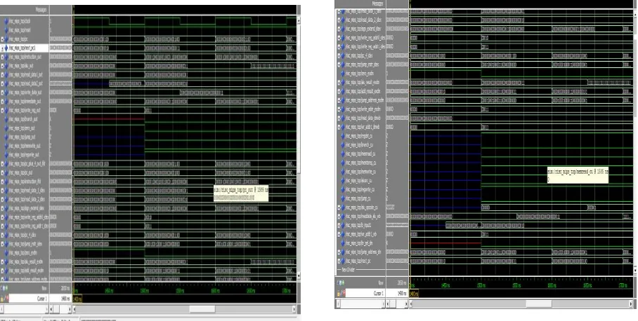
VII. SIMULATIONRESULTS Depictions of each snapshot of the application while running is given underneath:
Figure (6) Simulation results
VIII. CONCLUSION AND FUTUREWORK
32-bit RISC Process has been design and implemented in hardware on Xilinx Spartan 2E FPGA. The design has been achieved using VHDL and simulated with ModelSim. The hardware part has been used by the Digilent Spartan 2E development board. Most of the goals were achieved and simulation shows that the processor is working perfectly, but the Spartan 2E FPGA was not sufficient for implementing the whole design into a real hardware, since the total available logic gate in Spartan 2E is 200K Logic Gate, which was not enough for implementing the whole processor, but parts of the processor have been implemented and test in a real hardware. In future scope increasing the number of instructions and make a pipelined design with less clock cycles per instruction and more improvement can be added in the future work.
REFERENCES
[1] John L. Hennessy, and David A. Patterson, “Computer Architecture A Quantitative Approach”, 4th Edition; 2006.
[2] Vincent P. Heuring, and Harry F. Jordan, “Computer Systems Design and Architecture”, 2nd Edition,2003. [3] Wayne Wolf, FPGA - Based System Design, Prentice Hall,2005.
[4] Dal Poz, Marco Antonio Simon, Cobo, Jose EdinsonAedo, Van Noije, WilhelmusAdrianus Maria, Zuffo, Marcelo Knorich, “Simple Risc microprocessor core designed for digital set - top - box applications”, Proceedings of the International Conference on Application SpecificSystems, Architectures and Processors, 2000, p 35-44
[5] Brunelli Claudio, Cinelli Federico, Rossi Davide, NurmiJari, “A VHDL model and implementation of a coarse - grain reconfigurable coprocessor for a RISC core”, 2nd Conference on Ph.D. Research in MicroElectronics and Electronics - Proceedings, PRIME, 2006, p229-232
[6] Rainer Ohlendorf, Thomas Wild, Michael Meitinger, Holm Rauchfuss, Andreas Herkersdorf, “Simulated and measured performance evaluation of RISC - based SoC platforms in network processing applications”, Journal of Systems Architecture 53 (2007)703–718.
[7] Luker, Jarrod D., Prasad, Vinod B., “RISC system design in an FPGA”, MWSCAS 2001, v2, 2001,p532536
[8] Jiang, Hongtu; “FPGA implementation of controller - data path pair in custom image processor design”; IEEE International Symposium on Circuits and Systems - Proceedings; 2004, pV141V144
[9] K. Vlachos, T. Orphanoudakis, Y. Papaeftathiou, N. Nikolaou, D. Pnevmatikatos, G. Konstantoulakis, J.A. Sanchez - P., “Design and performance evaluation of a Programmable Packet Processing Engine (PPE) suitable for high - speed network processors units”, Microprocessors and Microsystems 31, 2007, p 188– 199
[10] Lou Dongjun, Yuan Jingkun, Li Daguang, Jacobs Chris, “Datapath verification with SystemC reference model”, ASICON 2005, 6th International Conference
[image:5.612.77.531.112.341.2]Mr.K.PHANINDRA has received his B.Tech in ECE from SwarnaBharathi Institute of Science & Technology, Khammam, affiliated to J.N.T.U Hyderabad in 2015. He is pursuing M.Tech in the stream of ES in Khammam Institute of Science & Technology, Khammam, T.S. His research interests include Embedded Systems, Image Processing & Digital Communication.
Ms.A.SRAVANTHI has received her B.Tech in ECE from SwarnaBharathi Institute of Science & Technology, Khammam, affiliated to J.N.T.U Hyderabad in 2015. She is pursuing M.Tech in the stream of DECE in G. Narayanamma Institute of Technology & Science, Hyderabad, T.S. Her research interests include Image Processing & Digital Communication.