Memory Design Using Logical Gates
Mandisha Sharma
1, Mansi Kakkar
2,ManishSharma
3 1, 2, 3B.Tech (Student)Department Of Computer Science, Dronacharya College Of Engineering, Gurgaon
Abstract: This research is about designing memory using logical gates. A memory unit is a collection of storage cells together with associated circuits needed to transform information in and out of the device. Memory cells which can be accessed for information transfer to or from any desired random location is called random access memory(RAM). The internal construction of a random-access memory of m words with n bits per word consists of m*n binary storage cells and associated decoding circuits for selecting individual words. A basic RAM cell has been provided here as a component which can be used to design larger memory units. An IC memory consisting of 4 words each having 3 bits has been also provided. In this research we will discuss about the designing of a RAM Cell and designing of 4*4 RAM.
Keywords:Flip-flops, Garbage Output, Random Access Memory, Reversible Logic, Quantum Cost. dynamic RAM array, reversible combinational circuits, reversible decoder.
I. INTRODUCTION
In recent year reversible computing has emerged as a promising technology. The primary reason for this is the increasing demands for low power devices. R. Landauer [1] proved that losing information causes loss of energy. Information is lost when an input cannot be recovered from its output. He showed that each bit of information loss generates kTln2 joules of heat
energy; where k is Boltzmann’s constant and T is the absolute
temperature at which computation is performed. C. H. Bennett [2] showed that energy dissipation problem can be avoided if circuits are built using reversible logic gates. One of the more interesting things that you can do with Boolean gates is to create memory with them. If you arrange the gates correctly, they will remember an input value. This simple concept is the basis of RAM (random access memory) in computers, and also makes it possible to create a wide variety of other useful circuits. Memory relies on a concept called feedback. That is, the output of a gate is fed back into the input.
Reversible logic is an emerging nanotechnology used in the design and implementation of nanotechnology and quantum computing with the main goal of reducing physical entropy gain. Significant work have been produced in the design of
recent developments in sequential design of reversible circuits has opened new avenues in the implementation of reversible combinational circuits, such as the design and implementation of random access memory. In this paper, a novel 4*4 MLMR gate is presented which is used for controlling the read/write logic of a SRAM cell. Next, a reversible SRAM cell is designed and verified. Then, a novel 4*4 Reversible Decoder (RD) gate, implemented as a 2-to-4 decoder with low delay and cost is presented and verified, and its implementation shown in the construction of a 4×2 reversible SRAM array. Next, a dual-port SRAM cell is presented and verified, and its implementation in a synchronous n-bit reversible dual-port SRAM array is shown. Then, a reversible DRAM cell is presented and verified. The control logic for writing to the DRAM based on Peres gates is shown. The control logic and the DRAM cell are then implemented in a reversible 4×4 DRAM array.
II. BASIC DEFINATIONS
In this section, some basic definitions related to reversible logic are presented. We formally define reversible gate, garbage output, delay and quantum cost in reversible circuits.
www.ijraset.com
Vol.2Issue IX, September2014
ISSN: 2321-9653
INTERNATIONAL JOURNAL FOR RESEARCH IN APPLIED SCIENCE AND
ENGINEERING TECHNOLOGY(IJRASET)
A Reversible Gate is a k-input, k-output (denoted by k*k) circuit that produces a unique output pattern for each possible input pattern [3]. Reversible Gates are circuits in which the number of outputs and inputs are equal and there is a one to one mapping between the vector of inputs and outputs. If the input vector is Iv
where Iv = (I1,j, I2,j, I3,j,…. , Ik-1,j, Ik,j) and the output vector
is Ov where Ov = (O1,j , O2,j , O3,j , … , Ok-1,j , Ok,j), then
according to the definition, for each particular vector j, Iv « Ov.
2.2 Garbage Output
Outputs that are not primary outputs or outputs that are not used as input to other gates to produce primary outputs are garbage. Unwanted or unused outputs which are needed to maintain reversibility of a reversible gate (or circuit) are known as Garbage Outputs. The garbage output of Feynman gate [7] is shown Figure 1 with *.
2.3 Delay
The delay of a logic circuit is the maximum number of gates in a path from any input line to any output line. The definition is based on two assumptions: (i) Every gate computation takes one unit of time and (ii) All inputs to the circuit are available before the computation. In this paper, we used the logical depth as measure of the delay proposed by Mohammadi and Eshghi [8]. The delay of each 1x1 gate and 2x2 reversible gate is taken as unit delay 1. Any 3x3 reversible gate can be designed from 1x1 reversible gates and 2x2 reversible gates, such as CNOT gate,
Controlled-V and Controlled-V+ gates (V is a square-root-of
NOT gate and V+ is its hermitian). Thus, the delay of a 3x3
reversible gate can be computed by calculating its logical depth when it is designed from smaller 1x1 and 2x2 reversible gates.
2.4 Quantum Cost
The quantum cost of a reversible gate is defined as the number of 1x1 and 2x2 reversible gates or quantum gates needed to realize the design. The quantum costs of all reversible 1x1 and 2x2 gates are taken as unity [9]. Since every reversible gate is a combination of 1x1 or 2x2 quantum gate, the quantum cost of any reversible gate can be calculated by counting the numbers of
NOT, Controlled-V, ControlledV+and CNOT gates used in the
design.
III. QUANTUM ANALYSIS OF POPULAR REVERSIBLE GATES
Every reversible gate can be realized by the quantum gates. Thus the cost of reversible circuit can be measured in terms of quantum cost. Reducing the quantum cost of a reversible circuit is always a challenging one and works are still going on in this area. This section describes some popular reversible gates and presents quantum equivalent diagram of each of the reversible gate.
3.1Reversible computation
• Landauer/Bennett: all operations required in computation
could be performed in a reversible manner, thus dissipating no heat!
• The first condition for any deterministic device to be reversible
is that its input and output be uniquely retrievable from each other - then it is called logically reversible.
• The second condition: a device can actually run backwards -then it is called physically reversible.
3.2Feynman Gate
The input vector, Ivand output vector, Ovfor 2*2 Feynman Gate
(FG) is defined as follows: Iv= (A, B) and Ov= (P = A, Q = A
B). The quantum cost of Feynman gate is 1. The block diagram and equivalent quantum representation for 2*2 Feynman gate are shown in Fig 1.
(b)
Figure 1. (a) Block diagram of 2x2 Feynman gate and (b) equivalent circuit
3.3Reversible fredkin gate
Reversible gate is a logical gate with one-to-one mapping i.e., for each input vector, there is a unique output vector and vice versa. Also known as reversible conservative logic.Fanout at the output is not allowed. The designs presented in this paper are based on conservative reversible (three inputs: three outputs) Fredkin gate shown it can be described as mapping (A,B, and C) to (P = A,Q = AB + AC, and R = AB + AC),where A,B, and C are the inputs, and P,Q, and R are the outputs, respectively. The operation involves: Whenever the first input (say A) is 1, the swapping of inputs B and C is done at the output. Otherwise, output is same as input. Table I shows the truth table of Fredkin Gate, and it can be seen thatFredkin gate produces the same
number of 1’s in the outputs as on the inputs, in addition to the
one-to-one mapping feature of reversibility.
– Fredkin Gate is a fundamental concept inreversible and
quantum computing.
–Every Boolean function can be buildfrom 3 * 3 Fredkin gates:
P = A,
Q = if A then C else B,
R = if A then B else C.
Figure 3. (a) Block diagram of 3*3 Frekdin gate and (b) Equivalent quantum s
3.4 Peres Gate
The input vector, Ivand output vector, Ovfor 3*3 Peres gate
(PG)[9] is defined as follows: Iv= (A, B, C) and Ov=
(P = A, Q = AB, R = ABC). The quantum cost of Peres gate
is 4. The block diagram and equivalent quantum representation for 3*3 Peres gate are shown in Figure 4.
Figure 4. (a) Block diagram of 3*3 Peres and (b) Equivalent
(a)
(b)
(a)
(b) (b)
Figure 1. (a) Block diagram of 2x2 Feynman gate and (b) equivalent circuit
3.3Reversible fredkin gate
Reversible gate is a logical gate with one-to-one mapping i.e., for each input vector, there is a unique output vector and vice versa. Also known as reversible conservative logic.Fanout at the output is not allowed. The designs presented in this paper are based on conservative reversible (three inputs: three outputs) Fredkin gate shown it can be described as mapping (A,B, and C) to (P = A,Q = AB + AC, and R = AB + AC),where A,B, and C are the inputs, and P,Q, and R are the outputs, respectively. The operation involves: Whenever the first input (say A) is 1, the swapping of inputs B and C is done at the output. Otherwise, output is same as input. Table I shows the truth table of Fredkin Gate, and it can be seen thatFredkin gate produces the same
number of 1’s in the outputs as on the inputs, in addition to the
one-to-one mapping feature of reversibility.
– Fredkin Gate is a fundamental concept inreversible and
quantum computing.
–Every Boolean function can be buildfrom 3 * 3 Fredkin gates:
P = A,
Q = if A then C else B,
R = if A then B else C.
Figure 3. (a) Block diagram of 3*3 Frekdin gate and (b) Equivalent quantum s
3.4 Peres Gate
The input vector, Ivand output vector, Ovfor 3*3 Peres gate
(PG)[9] is defined as follows: Iv= (A, B, C) and Ov=
(P = A, Q = AB, R = ABC). The quantum cost of Peres gate
is 4. The block diagram and equivalent quantum representation for 3*3 Peres gate are shown in Figure 4.
Figure 4. (a) Block diagram of 3*3 Peres and (b) Equivalent
(a)
(b)
(a)
[image:4.612.316.498.133.324.2] [image:4.612.319.534.483.626.2]www.ijraset.com
Vol.2Issue IX, September2014
ISSN: 2321-9653
INTERNATIONAL JOURNAL FOR RESEARCH IN APPLIED SCIENCE AND
ENGINEERING TECHNOLOGY(IJRASET)
4.PROPOSED MODIFICATION ON FREKDIN GATE
4.1Modified FRG 1 gate
The input vector, Ivand output vector, Ovfor 3*3 modified
4.2 Modified FRG 2 gate
The input vector Ivand output vector Ovof 3*3 modified
5. DESIGN OF RANDOM ACCESS MEMORY
In this section we first presented proposed design for all the components of RRAM. Then we presented our proposed novel design of RRAM that is optimized in terms of quantum cost, delay and garbage outputs.
5.1 Proposed Reversible n to 2nDecoder
A single Feynman gate can be used to design the basic 1 to 21
decoder. Using this decoder we can systematically add 2n-1
number of MRFG1 gates to the design to achieve n to 2n
decoder. The design of 1 to 21decoder is shown in Figure. 8.
Fig. 8. Proposed 1 to 21decoder
The design of decoder has 1 quantum cost, 1 delay and no garbage output.
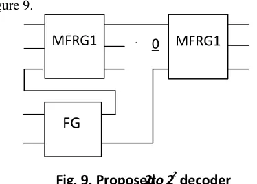
Our proposed 2 to 24decoder using MRFG1 gates are shown in
Figure 9.
The proposed 2 to 22decoder has quantum cost 9, delay 9 and
bare minimum of 1 garbage bit. The proposed design of 2 to 22
decoder achieves improvement ratios of 18%, 18% and 50% in terms of quantum cost, delay and garbage outputs compared to the design presented in N.M.Nayeem et al. [14]. The improvement ratios compared to the design M. Morrison et al. presented in [19] are 10% and 10% in terms of quantum cost
and delay. The comparison of proposed 2 to 22decoder with the
[image:5.612.324.511.287.421.2]existing ones shown in table I.
Table I. Comparison of different types of 2 to 22decoders.
2 to 22 decoder
design
Cost Comparisons Quantum
Cost
Delay Garbage Outputs
Proposed 9 9 1
Existing[14] 11 11 2
Existing[19] 10 10
-Improvement(%) 18 18 50
Fig. 9. Proposed
2
to
2
2decoder
0
̅
MFRG1
̅
̅ ̅
MFRG1
FG
Feynman
Gate
A
A
1
A
FredkinGate(MFRG 2)is defined as
I
v= (A
,
B
,
C)
and
O
v= (
AP
,
Q AB AC,
R AC AB). The quantum cost of
MFRG2 gate is 5.
Fig. 7. Quantum representation of MFRG gate
2
V
V
V
+A
C
B
Q ABACAB C A R
A P
Fredkin Gate (MFRG is defined as follows:
1)
I
v= (A
,
B
,
C)
and
O
v=(
P=A,
Q AB AC,
R AC AB).
The
quantum
cost of MFRG1 gate is 4.
Fig. 6. Quantum representation of MFRG 1gate
V
V
V
+A
B
C
C A B A
Q
P = A
[image:5.612.306.490.564.664.2]w.r.t. [14] Improvement(%) w.r.t. [19]
10 10
-Theorem 1: To construct n to 2 n decoder, if g is the total
number of gates required to design the decoder producing b
number of garbage outputs then g≥ 2n-1 and b≥ n-1.
Proof: For 1 to 21decoder only one Feynman gate needed that
doesn’t produce any garbage bit. So number of gate = 1 and
garbage output = 0.
Now for n>1, n to 2ndecoder design requires that each of the
output of the (n-1) to 2(n-1)decoders together with (n-1) selection
bits are employed in separate MRFG1 gate to produce selections
for n to 2ndecoder. In that case overall number of gates becomes
2n-1, because for n=1 we were required only 1 gate. This design
has n-1 garbage bits as the 1 to 21 decoder produces zero
garbage.
Theorem 2: The quantum cost of an n to 2ndecoder is Qc≥ 4.2n
-7.
Proof: From theorem 1, at least 2n-1 gates are required to design
n to 2n decoder. For n = 1 only one 2*2 Feynman gate is
required which has quantum cost 1. Then 2n-2 MRFG1 gates are
required and each MRF1 gate’s quantum cost is 4. So total
quantum cost Qcis = (2n-2)4 +1 = 4.2n-7.
5.2 Proposed Single bit Memory Cell
The heart of our proposed memory block is D flip-flop. The
characteristic equation of gated D flip-flop is Q+=
.D+ .Q. The D flip-flop can be realized by one MFRG2
gate and one FG. It can be mapped with MFRG2 by giving CLK
, D and Q respectively in 1st, 2ndand 3rdinputs of MFRG2 gate.
The Figure 10 shows our proposed D flip-flop with and ̅
[image:6.612.364.492.135.231.2]outputs.
Fig. 10: Proposed design of D flip-flop with and ̅outputs.
The proposed D flip-flop with and ̅outputs has quantum cost
7, delay 7 and has the bare minimum of 1 garbage bit. The proposed design of gated D flip-flop achieves improvement ratios of 50% in terms of garbage outputs compared to the design presented in Thapliyal et al. 2010[15] and L. Jamal et al.
2012[16]. The comparisons of our D flipflop (with and ̅
outputs) design with existing designs in literature are summarized in Table II.
Table II. Comparison of different types of D flip-flops with
and ̅outputs.
D flip-flop design
Cost Comparisons Quantum
Cost
Delay Garbage Outputs
Proposed 7 7 1
Existing[15] 7 7 2
Existing[16] 7 7 2
Improvement(%) w.r.t.
[15]
0 0 50
Improvement(%) w.r.t.
[16]
0 0 50
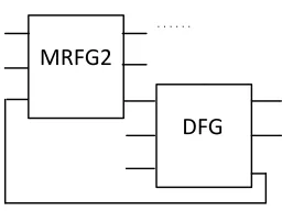
We need Write Enable Master Slave D FFs to design a Reversible Random Access Memory (RRAM). Our proposed write enable master slave flip-flop is shown in Figure 11.
̅
̅ ̅ ̅ ̅ ̅ ̅
DFG
MRFG2
w.r.t. [14] Improvement(%) w.r.t. [19]10 10
-Theorem 1: To construct n to 2 n decoder, if g is the total
number of gates required to design the decoder producing b
number of garbage outputs then g≥ 2 n-1 and b≥ n-1.
Proof: For 1 to 21decoder only one Feynman gate needed that
doesn’t produce any garbage bit. So number of gate = 1 and
garbage output = 0.
Now for n>1, n to 2ndecoder design requires that each of the
output of the (n-1) to 2(n-1)decoders together with (n-1) selection
bits are employed in separate MRFG1 gate to produce selections
for n to 2ndecoder. In that case overall number of gates becomes
2n-1, because for n=1 we were required only 1 gate. This design
has n-1 garbage bits as the 1 to 21 decoder produces zero
garbage.
Theorem 2: The quantum cost of an n to 2ndecoder is Qc≥ 4.2n
-7.
Proof: From theorem 1, at least 2n-1 gates are required to design
n to 2n decoder. For n = 1 only one 2*2 Feynman gate is
required which has quantum cost 1. Then 2n-2 MRFG1 gates are
required and each MRF1 gate’s quantum cost is 4. So total
quantum cost Qcis = (2n-2)4 +1 = 4.2n-7.
5.2 Proposed Single bit Memory Cell
The heart of our proposed memory block is D flip-flop. The
characteristic equation of gated D flip-flop is Q+=
.D+ .Q. The D flip-flop can be realized by one MFRG2
gate and one FG. It can be mapped with MFRG2 by giving CLK
, D and Q respectively in 1st, 2ndand 3rdinputs of MFRG2 gate.
The Figure 10 shows our proposed D flip-flop with and ̅
[image:6.612.307.549.390.535.2]outputs.
Fig. 10: Proposed design of D flip-flop with and ̅outputs.
The proposed D flip-flop with and ̅outputs has quantum cost
7, delay 7 and has the bare minimum of 1 garbage bit. The proposed design of gated D flip-flop achieves improvement ratios of 50% in terms of garbage outputs compared to the design presented in Thapliyal et al. 2010[15] and L. Jamal et al.
2012[16]. The comparisons of our D flipflop (with and ̅
outputs) design with existing designs in literature are summarized in Table II.
Table II. Comparison of different types of D flip-flops with
and ̅outputs.
D flip-flop design
Cost Comparisons Quantum
Cost
Delay Garbage Outputs
Proposed 7 7 1
Existing[15] 7 7 2
Existing[16] 7 7 2
Improvement(%) w.r.t.
[15]
0 0 50
Improvement(%) w.r.t.
[16]
0 0 50
We need Write Enable Master Slave D FFs to design a Reversible Random Access Memory (RRAM). Our proposed write enable master slave flip-flop is shown in Figure 11.
̅
̅ ̅ ̅ ̅ ̅ ̅
DFG
MRFG2
w.r.t. [14] Improvement(%) w.r.t. [19]10 10
-Theorem 1: To construct n to 2 n decoder, if g is the total
number of gates required to design the decoder producing b
number of garbage outputs then g≥ 2n-1 and b≥ n-1.
Proof: For 1 to 21decoder only one Feynman gate needed that
doesn’t produce any garbage bit. So number of gate = 1 and
garbage output = 0.
Now for n>1, n to 2ndecoder design requires that each of the
output of the (n-1) to 2(n-1)decoders together with (n-1) selection
bits are employed in separate MRFG1 gate to produce selections
for n to 2ndecoder. In that case overall number of gates becomes
2n-1, because for n=1 we were required only 1 gate. This design
has n-1 garbage bits as the 1 to 21 decoder produces zero
garbage.
Theorem 2: The quantum cost of an n to 2ndecoder is Qc≥ 4.2n
-7.
Proof: From theorem 1, at least 2n-1 gates are required to design
n to 2n decoder. For n = 1 only one 2*2 Feynman gate is
required which has quantum cost 1. Then 2n-2 MRFG1 gates are
required and each MRF1 gate’s quantum cost is 4. So total
quantum cost Qcis = (2n-2)4 +1 = 4.2n-7.
5.2 Proposed Single bit Memory Cell
The heart of our proposed memory block is D flip-flop. The
characteristic equation of gated D flip-flop is Q+=
.D+ .Q. The D flip-flop can be realized by one MFRG2
gate and one FG. It can be mapped with MFRG2 by giving CLK
, D and Q respectively in 1st, 2ndand 3rdinputs of MFRG2 gate.
The Figure 10 shows our proposed D flip-flop with and ̅
outputs.
Fig. 10: Proposed design of D flip-flop with and ̅outputs.
The proposed D flip-flop with and ̅outputs has quantum cost
7, delay 7 and has the bare minimum of 1 garbage bit. The proposed design of gated D flip-flop achieves improvement ratios of 50% in terms of garbage outputs compared to the design presented in Thapliyal et al. 2010[15] and L. Jamal et al.
2012[16]. The comparisons of our D flipflop (with and ̅
outputs) design with existing designs in literature are summarized in Table II.
Table II. Comparison of different types of D flip-flops with
and ̅outputs.
D flip-flop design
Cost Comparisons Quantum
Cost
Delay Garbage Outputs
Proposed 7 7 1
Existing[15] 7 7 2
Existing[16] 7 7 2
Improvement(%) w.r.t.
[15]
0 0 50
Improvement(%) w.r.t.
[16]
0 0 50
We need Write Enable Master Slave D FFs to design a Reversible Random Access Memory (RRAM). Our proposed write enable master slave flip-flop is shown in Figure 11.
̅
̅ ̅ ̅ ̅ ̅ ̅
www.ijraset.com
Vol.2Issue IX, September2014
ISSN: 2321-9653
INTERNATIONAL JOURNAL FOR RESEARCH IN APPLIED SCIENCE AND
ENGINEERING TECHNOLOGY(IJRASET)
As data are both read from and written into RAM, each FlipFlop should work on two modes- read and write. A MFRG1 gate is
used to multiplex between flip-flop’sD input and stored bit Q in
the flip-flop. When ‘write’ is high, input D of the MRFG1 gate
is carried to the first D flip-flop and if ‘write’ is low, output of
the D flip-flop is fed back to the second input of the MRFG1 gate so that state of the flip-flop remains same.
The proposed write enable master slave D flip-flop has quantum cost 17, delay 17 and 3 garbage bits. The proposed design of single bit memory cell achieves improvement ratios of 19% and 11% in terms of quantum cost and delay compared to the design
presented in M. Morrison [19]. The comparisons are summarized in table III.
Table III. Comparisons of different types of Write Enable
Master Slave D flip-flops with and ̅outputs.
Single bit Memory Cell
Cost Comparisons Quantum
Cost
Delay Garbage
Outputs
Proposed 17 17 3
Existing[19] 21 19
-Improvement in (%) 19 11
-5.3 Proposed Reversible Random Access Memory (RRAM)
A RAM is a two dimensional array of flip-flops. There are 2
nrows where each row contains m flip-flops. Each time only one
of the 2noutput lines of the decoder is active which selects one
row of flip-flops of the RAM. Whether a read or a write operation is performed depends on the W input. When W is high,
m flip-flops of the selected row of the RAM are written with the
inputs D1to Dm. When W is low, Q1to Qmcontains stored bits in
the flops of the selected row and simultaneously the flip-flops are refreshed with the stored bits. The proposed design of
2n*m bit RRAM is shown in Figure.12.
Theorem 3
Let g be the number of gates required to realize a 2n*
mReversible RAM where n be the number of bits and m be
the selection bits in the RRAM, then g ≥2n *(6m+2)
+m-1.Proof: A 2n * m RRAM requires n to2ndecoder that
consists of (2n-1) gates. 2nToffoli gates are required to
perform AND operations in RRAM. m*2nD flip-flops are
required inside the m * 2nRRAM whereas each D flip-flop
requires 5 gates. 2n * m Feynman gates are required to
perform the copy operation. There are m number of 2n bit
Feynman gate at the blottom last row. If g be the minimum
number of gates to realize the RRAM, then g≥(2n-1) + 2n+
5*2n*m + 2n*m+m Hence g≥ 2n*(6m+2)+m -1.
Theorem 4
Let n be the number of bits, m be the selection bits in the RRAM and bbe the number of garbage outputs generated
from the RRAM, then b≥ m*(4.2n-1)+n.
Proof: A 2n * m RRAM requires n to2ndecoder which
produces (n-1) garbage bits. 1 garbage bit is generated from
the mthToffoli gate in the RRAM. Inside RRAM there are
2n*m D flip-flops and each D flip-flop produces 3 garbage
bits. The last row contains m number of 2nbit Feynman gate
and each of them produces 2n-1garbage bits. If b be the
number of
garba *m + m*(2 -1).Hence b≥ m*(4.2n-1) + n.
Fig. 11: Proposed write enable master slave D flip
-flop.
g
20
FG
CLK
MFRG1
W
D
Q
W
̅ ̅ ̅ ̅ ̅ ̅
D FG
Q
MFRG2
CLK
g
1g
3MFRG2
www.ijraset.com
Vol.2Issue IX, September2014
ISSN: 2321-9653
INTERNATIONAL JOURNAL FOR RESEARCH IN APPLIED SCIENCE AND
ENGINEERING TECHNOLOGY(IJRASET)
As data are both read from and written into RAM, each FlipFlop should work on two modes- read and write. A MFRG1 gate is
used to multiplex between flip-flop’sD input and stored bit Q in
the flip-flop. When ‘write’ is high, inputD of the MRFG1 gate
is carried to the first D flip-flop and if ‘write’ is low, output of
the D flip-flop is fed back to the second input of the MRFG1 gate so that state of the flip-flop remains same.
The proposed write enable master slave D flip-flop has quantum cost 17, delay 17 and 3 garbage bits. The proposed design of single bit memory cell achieves improvement ratios of 19% and 11% in terms of quantum cost and delay compared to the design
presented in M. Morrison [19]. The comparisons are summarized in table III.
Table III. Comparisons of different types of Write Enable
Master Slave D flip-flops with and ̅outputs.
Single bit Memory Cell
Cost Comparisons Quantum
Cost
Delay Garbage
Outputs
Proposed 17 17 3
Existing[19] 21 19
-Improvement in (%) 19 11
-5.3 Proposed Reversible Random Access Memory (RRAM)
A RAM is a two dimensional array of flip-flops. There are 2
nrows where each row contains m flip-flops. Each time only one
of the 2noutput lines of the decoder is active which selects one
row of flip-flops of the RAM. Whether a read or a write operation is performed depends on the W input. When W is high,
m flip-flops of the selected row of the RAM are written with the
inputs D1to Dm. When W is low, Q1to Qmcontains stored bits in
the flops of the selected row and simultaneously the flip-flops are refreshed with the stored bits. The proposed design of
2n*m bit RRAM is shown in Figure.12.
Theorem 3
Let g be the number of gates required to realize a 2n*
mReversible RAM where n be the number of bits and m be
the selection bits in the RRAM, then g ≥2n *(6m+2)
+m-1.Proof: A 2n * m RRAM requires n to2ndecoder that
consists of (2n-1) gates. 2nToffoli gates are required to
perform AND operations in RRAM. m*2nD flip-flops are
required inside the m * 2nRRAM whereas each D flip-flop
requires 5 gates. 2n * m Feynman gates are required to
perform the copy operation. There are m number of 2n bit
Feynman gate at the blottom last row. If g be the minimum
number of gates to realize the RRAM, then g≥(2n-1) + 2n+
5*2n*m + 2n*m+m Hence g≥ 2n*(6m+2)+m -1.
Theorem 4
Let n be the number of bits, m be the selection bits in the RRAM and bbe the number of garbage outputs generated
from the RRAM, then b≥ m*(4.2n-1)+n.
Proof: A 2n * m RRAM requires n to2ndecoder which
produces (n-1) garbage bits. 1 garbage bit is generated from
the mthToffoli gate in the RRAM. Inside RRAM there are
2n*m D flip-flops and each D flip-flop produces 3 garbage
bits. The last row contains m number of 2nbit Feynman gate
and each of them produces 2n-1garbage bits. If b be the
number of
garba *m + m*(2 -1).Hence b≥ m*(4.2n-1) + n.
Fig. 11: Proposed write enable master slave D flip
-flop.
g
20
FG
CLK
MFRG1
W
D
Q
W
̅ ̅ ̅ ̅ ̅ ̅
D FG
Q
MFRG2
CLK
g
1g
3MFRG2
www.ijraset.com
Vol.2Issue IX, September2014
ISSN: 2321-9653
INTERNATIONAL JOURNAL FOR RESEARCH IN APPLIED SCIENCE AND
ENGINEERING TECHNOLOGY(IJRASET)
As data are both read from and written into RAM, each FlipFlop should work on two modes- read and write. A MFRG1 gate is
used to multiplex between flip-flop’sD input and stored bit Q in
the flip-flop. When ‘write’ is high, input D of the MRFG1 gate
is carried to the first D flip-flop and if ‘write’ is low, output of
the D flip-flop is fed back to the second input of the MRFG1 gate so that state of the flip-flop remains same.
The proposed write enable master slave D flip-flop has quantum cost 17, delay 17 and 3 garbage bits. The proposed design of single bit memory cell achieves improvement ratios of 19% and 11% in terms of quantum cost and delay compared to the design
presented in M. Morrison [19]. The comparisons are summarized in table III.
Table III. Comparisons of different types of Write Enable
Master Slave D flip-flops with and ̅outputs.
Single bit Memory Cell
Cost Comparisons Quantum
Cost
Delay Garbage
Outputs
Proposed 17 17 3
Existing[19] 21 19
-Improvement in (%) 19 11
-5.3 Proposed Reversible Random Access Memory (RRAM)
A RAM is a two dimensional array of flip-flops. There are 2
nrows where each row contains m flip-flops. Each time only one
of the 2noutput lines of the decoder is active which selects one
row of flip-flops of the RAM. Whether a read or a write operation is performed depends on the W input. When W is high,
m flip-flops of the selected row of the RAM are written with the
inputs D1to Dm. When W is low, Q1to Qmcontains stored bits in
the flops of the selected row and simultaneously the flip-flops are refreshed with the stored bits. The proposed design of
2n*m bit RRAM is shown in Figure.12.
Theorem 3
Let g be the number of gates required to realize a 2n*
mReversible RAM where n be the number of bits and m be
the selection bits in the RRAM, then g ≥2n *(6m+2)
+m-1.Proof: A 2n * m RRAM requires n to2ndecoder that
consists of (2n-1) gates. 2nToffoli gates are required to
perform AND operations in RRAM. m*2nD flip-flops are
required inside the m * 2nRRAM whereas each D flip-flop
requires 5 gates. 2n * m Feynman gates are required to
perform the copy operation. There are m number of 2n bit
Feynman gate at the blottom last row. If g be the minimum
number of gates to realize the RRAM, then g≥(2n-1) + 2n+
5*2n*m + 2n*m+m Hence g≥ 2n*(6m+2)+m -1.
Theorem 4
Let n be the number of bits, m be the selection bits in the RRAM and bbe the number of garbage outputs generated
from the RRAM, then b≥ m*(4.2n-1)+n.
Proof: A 2n * m RRAM requires n to2ndecoder which
produces (n-1) garbage bits. 1 garbage bit is generated from
the mthToffoli gate in the RRAM. Inside RRAM there are
2n*m D flip-flops and each D flip-flop produces 3 garbage
bits. The last row contains m number of 2nbit Feynman gate
and each of them produces 2n-1garbage bits. If b be the
number of
garba *m + m*(2 -1).Hence b≥ m*(4.2n-1) + n.
Fig. 11: Proposed write enable master slave D flip
-flop.
g
20
FG
CLK
MFRG1
W
D
Q
W
̅ ̅ ̅ ̅ ̅ ̅
D FG
Q
MFRG2
CLK
g
1g
3 [image:7.612.49.333.113.319.2]Fig.12. Proposed design of 2n* m bit RRAM
Theorem 5
Let n be the number of bits, mbe the selection bits in the
RRAM and Qcbe the quantum cost of the RRAM, then Qc≥
2n(19m+9)-7.
Proof: A 2n* m RRAM requires an n to2ndecoders that has
quantum cost 4.2n-7. 2nToffoli gates are used to perform
AND operations in RRAM where each of the gates has
quantum cost 5, m*2n DFFs are required inside the m *
2nRRAM whereas each DFF has quantum cost 17. 2n * m
Feynman gates are required to perform the copy operation where each of them has quatum cost 1. There are m number
of 2nbit Feynman gate in last row where each of them has
quantum cost 2n. If Qc be the quantum cost of RRAM then
Qc≥ 4.2n-7 +5.2n+ m*2n+17*m*2n+ m*2n.
Hence Qc≥ 2n(19m+9)-7
6. CONCLUSION
Reversible Random Access Memory (RRAM) is going to take the place of existing main memory in the forthcoming quantum devices. In this paper we proposed optimized RRAM with the help of proposed MRFG1 and MRFG2 gates along with some basic reversible logic gates. Appropriate algorithms and theorems are presented here to clarify the
our design with existing ones in literature which claims our success in terms of quantum cost, number of garbage outputs and delay. We believe this optimization can contribute significantly in reversible logic community.
7. ACKNOWLEDGMENTS
The authors would like to thank the anonymous referees for their constructive feedback, which helped significantly improving technical quality of this paper.
8. REFERNCES
[1] Rolf Landauer, "Irreversibility and Heat Generation in
the Computing Process", IBM Journal of Research and
Development, vol. 5, pp. 183-191, 1961.
[2] Charles H.Bennett, "Logical Reversibility of
computation", IBM Journal of Research and
Development, vol. 17, no. 6, pp. 525-532, 1973.
[3] Perkowski, M., A.Al-Rabadi, P. Kerntopf, A. Buller, M.
Chrzanowska-Jeske, A. Mishchenko, M. Azad Khan, A. Coppola, S. Yanushkevich, V. Shmerko and L.
Jozwiak, “A general decomposition for reversible logic”, Proc. RM’2001, Starkville, pp: 119-138, 2001
[4] J.E Rice, "A New Look at Reversible Memory
Elements", Proceedings International Symposium on
Circuits and Systems(ISCAS) 2006, Kos, Greece, May
21-24 ,2006, pp. 243-246.
[5] Dmitri Maslov and D. Michael Miller, “Comparison of
the cost metrics for reversible and quantum logic
synthesis”, http://arxiv.org/abs/quant-ph/0511008, 2006
[6] Hafiz Md.HasanBabu, Md.Rafiqul Islam, Ahsan Raja
Chowdhury, and Syed Mostahed Ali Chowdhury, "Synthesis of full-adder circuit using reversible logic,"
International Conference on VLSI Design, vol. 17, pp.
757-760, 2004.
[7] Richard P.Feynman, "Quantum mechanical computers,"
Foundations of Physics, vol. 16, no. 6, pp. 507-531,
1986.
[8] Mohammadi,M. and Mshghi,M, On figures ofmerit in
reversible and quantumlogic designs, Quantum Inform.
Process. 8, 4, 297–318, 2009.
Fig.12. Proposed design of 2n* m bit RRAM
Theorem 5
Let n be the number of bits, mbe the selection bits in the
RRAM and Qcbe the quantum cost of the RRAM, then Qc≥
2n(19m+9)-7.
Proof: A 2n* m RRAM requires an n to2ndecoders that has
quantum cost 4.2n-7. 2nToffoli gates are used to perform
AND operations in RRAM where each of the gates has
quantum cost 5, m*2n DFFs are required inside the m *
2nRRAM whereas each DFF has quantum cost 17. 2n * m
Feynman gates are required to perform the copy operation where each of them has quatum cost 1. There are m number
of 2n bit Feynman gate in last row where each of them has
quantum cost 2n. If Qc be the quantum cost of RRAM then
Qc≥ 4.2n-7 +5.2n+ m*2n+17*m*2n+ m*2n.
Hence Qc≥ 2n(19m+9)-7
6. CONCLUSION
Reversible Random Access Memory (RRAM) is going to take the place of existing main memory in the forthcoming quantum devices. In this paper we proposed optimized RRAM with the help of proposed MRFG1 and MRFG2 gates along with some basic reversible logic gates. Appropriate algorithms and theorems are presented here to clarify the
our design with existing ones in literature which claims our success in terms of quantum cost, number of garbage outputs and delay. We believe this optimization can contribute significantly in reversible logic community.
7. ACKNOWLEDGMENTS
The authors would like to thank the anonymous referees for their constructive feedback, which helped significantly improving technical quality of this paper.
8. REFERNCES
[1] Rolf Landauer, "Irreversibility and Heat Generation in
the Computing Process", IBM Journal of Research and
Development, vol. 5, pp. 183-191, 1961.
[2] Charles H.Bennett, "Logical Reversibility of
computation", IBM Journal of Research and
Development, vol. 17, no. 6, pp. 525-532, 1973.
[3] Perkowski, M., A.Al-Rabadi, P. Kerntopf, A. Buller, M.
Chrzanowska-Jeske, A. Mishchenko, M. Azad Khan, A. Coppola, S. Yanushkevich, V. Shmerko and L.
Jozwiak, “A general decomposition for reversible logic”, Proc. RM’2001, Starkville, pp: 119-138, 2001
[4] J.E Rice, "A New Look at Reversible Memory
Elements", Proceedings International Symposium on
Circuits and Systems(ISCAS) 2006, Kos, Greece, May
21-24 ,2006, pp. 243-246.
[5] Dmitri Maslov and D. Michael Miller, “Comparison of
the cost metrics for reversible and quantum logic
synthesis”, http://arxiv.org/abs/quant-ph/0511008, 2006
[6] Hafiz Md.HasanBabu, Md.Rafiqul Islam, Ahsan Raja
Chowdhury, and Syed Mostahed Ali Chowdhury, "Synthesis of full-adder circuit using reversible logic,"
International Conference on VLSI Design, vol. 17, pp.
757-760, 2004.
[7] Richard P.Feynman, "Quantum mechanical computers,"
Foundations of Physics, vol. 16, no. 6, pp. 507-531,
1986.
[8] Mohammadi,M. and Mshghi,M, On figures ofmerit in
reversible and quantumlogic designs, Quantum Inform.