ISSN: 1992-8645 www.jatit.org E-ISSN: 1817-3195
LOW POWER AND AREA- EFFICIENT HALF ADDER
BASED CARRY SELECT ADDER DESIGN USING COMMON
BOOLEAN LOGIC FOR PROCESSING ELEMENT
1R DHANABAL, 2DEEPIKA SRIVASTAVA, 3BHARATHI V
1Assistant Professor (Senior Grade), VLSI division, SENSE, VIT University, Vellore, TN, INDIA 2Student, VLSI division, SENSE, VIT University Vellore, TN, INDIA
3
Assistant Professor, GGR College of Engineering, Anna University, Vellore, TN, INDIA E-mail: [email protected], [email protected]
,
[email protected]ABSTRACT
Carry select adder is the one among the fastest adder used in the data processing element however conventional carry select adder(CSLA) are still area-consuming due to multiple pair of Ripple carry adder structure. This proposed work is solely dedicated to develop a low power and area efficient half adder based carry select adder architecture (CSLA) using common Boolean logic (CBL). It only needs one Half-adder to perform summation operation for carry zero and common Boolean logic (CBL) for carry one respectively. Half adder has been designed using one XOR gate and one AND gate. CBL needs only one OR gate and one NOT gate. Through the multiplexer, we can select the correct output in the final stage according to the logic state of the carry-in- signal. Based on this modification 8-bit, 16-bit, 32-bit, 64-bit square root carry select adder (SQRT CSLA) architecture has been developed and compared with the regular SQRT CSLA structure and modified SQRT CSLA has been developed using binary to excess-1 converter (BEC). This proposed design on an average reduces area by 53.77%, power consumption by 93% and power-delay product (PDP) by 75.71%, but with some amount of increase in the delay as compared with regular SQRT CSLA architecture. The result analysis shows that the proposed CSLA architecture achieves better performance in term of area, power and power-delay product than the regular and modified SQRT CSLA structure.
Keywords:ASIC, CSLA, RCA, BEC, Boolean-logic, Area-efficient, Low power.
1. INTRODUCTION
Addition is the most fundamental arithmetic operation widely impacts the overall performance of processing elements. In digital adders, the speed of addition is limited by the time required to propagate a carry sequentially only after the previous bit position has been summed and a carry propagated into the next position.
The CSLA is used in many arithmetic systems to eliminate the problem of carry propagation delay by using multiple pair of RCA blocks which helps in generating the partial sum for with and without carry therefore conventional CSLA is not area efficient. The final required sum and carry are selected by the multiplexers (mux).
The existing modified SQRT CSLA has used the Binary to excess-1 converter (BEC) in place of RCA for cin=1 in the regular CSLA to achieve lower area and power consumption with slightly increase in the delay.
The basic idea of proposed architecture to generate one bit partial sum and carry for cin=0 using Half adder and common Boolean logic (CBL) to replace the BEC in order to achieve best performance in term of area and power. Common Boolean logic requires only one OR gate and one NOT gate. The required sum is selected using multiplexer according to the logic state of the input signal of the multiplexer.
This paper is structured as follows. Section II and section III explain the regular and modified SQRT CSLA and detail structure of BEC respectively. Section IV and Section V deal with basic concept of Half Adder based CSLA using Common Boolean Logic (CBL) and proposed architecture respectively. Comparison of adders in terms of area, power and delay, results are analyzed in the section VI. Finally, this work has been concluded in Section VII.
2.REGULAR SQRT CSLA STRUCTURE:
The basic structure of regular square root carry select adder comprises of multiple pair of uniform block of ripple carry adders with multiplexer, the main drawback is that it has the large area and delay. The regular 16-bit carry select adder is shown in Fig.1. It is divided into many stages of non-uniform blocks of ripple carry adder (RCA) to generate the partial sum for cin=0 and cin=1. The carry out is calculated from the last stage. The selection of required sum done by using multiplexer. The advantage of regular SQRT CSLA with non-uniform RCA block is that it requires less area and increases the speed of operation. In fig.1 the 16-bit SQRT CSLA divided into five groups with different bit size RCA. Internal structure of the group 3 of regular 16-bit CSLA is shown fig.2. By manually counting the number of gates used for group 3 is 87 (full adder, half adder, and multiplexer).[1] One input to the multiplexer goes from the RCA with cin=0 and other input from the RCA with cin=1. In every stage the size of the multiplexer will also vary due to the change in the no. of inputs and outputs.
Cin
SUM[1:0] 2
2 2
[1:0]RCA 0
1 0
1 0
1 0
1 [15:11]RCA
[15:11]RCA
10 2
CY MUX
12:6
CoutSUM[15:11] 5
[10:7]RCA
[10:7]RCA
8 2
CY MUX
10:5
4
SUM[10:7]
[6:4]RCA
[6:4]RCA
6 2
CY MUX 8:4
3
SUM[6:4]
[3:2]RCA
[3:2]RCA
4 2
CY MUX
6:3
SUM[3:2] 2 2 3 3 4 4 5 5
B[15:11]
A[15:11] A[10:7] B[10:7] A[6:4] B[6:4] B[3:2]
A[3:2] A[1:0]B[1:0]
2 C1[7] C3[10]
C6[13] C10[16]
Fig.1 Regular 16-Bit SQRT CSLA
F F F
5 6
7
b a a
a b b
cin
c6 s6 S5
S4
[9] [10] [8] [6]
8:4 MUX[3] c3[10]
Sum[4] Sum[5]
Sum[6] C6
C4[5] C5[7]
Fig.2Group 3 For Regular SQRT CSLA
3. MODIFIED SQRT CSLA USING BEC:
Instead of using a pair of RCA block, Modified SQRT CSLA architecture has developed using a single ripple carry adder with Binary to Excess-1 converter, which replace the RCA block for cin=1, in order to reduce the area and power consumption as compare to the regular CSLA. To replace n- bit RCA block, it requires n+1-bit BEC architecture [1]. 4- bit optimized Boolean logic has been obtained from the functional table of Binary to Excess-1 converter shown in Table1.The Boolean logic for 4-bit BEC has developed using ~NOT, &AND and ^XOR gates. It is very easy to develop higher bit size BEC architecture also because it is following same basic building block of AND and XOR gates for higher bits.
Table.1 Functional Table Of The 4-Bit Bec
BINARY [3:0] EXCESS-1[3:0]
0000 0001 0001 0010 0010 0011
| |
| |
| |
1110 1111 1111 0000
ISSN: 1992-8645 www.jatit.org E-ISSN: 1817-3195
Fig.3 4-bit BEC
The modified CSLA using BEC is again divided into many groups with non-uniform RCA block size. The 16-bit modified CSLA structure divided in to five different groups with different bit size RCA and BEC shown in Fig.4.
Group 2 and group 3 has 2- bit and 3-bit RCA block requires 3-bit BEC and 4-bit BEC structure respectively and so on. Therefore it needs different size of multiplexer to select the required output according to the logic state of the input signal. One input of the multiplexer coming from RCA block for cin =0 and other input from the BEC. The internal structure of group 3 of modified CSLA is shown fig.5. By manually counting the number of gates used in group 3 is 61[1]. Comparing this architecture with regular CSLA it is clear that the BEC structure reduces the area and power. But disadvantage of BEC architecture is, it is slower than regular CSLA.
Cin
SUM[1:0] 2
2 2
[1:0]RCA 0
1 0
1 0
1 0
1 [15:11]RCA
6-bit BEC
10 2
CY MUX 12:6
CoutSUM[15:11]
5
[10:7]RCA
5-bit BEC
8 2
CY MUX 10:5
4
SUM[10:7]
[6:4]RCA
4-bit BEC
6 2
CY MUX
8:4
3
SUM[6:4]
[3:2]RCA
3-bit BEC
4 2
CY MUX
6:3
SUM[3:2] 2 2 3 3 4 4 5 5
B[15:11]
A[15:11] A[10:7] B[10:7] A[6:4] B[6:4] A[3:2] B[3:2] A[1:0]B[1:0]
2 C1[7] C3[10]
C6[13] C10[16]
Fig.4 Modified 16-b SQRT CSLA
Fig.5 Modified 16-b SQRT CSLA
4.HALF ADDER BASED CSLA USING COMMON BOOLEAN LOGIC:
In proposed wok, an area- efficient and low power half adder based CSLA using common Boolean logic is designed in order to enhance the overall system performance in terms of area and power as compare to other existing architectures. Half adder is used to generate the partial sum for cin=0 and common Boolean logic (CBL) is used for computing partial sum for cin=1.this architecture is used to remove the replicated adder cells in the conventional CSLA, save number of gate counts and achieve a low power. Through analyzing the truth table of a single–bit full adder we propose that for generating output summation and carry signal for cin=0, need only one XOR gate and one AND gate respectively, the output summation signal for cin=1 is the inverse of itself as cin=0 shown in truth table.2.
Proposed design that is Half-adder based CSLA structure using common Boolean logic for single- bit shown in Fig.6. Common Boolean logic needs only one OR gate and one NOT gate to generate the carry signal and summation signal pair [2]. The required output is selected using multiplexer according to the logic state of carry-in-signal. The advantage of this proposed architecture is that area and power consumption is reduced drastically compared with regular and modified CSLA using BEC which leads to power-delay product (PDP) optimization.
TABLE.2TRUTH TABLE OF 1-BIT FULL ADDER AND
COMMON BOOLEAN LOGIC
Cin A B SUM CARRY
4:2 MUX
HA Cin = 0
SUM
A B
Cout
A B
S0 C0
Previous adder cell carry signal
FIG.6 Half Adder With Common Boolean Logic
5. PROPOSED CSLA ARCHITECRURE USING HALF ADDER AND CBL:
Proposed method replaces the multiple pair of RCA from regular CSLA, needs only one half adder and Common Boolean Logic (CBL) which optimiz
ing
the
CSLA in term of area and power. Half adder needs only one XOR and one AND gate to generate the summation and carry signal respectively and Common Boolean Logic requires only one NOT gate and one OR gate to generate the pair of output signal for cin=1. Through the multiplexer, we select the required output result according to the logic state of carry-in-signal. It is shown in Fig.7Cin
SUM[1:0] 2
2 2
[1:0]RCA Group of 5-bit
HA
5-bit CBL
10 2
CY MUX 12:6
CoutSUM[15:11]
5
Group of 4-bit HA
4-bit CBL
8 2
CY
MUX 10:5
4
SUM[10:7]
Group of 3-bit HA
3-bit CBL
6 2
CY MUX 8:4
3
SUM[6:4]
Group of 2-bit HA
2-bit CBL
4 2
CY MUX 6:3
SUM[3:2] 2 2 3 3 4 4 5 5
B[15:11]
A[15:11] A[10:7] B[10:7] A[6:4] B[6:4] A[3:2]B[3:2] A[1:0]B[1:0]
2 C1[7] C3[10]
C6[13] C10[16]
Fig.7 The Proposed16-Bit Half Adder Based SQRT CSLA Using CBL
Internal structure of proposed CSLA is shown in fig.8. By manually counting the number of gates used for Group 3 is 20 (half adder, multiplexer, not, or gate). One input to the multiplexer comes from the half adder block and other input from the common Boolean logic. Through 2:1 multiplexer the carry signal is propagate to the next adder cell. This architecture has used 4:2 multiplexer to select the correct output is the combination of 2:1 multiplexer.
4:2 MUX 4:2 MUX 4:2 MUX
2:1 M U X
HA HA
HA
0
1
0
1
SUM [4] SUM
[5] SUM
[6] B[6]
A[6] A[5] B[5] A[4] B[4]
B[4] A[4] B[5]
A[5] B[6]
A[6]
2:1 M U X
Cout
Fig.8 Group 3 Of Half Adder Based CSLA Using CBL
6. ASIC IMPLEMENTATION RESULT:
Proposed design CSLA along with Regular and Modified CSLA using BEC have been developed for 8-bit, 16-bit, 32-bit, and 64-bit using Verilog-HDL. Functional simulation is carried out using modelsim ALTERA edition 6.5b and synthesized in Cadence RTL compiler using GPDK 45nm technology. The 16-bit CSLA is developed by cascading two 8-bit CSLA and in similar manner we have cascaded the 16-bit CSLA and 32-bit CSLA to develop the 32-bit and 64-bit CSLA respectively.
ISSN: 1992-8645 www.jatit.org E-ISSN: 1817-3195
[image:5.595.83.512.72.708.2]
disadvantage is that the delay is high as compare to existing architectures.
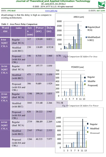
Table 3: Area Power Delay Comparison
Word
size
Adder
Are
a
(um)
Power
(uw)
Delay
(ns)
delay-power product
10-15(ws)
8-bit SQRT CSLA
Regular (dual RCA)
317 139.09 0.853 118.64
Modified (with BEC)
230 118.89 0.9218 109.6
Proposed (with HA and CBL)
146 4.510 1.060 4.78
16-bit SQRT CSLA
Regular (dual RCA)
649 197.77 1.050 207.65
Modified (with BEC)
475 175.01 1.430 250.264
Proposed (with HA and CBL)
306 9.689 1.929 18.69
32-bit SQRT CSLA
Regular (dual RCA)
1346 399.34 1.835 732.788
Modified (with BEC)
1043 331.68 2.266 751.58
Proposed (with HA and CBL)
626 20.222 3.945 79.775
64-bit SQRT CSLA
Regular (dual RCA)
2739 586.89 2.269 1331.6534
Modified (with BEC)
2165 379.61 2.555 969.9
Proposed (with HA and CBL)
1266 40.535 7.977 323.34
Fig.9 Comparison Of Adders For Area
[image:5.595.84.511.90.709.2]Fig.10 Comparison Of Adders For Power
Fig.11 Comparison Of Adders For Power-Delay Product
7. CONCLUSION:
0 500 1000 1500 2000 2500 3000
AREA (um)
Regular(dual RCA)
Modified(wit h BEC)
0 100 200 300 400 500 600 700
1 3 5 7 9 11 13
POWER (uw)
Proposed( Regular
Modifie
0 200 400 600 800 1000 1200 1400
1 3 5 7 9 11 13
Regular
Modified
A
simple
design
is
proposed
for
implementing the CSLA with the help of
half adder and common Boolean logic. It
offers the great advantage in the reduction
of area, total power and also reduces the
power delay product (PDP). From the
above data we obtained that the proposed
CSLA design on an average reduces area
by 53.5%, power by 93% and power-delay
product by 75.71%, which is a great
achievement of proposed architecture over
the existing architectures of CSLA.
Therefore this design is suitable for battery
operated processing elements.
VIII. FUTURE DEVELOPMENT:
The improvement in design will be applied
in designing ALU and Floating point unit,
VLSI architecture for lifting based
discrete wavelet transform,
High Speed
Single Precision Floating Point Unit
[7][8][9]. The same will be targeted for
specific real time low power and high
speed applications.
REFRENCES:
[1] B.Ramkumar, and Harish M Kittur,(2012) ‘Low Power Area Efficient Carry Select Adder’,IEEE Transaction on Very Large Scale Integration(VLSI) System, PP.1-5.
[2] S.Manju, V.Sornagopal,(2013) ‘An Efficient SQRT Architecture of Carry Select Adder by Common Boolean Logic’2013 IEEE
[3] B. Ramkumar, H.M. Kittur, and P. M. Kannan, “ASIC implementation of modified faster carry save adder,” Eur. J. Sci. Res., vol. 42, no. 1, pp.53–58, 2010.
[4] Y.He, C. H. Chang, and J. Gu, “An area efficient 64- bit square root carry select adder for low power application, IEEE 2005
[5] J.M. rabaey, Digital Integrated Circuits – A Design Perspective: Prentice-Hall, 2001
[6] O. J. Bedrij, “Carry-select adder,” IRE Trans. Electron. Comput., pp.340–344, 1962
[7] Ushasree G , Dhanabal r, Sarat kumar sahoo,
“Implementation of a High Speed Single Precision Floating Point Unit using Verilog”,
International Journal of Computer Applications (0975 – 8887) National conference on VSLI and Embedded systems 2013 "
[8] Dhanabal R, Bharathi V,Athmakuri Vivek, “
Design and Implementation of Low Power Floating Point Arithmetic Unit” ,International Journal of Applied Engineering Research, ISSN 0973-4562 Volume 9, Number 3 (2014) pp. 339-346.
[9] Ushasree G,Dhanabal r, Sarat kumar sahoo, “VLSI Implementation of a High Speed Single Precision Floating Point Unit Using Verilog”,