© 2017, IRJET | Impact Factor value: 5.181 | ISO 9001:2008 Certified Journal
| Page 36
DESIGN AND VERIFICATION OF PHY INTERFACE FOR PCIe GEN 3.0 AND
USB GEN 3.1 USING UVM METHODOLOGY
Richard A Prasad
1, Madhusudan Kulkarni
21
PG Scholar, Dept. of ECE, CMR Institute of Technology, Karnataka, India
2Assistant Professor, Dept. of ECE, CMR Institute of Technology, Karnataka, India
---***---Abstract -
T
he peripheral component interconnect bus(PCI) was developed in the early 90’s. The standard followed earlier was IBM’s advance Technology bus (AT), usually referred as Industry Standard Architecture Bus (ISA), IBM’s Microchannel Architecture Bus (MCA), EISA (Extended Industry Standard Architecture) and VESA (Video Electronics Standard Association). Eventually PCI became a standard peripheral bus. After few years, PCI-X (Extended) was developed followed by PCI-X 2.0. The speed ceiling and the high pin count turned the interest from parallel to serial bus model. PCIe (Peripheral Component Interconnect express) is of the third generation and supports servers, systems and mobile devices. PCIe incorporates a layered architecture consisting transaction layer, data link layer and the physical layer. It also owes much to its antecedents, PCI and PCI-X. The PHY (Physical Layer) consists of two sub-blocks logical and electrical which supports duplex communication. Logical sub block has MAC (Media Access Control), PCS (Physical Code Sublayer) and the electrical sub block has PMA (Physical Media Attachment Layer). In this thesis, the work includes, design and verification of several blocks of physical layer for PCI Express and USB. The RTL is modelled in Verilog and the same is verified in UVM (Universal Verification Methodology) environment using Questasim 10.0c from Mentor Graphics.
Key Words: PIPE,PCIe, PHY, MAC, PCS, PMA, USB, UVM.
1.
INTRODUCTION
Connecting two or more devices such as CPU, main memory and I/O devices in the system requires buses, these busses usually carry data, address and control signals. The generation of buses is as follows:
The 1st generation buses were like VESA (Video Electronics Standards Association, commonly known as VL Bus), Micro Channel buses and ISA (Industry Standard Architecture).
The 2nd generation of buses are SPI (Serial Parallel Interface), I2C (Inter Coordinated Circuit), AGP (Advanced Graphics Port), USB (Universal Serial Bus), PCI (Peripheral Component Interconnect) and PCI-X (Peripheral Component Interconnect Extended). PCI and PCI-X are also called as Parallel PCI. These 2nd generation buses have high speed, low power consumption and low cost.
The 3rd generation buses include PCIe (Peripheral Component Interconnect Express), SATA (Serial Advance technology Attachment), USB 3.0 and USB 3.1. These 3rd generation buses follow a serial lane based architecture which replaces parallel bus with serial interconnect bus. These 3rd generation I/O buses possess high performance to interconnect peripheral devices and most likely to find home in portable devices, desktop version PC’s, servers and workstations in different computing and communications levels.
Traditional PCI (Peripheral Component Interconnect) is a parallel bus specified under the PCI local bus group of standards. It is typically used by the system architects to interconnect peripherals or add optional add-on cards to systems using PCI plug-in cards with PCI slots provided on the motherboard.
PCIe (Peripheral Component Interconnect Express) is an industry standard serial bus protocol that offers high bandwidth communication links from computing, embedded processors to endpoint peripherals like Ethernet, USB, storage and other type peripherals. It offers fewer upgrades to the specifications that went before it like PCI and PCI-X. By moving to a serial interface, fewer pins are required for a PCIe connection than the previously required, PCI and PCI-X.
1.1 Benefits of Serial Bus
© 2017, IRJET | Impact Factor value: 5.181 | ISO 9001:2008 Certified Journal
| Page 37
1.2 What is PHY?
[image:2.595.313.556.102.230.2]PHY (Physical Layer Interface) is an acronym for physical layer of OSI model required to implement physical layer functions. The interface between the link layer, MAC and any physical medium like fiber optics or copper cable is connected through PHY. It distinctively includes Physical Coding Sub layer (PCS) and Physical Medium Attachment layer (PMA).
Fig -1: Partitioned physical layer for PCIe
2. PHY LAYER OF PCI EXPRESS
The PHY layer of PCI Express administrates low level PCIe protocol and signaling including features like serialization and deserialization of data, encoding/decoding (128b/130b), 8 GTps, receiver recognition and elastic/analog buffers. The foremost concern of PHY is modifying data clock domain of
PCIe rate well matched with general logic of ASIC.The PHY
layer has all the necessary circuits for operating the interface, it includes like input buffer, drivers, parallel/ serial to serial/parallel converters, phase lock loops and impedance matching circuits. Through a very specific format data exchange takes place between the physical and data link layer. This layer serializes the received data from data link layer and transmits the same over the PCIe link with compatible width and frequency of device on different side of the link.
3. PROJECT DESIGN AND METHODOLOGY
[image:2.595.39.284.219.364.2]This thesis mainly involves the designing and verifying/validating of physical layer (PHY) interface for PCIe and USB. The PHY layer we are designing is compatible for PCIe generation 3.0 and USB version 3.1. The document includes the top level of PHY design from verification IP. The diagram below shows the basic architecture block of the design (Physical Layer).
Fig -2: Partitioned physical layer for PCIe
Main modules in the design are SERDES comprising parameterized data (8/16/32) width, clock generation circuitry, encoding/decoding module and byte separator. There’s quite a few components or IC’s between CPU and PCIe interface collectively referred as root complex (RC). The interface between CPU and PCIe busses may contain several components or chips. Collectively this group is referred to as root complex (RC or root). RC usually inherent at root of the inverted PCIe tree topology. Devices in topology of PCIe that are neither switches nor bridges but perform as initiators and completers of transactions on the respective buses. Endpoints usually inherent at the
3.1
Physical Coding Sublayer
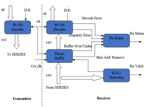
Fig -3: PCS Block Diagram
Lane to lane deskew LTSSM and are the subsections blocks of media access control layer. 8b/10b encoder/decoder, elastic buffer and receiver detection are the subsections blocks of physical coding sublayer. Analog buffers, SEDRES block, 10-bit interface unit are the subsections blocks of
physical media attachment layer. The above diagram is
[image:2.595.309.557.443.627.2]© 2017, IRJET | Impact Factor value: 5.181 | ISO 9001:2008 Certified Journal
| Page 38
decoder. PCS endorses PHY/MAC Interface as well asinterface between PCS and the PMA. Internal bit rate clocks are generated by reference input clock CLK for PCI Express transactions. Data or control character are fed to the 8B/10B encoder, the current RD (running disparity), and the TxDataK signal is needed to encode data character and control character respectively. To process the incoming data the transmitter and the receivers clock frequency should be in synchronization, these shallow variations are indemnified via elastic buffers.
3.2 Physical Media Attachment Layer
[image:3.595.310.561.125.352.2]The PMA furnishes medium-independent technique for PCS for serialization and deploy physical media. The service interface is responsible for mapping the transmit, receive group between PCS and PMA.
Fig -4: PMA Block Diagram
SERDES functionality and clock recuperation from the code-group provided by the PMD (Physical Media Dependent)
layer.The Physical Media Attachment (PMA) Layer includes
high-speed analog and digital circuitry for PCI Express signaling, also includes differential drivers and receivers for on lane in a link. Serial transmission takes place over the link and there’s a 10-bit parallel implementation-specific interface between PCS and PMA. PMA Consists analog buffers, high speed SERDES (Serialization and De-Serialization) logic creating serial data stream for PCIe, CDR (Clock Data Recovery) wilt PLL and 10-bit interface. Also includes LTSSM (Link Training Static State Machine) required for initializing lanes across links. The above diagram shows the basic PMA block with its internal sub-blocks and architecture.
[image:3.595.39.285.317.538.2]3.3 PHY Loopback Verification
Fig -5: UVM Verification Environment for PHY (Loopback)
For chips to interconnect and communicate with each other many techniques have been established. Some techniques are standardized and some are not. To test, debug, fault isolate and analog or digital validate the loopback (back to back) architecture is used. This loopback is controlled and repeatable at physical layer. loopback is a process where two chips are interconnected and are in a loop and the transmission of signals takes place via in-band interconnects. The input TxData of PHY 1 Top is verified at the output of RxData of PHY 2 Top and the same with TxData of PHY 2 is verified with the RxData of PHY 1. A test bench in UVM environment is built which in turn acts as a MAC (Media Access Control) controlling the PHY (Physical Layer).
3.4 UVM (Universal Verification Methodology)
© 2017, IRJET | Impact Factor value: 5.181 | ISO 9001:2008 Certified Journal
| Page 39
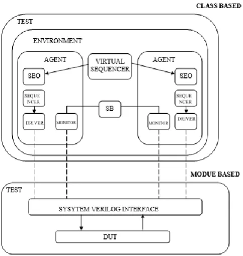
Fig -6: UVM Block Level Architecture and Test-BenchUVM test-benches are built from classes derived from the UVM component base class. Collection of verification components are reused, when used in the same or different projects they are usually called vertical and horizontal reuse respectively. Frequently reused components are agent and environment.
4. RESULTS
4.1 The 8B/10B Encoder Output
Fig -7: Input/output PHY 1 Encoder
Fig -8: Input/output of PHY 2 Encoder
4.2 The 10B/8B Decoder Output
Fig -9: Input/output of PHY 1 Decoder
[image:4.595.305.572.368.459.2]
Fig -10: Input/output of PHY 2 Decoder
4.3 SERDES Output
Fig -11: Input/output of PHY 1 SERDES
Fig -12: Input/output of PHY 2 SERDES
4.4 PHY Loopback Output
[image:4.595.39.562.476.742.2]© 2017, IRJET | Impact Factor value: 5.181 | ISO 9001:2008 Certified Journal
| Page 40
5. CONCLUSIONS
Designing PCS, PMA and various functional sub-blocks of Physical Layer for PCI Express 3.0 and USB 3.1 has been presented in this paper. The serial data transmission technology makes PCIe further consistent and scalable with very less interference to noise. Improving transfer rate results in improving the overall performance of the system. The 8-bit and data/control character is successfully encoded to 10-bit symbols thru encoder/decoder and inacceptable data is been detected by the encoder.
The underflow and overflow conditions of FIFO are sensed by elastic buffer. SKP symbols are added and removed to the half-filled buffer to maintain the half-filed state. Data loss is evaded by proper synchronization thru Elastic Buffer.
8-bit character, data and control signals are decoded to 10-bit symbols via 8b/10b decoder. Through the received data validity disparity and decoder errors are known. Major future developments are usually carried over in PCS of physical layer. Many such developments were made after the first versions of PCI express. PCIe of 3.0 generation uses 128b/130b instead 8b/10b encoding scheme, practically overcoming maximum overhead in PCI Express 1.0 versions. Point-to-point interconnect has limited electrical load on link permitting frequencies of transmission/reception to scale higher. Systems like “Always-on" are supported by hot Plug/hot Swap.
REFERENCES
[1] Jackson, Mike, and Ravi Budruk. “PCI Express
Technology: Comprehensive Guide to Generations 1.x, 2.x and 3.0”. MindShare Press, 2012.
[2] Dave Dzatko. “PCI Express PIPE Overview”, Mindshare,
Inc. March, 2004.
[3] Ravi Budruk, “An Introduction to PCI Express”,
Mindshare.
[4] Rockrohr, J. D., Mohammad, A., Ogilvie, C. R., Dramstad,
K., Sorna, M. A., Mechler, J. T., & Stauffer, “High Speed Serdes Devices and Applications”. Springer US. 2009.
[5] “LatticeECP2M PCS PIPE IP Core”, Lattice
Semiconductor. March, 2009.
[6] Priyanka M. Zade, Prachi Pendke, Shubhangini Ugale.
“Design of The Physical Layer of PCI Express- A Review”. IJAICT Volume 1, Issue 7, November 2014.
[7] Ankita R. Tembhare, Dr.Pramod B. Patil. “Design &
Implementation of PCI Express BUS Physical layer using VHDL”. International Journal on Recent and Innovation
Trends in Computing and Communication Volume: 2 Issue: 7, July 2014.
[8] Chandana K N, Karunavathi R K. “Link Initialization and
Training in MAC Layer of PCIe 3.0”. International Journal of Computer Science and Information Technologies, Vol. 6, 2015.
[9] PCI Express Base Specification, Rev. 3.0, PCI-SIG,
November 4, 2010.
[10]PCI Express Expert Core Refrence Manual, Ver. 1.6.0,
PLDApplications, February, 2006.
[11]PHY Interface for the PCI Express, SATA and USB 3.1
Architectures, Ver. 4.4.1, Intel Corporation, 2016.
[12]SystemVerilog 3.1a Language Reference Manual,
Accellara - Extensions to Verilog-2001, 2004.
[13]Universal Verification Methodology (UVM), User’s Guide
- 1.1, Acellera, 2011.
[14]“Welcome to PCI-SIG | PCI-SIG.” Welcome to PCI-SIG
PCI-SIG, www.pcisig.com/.
BIOGRAPHIES
RICHARD A PRASAD Is pursuing his MTech in VLSI Design and Embedded System in CMR Institute
of Technology, Visvesvaraya