N A N O E X P R E S S
Open Access
Electrical Properties of Midwave and
Longwave InAs/GaSb Superlattices
Grown on GaAs Substrates by
Molecular Beam Epitaxy
D. Benyahia
1*,
Ł
. Kubiszyn
2, K. Michalczewski
1, J. Boguski
1, A. K
ę
b
ł
owski
2, P. Martyniuk
1, J. Piotrowski
2and A. Rogalski
1Abstract
In the present work, we report on the in-plane electrical transport properties of midwave (MWIR) and longwave infrared (LWIR) InAs/GaSb type-II superlattices (T2SLs) grown by molecular beam epitaxy (MBE) system on GaAs (001) substrate. The huge lattice mismatch between the T2SL and GaAs substrate is reduced by the growth of GaSb buffer layer based on interfacial misfit array (IMF) technique. In order to compensate the strain in the InAs/GaSb T2SL, we utilized a special shutters sequence to get InSb-like and GaAs-like interfaces. It is found that the MWIR InAs/GaSb T2SL exhibits a p- and n-type conduction at low and high temperatures, respectively. Interestingly, the conduction change temperature is observed to be dependent on the growth temperature. On the other hand, LWIR T2SL conduction is dominated only by electrons. It is important to note that the dominant scattering mechanism in LWIR T2SL at low temperatures is the interface roughness scattering mechanism.
Keywords:Molecular beam epitaxy, Type-II superlattices, Hall effect, High-resolution X-ray diffraction
Background
Since InAs/GaSb T2SL has been conceptualized by Sai-Halasz et al. [1] in 1977, great attentions have been paid in the investigation of this semiconductor material. Photodetectors based on this T2SL present theoretically higher potential over mercury cadmium telluride (HgCdTe) and the state-of-the-art infrared material sys-tems for the next generation of infrared (IR) applications [2,3]. Interestingly, InAs/GaSb T2SL exhibits an unusual type-II broken gap band lineup where the InAs conduc-tion band minimum is located 140 meV lower than the GaSb valence band top [1]. Consequently, the funda-mental transition between the heavy-hole subbands and the conduction band bottom depends on the thickness of the InAs or GaSb layer [4]. However, the main advan-tage of this alignment is the reduction of Auger recom-bination rate thanks to the suppression of some
non-radiative pathways in the valence band [5]. In addition, the band-to-band tunneling is decreased sig-nificantly due to the large effective masses (≈0.04m0) of electrons and holes [6]. These two latter features permit the reduction of the dark current, which leads to the high operation temperature (HOT) of the photodetector. InAs/GaSb T2SL is traditionally grown on lattice-matched GaSb substrate. However, this latter is expensive and avail-able in small sizes less than 3 in., which impede the realization of large-format focal plane arrays (FPAs). More-over, GaSb substrates are not “epi-ready” and their growth surfaces contain many macroscopic defects [7]. Further-more, the absorption coefficient is relatively high in GaSb substrate (≈100 cm−1) for IR radiation above 5μm [8]. Due to its numerous advantages, GaAs has been proposed as a viable candidate for the growth of InAs/GaSb T2SL [9–12]. Indeed, they are“epi-ready,” cost-efficient, and available in large sizes up to 6 in. Besides, GaAs has an absorption coef-ficient two orders of magnitude lower than that of GaSb. Unfortunately, a huge lattice mismatch (~ 7.5%) exists be-tween GaAs and InAs/GaSb T2SL that results in high misfit
* Correspondence:[email protected]
1Institute of Applied Physics, Military University of Technology, 2 Witold
Urbanowicz Str., 00-908 Warsaw, Poland
Full list of author information is available at the end of the article
dislocation density (109cm−2) [13]. Therefore, it is com-pulsory to concept new growth techniques to relieve the strain and reduce the dislocation density. Among these techniques are low-temperature nucleation [14] and IMF technique [15,16].
In order to improve the performances of photodetec-tors based on InAs/GaSb T2SL, a better understanding of fundamental parameters is needed. One of these pa-rameters is the background carrier concentration which is associated with the minority carrier lifetime and diffu-sion lengths. It is worth noting that InAs and GaSb bulk materials have opposite polarity of carriers’ concentra-tion. Indeed, InAs and GaSb materials grown using mo-lecular beam epitaxy (MBE) are residuallyn- andp-type, respectively [17, 18]. Consequently, the conduction of the InAs/GaSb T2SL is predicted to be dependent on the thickness of each constituent.
In this paper, we investigate the in-plane transport properties of 10 ML InAs/10 ML GaSb and 24 ML InAs/7 ML GaSb T2SLs dedicated for the detection in MWIR and LWIR regions, respectively, grown on semi-insulating GaAs (001) substrates. This study is achieved by performing a temperature-dependent Hall effect measurement using the Van der Pauw method. Besides, the influence of the growth temperature on the conduction of the InAs/GaSb T2SL is presented.
Methods
InAs/GaSb T2SL samples have been grown on semi-insulating GaAs (001) substrates in a RIBER Com-pact 21-DZ solid source MBE system. This latter is equipped with standard effusion cells for group III ele-ments (indium (In) and gallium (Ga)) and valved cracked cells for group V materials (arsenic (As) and antimony (Sb)). The cracker temperatures were kept at 900 °C for both As and Sb to produce As2 and Sb2, respectively. The manipulator thermocouple (TC) and BandiT (BT) are utilized to monitor the growth temperature. This lat-ter has been calibrated from the GaAs oxide desorption temperature. Following the deoxidization of GaAs sub-strates at 610 °C (measured by BT), a 250-nm-thick GaAs layer was deposited at 585 °C (BT) to get a smooth starting surface. Subsequently, a 1-μm-thick GaSb buffer layer has been grown using IMF technique at a BT temperature of 440 °C [16, 19]. This technique consists on the formation of a periodic array of 90° misfit tion at the GaAs/GaSb interface leading to a low disloca-tion density (≈106cm−2) [20]. After the growth of GaSb buffer layer, the BT cannot be used anymore due to the emissivity changes, surface roughening, and extra radia-tive absorption mechanisms [21]. Thus, the growth temperature of the InAs/GaSb T2SL is controlled only by the TC. MWIR 10 ML InAs/10 ML GaSb T2SLs are grown at different substrate temperatures, 330, 390, and
400 °C (TC) to investigate the influence of the growth temperature on the transport properties. On the other hand, LWIR 24 ML InAs/7 ML GaSb T2SL has been de-posited at only 390 °C. In order to compensate the strain between InAs and GaSb, special shutters sequence, which was reported to lead to a better structural quality [22, 23], was used as follows: growth of InAs was followed by Sb soak of 8 s to form InSb-like bonds, whereas GaSb growth was followed by 2 s of As soak to grow GaAs-like interface. The V/III flux ratio is 8.3 and 4.6 for InAs and GaSb, respectively. Besides, the growth rate is 0.5 ML/s for both InAs and GaSb. The growth was monitored in situ by reflection high-energy electron diffraction (RHEED) system.
The grown samples have been assessed by high-resolution X-ray diffraction (HRXRD) of PANalytical X’Pert to investigate the structural properties. The Cu Kα1 radiation (λ≈1.5406 Å) originating from a line focus and a four bounce Ge (004) monochromator have been utilized. The transport properties were evaluated by Hall effect mea-surements using the Van der Pauw method in an ECOPIA system, with a temperature range of 80–300 K. Measure-ments were performed on square samples of 6 × 6 mm2; contact was made by indium dots in each corner. A mag-netic field of 0.4 T was applied normal to the samples.
Results and Discussion
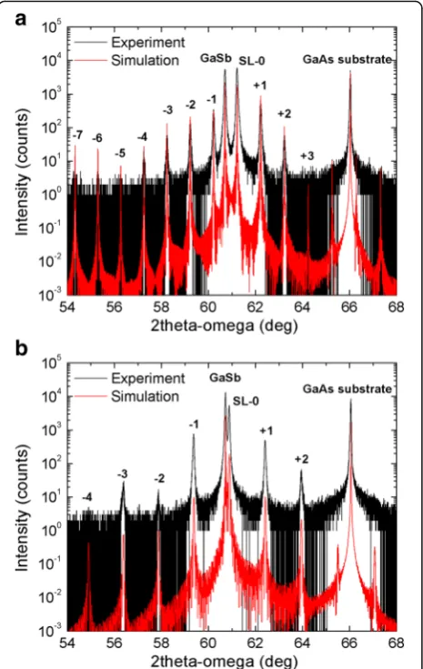
Figure1illustrates the measured and simulated HRXRD 2θ-ω scanning curves of the symmetric (004) reflection for the MWIR and LWIR InAs/GaSb T2SLs. The simu-lation is performed by the “Epitaxy” software provided by PANalytical X’Pert. As can be seen, there are well-resolved satellites with an order up to 4 for MWIR T2SL and up to 7 for LWIR one. This indicates the high structural quality of the grown layers, especially for LWIR T2SL. On the other hand, the full width at half maximum (FWHM) of the zeroth-order peak measured in ω-2θ direction is 107 and 99 arcsec for MWIR and LWIR T2SLs, respectively. The superlattice period (L) is determined from the angle distance between two adjacent satellites (Δθ) as follows:
L¼λ=ð2Δθ cosθSLÞ ð1Þ
thicknesses of LWIR T2SL constituents are as follows: GaSb 2.3 nm (7.5 ML), GaAs 0.1 nm (0.2 ML), InAs 7.4 nm (24.7 ML), and InSb 0.4 nm (1 ML). The lattice mismatch determined from the angle between the zeroth-order peak and the GaSb buffer layer is 8.9 × 10⁻³ and 4.5 × 10⁻³for MWIR and LWIR T2SLs, respectively. Figure2 presents the asymmetric (115) reciprocal space map (RSM) for the grown T2SLs. In both samples, the satellites of the superlattices and the GaSb peak are aligned vertically (they have the same component of the scattering vector Qx), which leads to the conclusion that both T2SLs are practically fully strained.
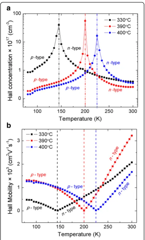
The in-plane electrical parameters of the grown MWIR InAs/GaSb T2SLs are illustrated in Fig. 3. As it
can be seen, the unintentionally doped InAs/GaSb T2SL exhibits a reproducible change in type of conductivity. In spite of the influence of GaSb buffer layer (p-type) on the Hall effect measurements, it should be noted that the change in the conductivity type is due only to the T2SL layer. This change was also reported by several groups [6, 24–26]. The T2SL exhibits a p-type conduc-tion below the temperature at which the change occurs (Tch) and ann-type conduction aboveTch. As mentioned previously, the InAs and GaSb layers exhibit an n-type and p-type conduction, respectively. Therefore, the re-sidual background of the InAs/GaSb T2SL with similar thickness for the two constituents is induced by the ma-jority carrier compensation from the binary constituents of the T2SL [27]. For the value ofTch, Mohseni et al. [6] reported a value of 140 K, Christol et al. [24] got a value of 190 K, while Khoshakhlagh et al. [25] pointed out a value of 200 K. The behavior of the sheet carrier concen-tration and mobility is governed by the well-known in-trinsic phonon scattering (acoustic, piezoelectric, polar, and nonpolar optical) mechanisms. Exceptionally, the Hall mobility increases with increase of the temperature above Tch (Fig. 3b); this is probably because of the ion-ized traps due to the InSb interface at the GaSb-on-InAs interface [6]. Tch value is 145, 195, and 225 K, for the T2SL grown at 330, 390, and 400 °C, respectively (Fig.3); this is due probably to the high hole concentration at higher growth temperature, which shifts theTchto lower temperature. The high hole concentration is due to de-fects and ionized vacancies at high growth temperature. The InAs/GaSb T2SL grown at 390 °C is characterized by a carrier’s concentration of 1.8 × 10¹⁶and 2.5 × 1016cm−3 at 80 and 300 K, respectively. This result is better than that reported by Mohseni et al. [6] (Hall concentration ranges from 1.5 to 4 × 1017cm−3) and practically the same as that reported by Christol et al. [24] (Hall concentration of 1.6 × 10¹⁶and 6 × 1016cm−3at 100 and 300 K, respect-ively). On the other hand, the Hall mobility is 1300 (p-type) and 3200 cm2/V s (n-type), at 80 and 300 K, re-spectively. The reached mobility is much higher than that reported by Christol et al. [24], who got a Hall mobility of 100 and 1800 cm2/V s at 100 and 300 K, respectively.
The resistivity of the three different samples is shown in Fig. 4. It can be noticed that the resistivity and temperature have two well-defined slopes. For each sam-ple, two thermal activation energies can be extracted from the Arrhenius law. For then-type region, the acti-vation energy Ean is 58, 72, and 68 meV for the T2SL grown at 330, 390, and 400 °C, respectively. While for the p-type region, Eapis equal to 7, 12, and 14 meV, for the InAs/GaSb T2SL deposited at 330, 390, and 400 °C, respectively. For low temperatures (belowTch), the T2SL shows a p-type due to p-type carriers associated with Eap which dominate the carrier generation and Fig. 1HRXRD 0042θ-ωscan ofaMWIRband LWIR InAs/GaSb T2SLs.
[image:3.595.58.291.88.456.2]recombination mechanisms. For temperatures aboveTch, the T2SL exhibits ann-type conduction due to the acti-vation of deep-level carriers associated with high activa-tion energy Ean. The source of these deep levels is the shallow levels in the bulk InAs that is the result of the band lineup between InAs and InAs/GaSb T2SL and which acts as deep levels in the InAs/GaSb T2SL [28].
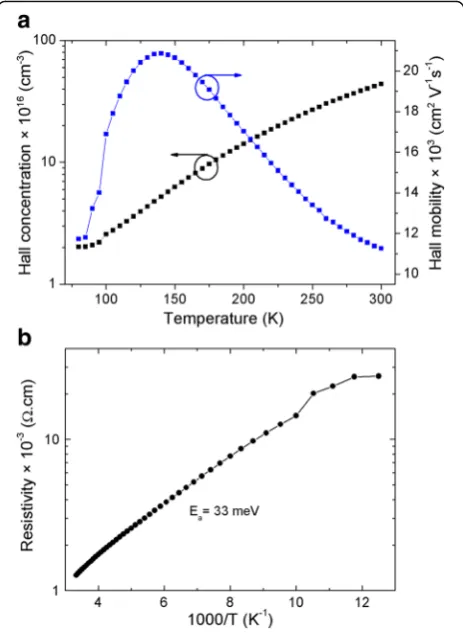
The Hall concentration, mobility, and resistivity of the LWIR InAs/GaSb T2SL are presented in Fig.5. Opposite to the MWIR T2SL, there is no change of type of con-ductivity in the case of this sample. This T2SL exhibits ann-type conduction. The influence of thep-type GaSb buffer (low-mobility carriers) layer on the Hall effect measurement for this n-type T2SL (high-mobility car-riers) is negligible, since the Hall mobility is proportional to the carriers’ mobility squared. Khoshakhlagh et al. [25] reported the same result for 13 ML InAs/7 ML GaSb T2SL. In addition, Szmulowicz et al. [29] pointed out that LWIR T2SL, in which the InAs layer is thicker than GaSb, tends to ben-type. Thisn-type conduction is due to the large thickness of InAs layer (residually n-doped.) compared to that of GaSb. These n-type car-riers are associated with an activation energy of 33 meV
(Fig. 5b). The behavior of the Hall concentration and mobility is typical for n-type semiconductors, except the temperature range below 95 K, where the carrier’s
concentration and mobility are almost
temperature-independent. This is an indication of the existence of a temperature-independent scattering mechanism in this temperature region. This latter is demonstrated to be the interface roughness scattering (IRS) mechanism [30–34]. This mechanism is dominant at low temperature, where the phonon scattering is fro-zen out [35]. IRS mechanism is due to the existence of interfaces, as well as the variation of the layers’ thick-nesses, which results in the variation of the electronic energy levels; therefore, they act as a source of carrier scattering [35]. Moreover, the Hall mobility dominated by the IRS mechanism is proportional to the sixth power of the InAs thickness (μ∝d6InAs:2 ) [35].
Conclusions
In summary, InAs/GaSb T2SLs have been grown on GaAs substrate using GaSb buffer layer based on IMF technique. Moreover, these T2SLs have been Fig. 2Asymmetric 115 RSM ofaMWIR andbLWIR InAs/GaSb T2SLs. The reciprocal space map for the asymmetric reflection (115) ofaMWIR and
bLWIR InAs/GaSb T2SLs. The peaks in both superlattices are aligned vertically (they have the same value of the scattering vector Qx). Therefore,
[image:4.595.59.539.87.407.2]demonstrated for MWIR and LWIR detection regions. It has been found that MWIR T2SL exhibits a change in the conduction type, form p- to n-type as the temperature increases. Furthermore, the temperature at which the change occurs increases as the growth temperature of the T2SLs increases. This conduction type change is attributed to the existence of two impur-ity levels with two different activation energies. On the other hand, the LWIR InAs/GaSb T2SL conduction is demonstrated to be n-type for the whole range of
Fig. 3aHall concentration andbHall mobility of MWIR InAs/GaSb T2SL grown at different temperatures. The electrical parameters of the MWIR InAs/GaSb T2SLs grown at different temperatures.aHall concentration: the three T2SLs exhibit a change of conductivity. They arep-type at low temperatures andn-type at high temperatures.bHall mobility: there are two regions for the mobility tendency. For low temperature, the mobility decreases due to the different scattering mechanisms. For high temperatures, the mobility increases by increasing the temperature, which can be explained by the ionized traps in InSb-like interface. The temperature at which the conductivity change occurs increases when the growth temperature increases, which is due to the high defect levels at higher temperatures
Fig. 4Hall resistivity of the MWIR InAs/GaSb T2SL grown ata330 °C,
b390 °C, andc400 °C. The Hall resistivity of the MWIR InAs/GaSb T2SL deposited at different growth temperatures,a330 °C,b390 °C, andc400 °C. For each graph, there are two well-defined slopes. From the Arrhenius law, two thermal energies can be extracted, which confirms the existence of two impurity levels. One represents the
[image:5.595.311.539.84.614.2] [image:5.595.56.292.85.475.2]temperature. In addition to the conventional scattering mechanisms, the IRS mechanism is proved to be the dominant scattering mechanism at low temperatures. These results allow a better understanding of the phys-ical properties of the InAs/GaSb T2SL, which leads to the improvement of IR photodetector performances based on this material.
Abbreviations
BT:BandiT; FPAs: Focal plane arrays; FWHM: Full width at half maximum; HOT: High operation temperature; HRXRD: High-resolution X-ray diffraction; IMF: Interfacial misfit array; IR: Infrared; IRS: Interface roughness scattering; LWIR: Longwave infrared; MBE: Molecular beam epitaxy; MWIR: Midwave infrared; RHEED: Reflection high-energy electron diffraction; RSM: Reciprocal space map; T2SL: Type-II superlattice; TC: Thermocouple
Acknowledgements
This paper has been completed with the financial support of the Polish National Science Centre: grant no.: OPUS/UMO-2015/19/B/ST7/02200.
Funding
The source of funding of this paper is the grant no.: OPUS/UMO-2015/19/B/ ST7/02200.
Availability of Data and Materials
The conclusions made in this manuscript are based on the data (main text and figures) presented and shown in this paper.
Authors’Contributions
DB grew the samples, made the HRXRD and Hall effect characterization, and wrote the manuscript.ŁK, KM, JB, and AK contributed on the design and MBE growth of the grown samples. PM, JP, and AR helped in the theoretical analysis and the interpretation of the results. All authors read and approved the final manuscript.
Competing Interests
The authors declare that they have no competing interests.
Publisher’s Note
Springer Nature remains neutral with regard to jurisdictional claims in published maps and institutional affiliations.
Author details 1
Institute of Applied Physics, Military University of Technology, 2 Witold Urbanowicz Str., 00-908 Warsaw, Poland.2Vigo System S.A., 129/133 Poznańska Str., 05-850 Ożarów Mazowiecki, Poland.
Received: 24 May 2018 Accepted: 25 June 2018
References
1. Sai-Halasz GA, Tsu R, Esaki L (1977) A new semiconductor superlattice. Appl Phys Lett 30(12):651–653
2. Razeghi M, Nguyen BM, Delaunay PY, Huang EK, Pour SA, Manukar P, Bogdanov S. State-of-the-art type II antimonide-based superlattice photodiodes for infrared detection and imaging. Nanophoton Macrophoton Space Environ III, Proc of SPIE 2009;7467:74670T-746701
3. Plis EA (2014) InAs/GaSb type-II superlattice detectors. Adv Electron 2014:1–12 4. Rodriguez JB, Christol P, Cerutti L, Chevrier F, Joullié A (2005) MBE growth
and characterization of type-II InAs/GaSb superlattices for mid-infrared detection. J Cryst Growth 274(1):6–13
5. Grein CH, Cruz H, Flatté ME, Ehrenreich H (1994) Theoretical performance of very long wavelength InAs/InxGa1−xSb superlattice based infrared detectors.
Appl Phys Lett 65(20):2530–2532
6. Mohseni H, Litvinov VI, Razeghi M (1998) Interface-induced suppression of the Auger recombination in type-II InAs/GaSb superlattices. Phys Rev B 58(23):15378–15380
7. Plis E, Rodriguez JB, Balakrishnan G, Sharma YD, Kim HS, Rotter T, Krishna S (2010) Mid-infrared InAs/GaSb strained layer superlattice detectors with nBn design grown on a GaAs substrate. Semicond Sci Technol 25(8):085010 8. Chandola A, Pino R, Dutta PS (2005) Below bandgap optical absorption in
tellurium-doped GaSb. Semicond Sci Technol 20(8):886–893
9. Tang B, Xu Y-Q, Zhou Z-Q, Hao R-T, Wang G-W, Ren Z-W, Niu Z-C (2009) GaAs based InAs/GaSb superlattice short wavelength infrared detectors grown by molecular beam epitaxy. Chin Phys Lett 26(2):028102 10. Nguyen B-M, Hoffman D, Huang EK, Bogdanov S, Delaunay P-Y, Razeghi M,
Tidrow M (2009) Demonstration of midinfrared type-II InAs/GaSb superlattice photodiodes grown on GaAs substrate. Appl Phys Lett 94(22): 223506
11. Zhang XB, Ryou JH, Dupuis RD, Petschke A, Mou S, Chuang SL, Xu C, Hsieh KC (2006) Metalorganic chemical vapor deposition growth of high-quality InAs∕GaSb type II superlattices on (001) GaAs substrates. Appl Phys Lett 88(7):072104
12. Benyahia D, KubiszynŁ, Michalczewski K, Kębłowski A, Martyniuk P, Piotrowski J, Rogalski A (2017) Comparative study of the molecular beam epitaxial growth of InAs/GaSb superlattices on GaAs and GaSb substrates. Acta Phys Pol A 132(2):322–324
[image:6.595.58.290.88.405.2]13. Johnson GR, Cavenett BC, Kerr TM, Kirby PB, Wood CEC (1988) Optical, Hall and cyclotron resonance measurements of GaSb grown by molecular beam epitaxy. Semicond Sci Technol 3(12):1157
14. Michel E, Mohseni H, Kim JD, Wojkowski J, Sandven J, Xu J, Razeghi M, Bredthauer R, Vu P, Mitchel W, Ahoujja M (1997) High carrier lifetime InSb grown on GaAs substrates. Appl Phys Lett 71(8):1071–1073
15. Huang SH, Balakrishnan G, Khoshakhlagh A, Jallipalli A, Dawson LR, Huffaker DL (2006) Strain relief by periodic misfit arrays for low defect density GaSb on GaAs. Appl Phys Lett 88(13):131911
16. Benyahia D, KubiszynŁ, Michalczewski K, Kębłowski A, Martyniuk P, Piotrowski J, Rogalski A (2018) Interfacial misfit array technique for GaSb growth on GaAs (001) substrate by molecular beam epitaxy. J Electron Mater 47(1):299–304
17. Benyahia D, KubiszynŁ, Michalczewski K, Kębłowski A, Martyniuk P, Piotrowski J, Rogalski A (2016) Low-temperature growth of GaSb epilayers on GaAs (001) by molecular beam epitaxy. Opto-Electron Rev 24(1):40–45 18. Benyahia D, KubiszynŁ, Michalczewski K, Kębłowski A, Martyniuk P, Piotrowski
J, Rogalski A (2016) Molecular beam epitaxial growth and characterization of InAs layers on GaAs (001) substrate. Opt Quant Electron 48(9):428
19. Benyahia D, KubiszynŁ, Michalczewski K, Kębłowski A, Martyniuk P, Piotrowski J, Rogalski A (2018) Optimization of the interfacial misfit array growth mode of GaSb epilayers on GaAs substrate. J Cryst Growth 483:26–30
20. Balakrishnan G, Tatebayashi J, Khoshakhlagh A, Huang SH, Jallipalli A, Dawson LR, Huffaker DL (2006) III/V ratio based selectivity between strained Stranski-Krastanov and strain-free GaSb quantum dots on GaAs. Appl Phys Lett 89(16):161104
21. Shanabrook BV (1993) Variations in substrate temperature induced by molecular-beam epitaxial growth on radiatively heated substrates. J Vac Sci Technol B 11(3):994
22. Jasik A, Sankowska I, Pierścińska D, Regiński K, Pierściński K, Kubacka-Traczyk J (2011) Blueshift of bandgap energy and reduction of non-radiative defect density due to precise control of InAs-on-GaSb interface in type-II InAs/ GaSb superlattice. J Appl Phys 110(12):123103
23. Plis A, Annamalai S, Posani KT, Krishna S, Rupani RA, Ghosh S (2006) Midwave infrared type-II InAs/GaSb superlattice detectors with mixed interfaces. J Appl Phys 100(1):014510
24. Christol P, Konczewicz L, Cuminal Y, Aït-Kaci H, Rodriguez JB, Joullié A (2007) Electrical properties of short period InAs/GaSb superlattice. Phys Status Solidi C 4(4):1494–1498
25. Khoshakhlagh A, Jaeckel F, Hains C, Rodriguez JB, Dawson LR, Malloy K, Krishna S (2010) Background carrier concentration in midwave and longwave InAs/GaSb type II superlattices on GaAs substrate. Appl Phys Lett 97(5):051109
26. Haugan HJ, Brown GJ, Szmulowicz F, Grazulis L, Mitchel WC, Elhamri S, Mitchell WD (2005) InAs/GaSb type-II superlattices for high performance mid-infrared detectors. J Cryst Growth 278(1):198–202
27. Hood A, Razeghi M, Aifer EH, Brown GJ (2005) On the performance and surface passivation of type II InAs∕GaSb superlattice photodiodes for the very-long-wavelength infrared. Appl Phys Lett 87(15):151113
28. Shen J, Ren SY, Dow JD (1992) Deep levels in type-II InAs/GaSb superlattices. Phys Rev B 46(11):6938–6946
29. Szmulowicz F, Elhamri S, Haugan HJ, Brown GJ, Mitchel WC (2009) Carrier mobility as a function of carrier density in type-II InAs/GaSb superlattices. J Appl Phys 105(7):074303
30. Sakaki H, Noda T, Hirakawa K, Tanaka M, Matsusue T (1987) Interface roughness scattering in GaAs/AlAs quantum wells. Appl Phys Lett 51(23):1934–1936 31. Gottinger R, Gold A, Abstreiter G, Weimann G, Schlapp W (1988) Interface
roughness scattering and electron mobilities in thin GaAs quantum wells. EPL Europhys Lett 6(2):183
32. Meyer JR, Arnold DJ, Hoffman CA, Bartoli FJ, Ram-Mohan LR (1992) Electron and hole in-plane mobilities in HgTe-CdTe superlattices. Phys Rev B 46(7): 4139–4146
33. Hoffman CA, Meyer JR, Youngdale ER, Bartoli FJ, Miles RH (1993) Interface roughness scattering in semiconducting and semimetallic InAs-Ga1−xInxSb
superlattices. Appl Phys Lett 63(16):2210–2212
34. Szmulowicz F, Elhamri S, Haugan HJ, Brown GJ, Mitchel WC (2007) Demonstration of interface-scattering-limited electron mobilities in InAs∕GaSb superlattices. J Appl Phys 101(4):043706