Please cite this article as: H. Gholamalitabar, J. Adabi, M. Rezanejad, A High Gain Bipolar Pulse Generator with Low Voltage Input Source, International Journal of Engineering (IJE), IJE TRANSACTIONS B: Applications Vol. 32, No. 8, (August 2019) 1126-1133
International Journal of Engineering
J o u r n a l H o m e p a g e : w w w . i j e . i rA High Gain Bipolar Pulse Generator with Low Voltage Input Source
H. Gholamalitabara, J. Adabi*a, M. Rezanejadb
a Department of Electrical and Computer Engineering,Babol Noshirvani University of Technology, Babol, Iran b Department of Electrical and Computer Engineering, University of Mazandaran, Babolsar, Iran
P A P E R I N F O
Paper history: Received 30 May 2019
Received in revised form 21 July 2019 Accepted 28 July 2019
Keywords:
Bipolar Pulsed Power Generator Switched-Capacitor
Modular Marx Generator
A B S T R A C T
This paper proposes a pulsed power generator which consists of two types of switched-capacitor booster modules. A doubling mode module employed to elevate the input voltage to a specified level and, constant mode module is used to increase the elevated voltage into the finally intended bipolar output voltage. Also, the proposed modular structure does not utilize any switches across the load. Other advantage of the proposed structure is its lower current stress on source and every circuit component near it. In comparison with Marx Generator (MG) based topologies, the number of circuit components has been significantly reduced, which led to cost-saving and prevention of circuit control complexity. Calculation of the capacitors is presented. Experimental tests and simulations are performed on a five-module system which confirms the high performance of the proposed topology.
doi: 10.5829/ije.2019.32.08b.08
1. INTRODUCTION1
The major concept of the pulsed power technology is receiving energy from input sources, storing it in energy storage components and generating high voltage/current pulses for the loads which requires high instantaneous power pulses [1]. Gradually, various industrial and environmental applications led to the development of this complicated technology [2, 3]. Marx generator pulsed power supplies [4], magnetic pulse compressors [5], pulse formation network [6] and multistage Blumlein [7] are among the famous conventional pulse generation methods.
The invention of the power electronics semiconductor devices has led to the introduction of new pulsed power supplies. More accurate pulse magnitude and frequency regulation is one of their most important features. However, restrictions in tolerable voltage of semiconductor elements should be considered as one of their drawbacks [8]. Boost [9, 10], Buck-boost [8], Push-pull [11], Fly back [12] DC-DC converters are the main categories of the pulsed power generating topologies using semiconductor devices. These structures are simple but the high volume cores of its transformers and
*Corresponding Author Email: [email protected] (J. Adabi)
inductors may make it excessively heavy and large. Resonance converters [13] are also applied in this field of applications. One of the advantages of these type of converters is its higher efficiency compared to other power electronics based pulse generators, while low precision in controlling performance and output voltage is its major limitation.
achieve a high voltage output pulse. Decreasing the number of power semiconductors is the main advantage of CSVM topologies. They are mainly used for the applications with lower voltage input sources where employing Marx structure may lead to an increment of a number of circuit components [18]. On the other hand, Modular Multilevel Converters (MMC) based circuits is also used for pulsed power generation. The main advantages of these topology are low current spike resulted from sequential charging, the flexibility of control over the maximum reverse voltage of the semiconductors. However, the urge for utilizing high voltage switch across the load is their main drawback [19].
After studying the requirements of a standard structure, it seems that MG based structures is the best-switched capacitor topology. However, for the applications with low voltage input sources, MG structures may utilize a large number of modules which lead to control complexity and also higher costs. The most convenient solution for these kind of problems is using multipliers which not only leads to a remarkable reduction of circuit devices but also facilitates the control process. In order to propose a new structure, a combination of MG structure, multipliers, and modular multilevel converters is used to sum up all of their advantages. Of course, unlike MG structures, the reverse voltage on switching components may be several times of the input voltage. This is not a problem until it does not exceed the rated voltage value of the circuit elements. For this purpose, a new structure is presented whose modules have the capacity of increasing voltage with a gain greater than one.
The rest of the paper is organized as follows. In section 2, the proposed module is introduced and the method of achieving the modular structure is discussed. In section 3, the proposed structure will be compared with the other structures in terms of their advantageous and disadvantageous. Finally, the simulation, experimental results, and conclusion are covered in section 4.
2. PROPOSED TOPOLOGY: STRUCTURE AND OPERATING PRINCIPLES
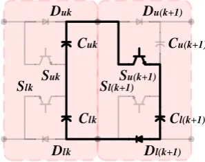
2. 1. Proposed Module Figure 1 shows the basic structure of the proposed SC module for voltage doubling, which includes two capacitors, two switches, and two diodes. The related charging strategy for this module makes the voltage of the (k+1)th module twice as much as the voltage of the kth module. Thus, as shown in Figure 2, each capacitor of the (k+1)th module should be charged by two capacitors of the kth module. For charging upper (lower) capacitors of (k+1)th module, lower (upper) switches of this module have to be turned on.
Figure 1. Proposed SC module for voltage doubling
Figure 2. The charging paths for voltage doubling
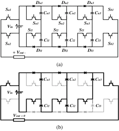
It should be considered that in each module, the voltage of each capacitor cannot drop to less than 50% of the intended voltage. Also, during the charging procedure one switch and one diode of the module is in the path. 2. 2. Operating Principles Figure 3.a shows the configuration of the proposed pulsed power generator for n modules. This structure consists of two half-bridge converters and a few switched capacitors cells in between which are connected together in series. The capacitors’ charging method for the proposed structure is in a way that its current stress is lower than MG structures. Using the input voltage source in forming output pulse is another feature of this topology. Moreover, the switches do not tolerate negative voltage when they are off. As a result, there is no need to use any series diodes along with the switches.
Figure 3.b shows the output voltage pulse of a three-module system in a switching cycle and the switching states of all switches. Note that based on the shape of the required pulse, the order of switching can be rearranged. There are two charging (see Figures 4.b and 4.c) and two discharging states (see Figure 5) which have to be inserted in a switching cycle. In order to show the performance of the proposed structure, a three-module sample is investigated (see Figure 4.a). Figure 4.b shows the upper capacitors charging paths. All upper capacitors are simultaneously charged in a way that the voltage of each capacitor is the sum of two capacitors voltages from the previous module. Similarly, lower capacitors are charged with the equivalent circuit of Figure 4.c.
Dun
Dln Cun
Cln Sun Sln
Duk
D
lkC
ukClk
S
uk SlkDu(k+1)
D
l(k+1)C
u(k+1)Cl(k+1)
S
u(k+1)Sa1
Sa2
Sb1
Sb2
Du1 Du2 Dun
Dl1 Dl2 Dln
Cu1 Cu2 Cun
Cl1 Cl2 Cln
Vin S
un
Sln
Su2
Sl2
Su1
Sl1
+ Vout - Proposed Module
(a)
1st
interval 2nd
interval 3rd
interval 4th
interval 5th
interval
t
1t
2t
3t
4t
5a S
1 1 0 0 0 1
a S
2
0 1 1 1 0
u S
1 0 1 1 0 0
l1
S 1 0 0 0 1
u S
2
0 1 1 0 0
l2
S 1 0 0 0 1
u S
3 0 1 1 0 0
l3
S 1 0 0 0 1
b S
1
1 0 1 0 0
b S
2 0 1 0 1 1
(b)
Figure 3. (a) proposed pulsed power system with n modules
(b) output voltage pulse of a three-module system in a switching cycle and their switching states
(a)
(b)
(c)
Figure 4. (a) a three-stage pulse generator and charging
paths of (b) upper and (c) lower capacitors
(a)
(b)
Figure 5. Discharging paths of the capacitors to achieve (a)
negative (b) positive output pulse
After capacitors are charged, they should be discharged according to the load properties. According to Figure 5.a (5.b), from the sum of upper (lower) capacitors’ voltages, negative (positive) pulse is created with a magnitude of -8Vin (+-8Vin).
3. DISCUSSION
3. 1. Multiplication Limit Increasing the voltage ratings of power electronic elements is the main disadvantage of the proposed multiplier topology. Once the capacitors’ voltage has reached the specified limitation of the elements, voltage doubling should stop and the constant charging mode should be used. Henceforth, the circuit modules of Figure 3 need to be changed into Figure 6.a. In this module, diodes Dui and Dli are replaced with switches. As shown in Figure 6.b, each of the two capacitors in (k+1)th module are simultaneously charged by two capacitors of Kth module.
Sa1
Sa2
Sb1
Sb2
Du1 Du2 Du3
Dl1 Dl2 Dl3
Cu1 Cu2 Cu3
Cl1 Cl2 Cl3
Vin
Su3
Sl3
Su2
Sl2
Su1
Sl1
+ Vout
-Cu1 Cu2 Cu3
Cl1 Cl2 Cl3
Vin
Vout = 0
Cu1 Cu2 Cu3
Cl1 Cl2 Cl3
Vin
Vout = 0
Cu1 Cu2 Cu3
Cl1 Cl2 Cl3
Vin
+ Vout - Max. possible output (negative)
Cu1 Cu2 Cu3
Cl1 Cl2 Cl3
Vin
(a)
(b)
Figure 6. (a) proposed module for constant charging mode
and (b) its capacitors’ charging path
For the applications with low input voltage sources (such as a battery, fuel cells and etc.), multiplication is allowed until peak inverse voltage (PIV) reaches of . It should be considered that x is the ratio between acceptable switch’s voltage and its rated value ( ). This implies that the charging mode (doubling or constant) must be chosen in a way that PIV of the circuit component is kept below a certain percentage of the switches nominal voltage.
3. 2. Determinations of the Capacitances and Output Voltage
3. 2. 1. Calculation of Capacitances As previously mentioned (see Figure 2), the capacitors of (k+1)th module are charged by the ones at kth module. To achieve the desired output voltage, the voltage of each capacitors is assumed to be (1-p) percent of its initial voltage (p is the capacitors’ voltage drop percentage due to parallel charging of the capacitors). Note that capacitors calculation is performed for (1,2,4, …, 2n-1) × V
in charging mode for the worst-case scenario. From the charge conservation law, one can have:
0 0
( ) ( )
total total
q t− =q t+ (1)
The net charge of the system before connection of the capacitors of kth and (k+1)th modules is :
k1
total 0 C k1 0 (k 1)eq C (k 1)eq 0
k1 C k1 0
C
q (t ) ( )2V (t ) C V (t )
2 C V (t )
− − −
− + − +
− −
= + =
(2)
After charging of next module by previous one, the net charge of the system becomes:
1
0 1 0 ( 1) ( 1) 0
( ) ( )2 ( ) ( )
2
k
total C k k eq C k eq
C
q t+ = V− t+ +C + V− + t+ (3)
Considering the capacitor voltage at (k+1)th module as VC k1(t0 ) (1 p V) C k1(t0 )
+ −
− = − − and equalizing Equations
(2) and (3), the following equation can be achieved.
( 1) 1 ( 1)1 1
2(1 ) (1 )
k eq k k k
p p
C C C C
p p
+ = − + = − (4)
Eventually, the equivalent capacitance (Ceq) of the circuit resulted from the serial connection of all the capacitors (as shown in Figure 5.a) is calculated by the following equation:
1
1
1 2 1
1 1 1 1 1 (1 )
...
k n
k
eq u u uk u
p
C C C C C p
−
=
−
= + + + =
(5)In accordance with load properties, during discharging process (time intervals of [t2-t3] and [t4-t5] in Figure 3.b), an α percent voltage drop is occurred for equivalent voltage of series capacitors.
eq
eq
q q
C
V V
= =
(6)
Considering equal discharging intervals for positive and negative pulses (T0=t2-t3=t4-t5), the charge variation of the Ceq during the discharging process can be calculated as:
0
0 0
0 . 0 . . . (1 )
− −
=
=
loadeq = − load eqT t
T T eq R C R C
load eq eq
load
V
q i dt e dt C V e
R (7)
Finally:
0 .ln(1 )
eq load
T C
R
− =
− (8)
Hence, every capacitance in the structure can be calculated using Equations (4)-(8), in a way that demonstrated as follows:
1 1
0
1
(1 )
(1 )
, 1, 2, ,
.ln(1 )
k n k
k k
load
p p
T
p p
C k n
R
− −
=
−
−
−
= =
−
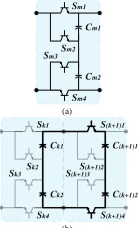
(9)3. 2. 2. Maximum Output Voltage Calculation Figure 7 shows the charging paths of the lower capacitors in different modules considering non-idealities for all circuit components (Figure 4.c with real components). The same process is carried out for the upper capacitors. Considered non-ideal elements are :
SW on
V : Forward voltage of the switch
SW on
R : ON-state resistance of the switch
Cm1
Cm2 Sm2 Sm3
Sm1
Sm4
Ck1
Ck2
Sk2
Sk3
Sk1
Sk4
C(k+1)1
C(k+1)2
S(k+1)2
S(k+1)3
S(k+1)1
S(k+1)4
%
x VratedSW
SW rated
D on
V : Forward voltage of the Diode
D on
R : ON-state resistance of the Diode ESR: Equivalent series resistance of capacitor
The voltage drop of each module can be defined as follows:
( ) ( )
= SW+ SW + D+ D −
on on on on
x V R I V R I ESR I (10)
Considering (1, 2, 4, …, 2n-1)×Vin charging mode, capacitors’ voltages of modules can be written as:
(
)
1 2 1 12( )(1 )
2 2( )(1 ) (1 )
2 ( )(1 ) 2 (1 )
in in
n
k k k k
k in k
V V x p
V V x p x p
V V x p x −= p
= − −
= − − − −
= − − −
−(11)
Maximum output voltage, in this case, can be achieved by calculating the summation of the voltage of the capacitor in all modules as:
(
)
(
1)
max 1
1
2 ( )(1 ) 2 (1 )
n
k
Non Ideal k k m m
out in m
k
V − V x p x −= p
=
=
− − −
− (12)3. 2. 3. Calculation of Maximum Start-up Current High overshoot current is one of the drawbacks of switched capacitor structures such as Marx and other CSVM topologies. In this section, the worst-case scenario is calculated for start-up current and then a switching strategy is presented to reduce the magnitude of this current. Note that the analysis is for a 3-module structure of voltage doubler type.
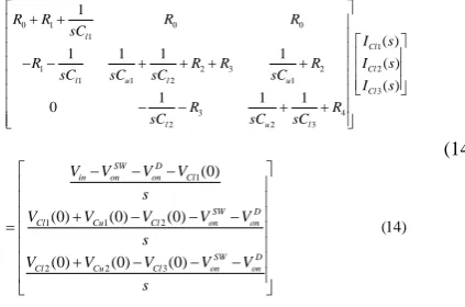
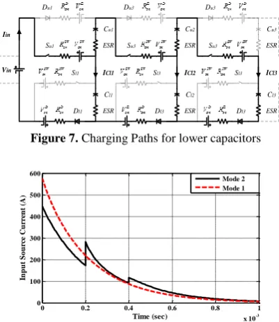
The maximum amount of the input current occurs when the capacitors are totally discharged and their initial charging leads to increasing its current. It is clear that the amount of input current is low during steady state (if the capacitor is not fully discharged). According to Figure 7, input current is calculated as follows:
1 2 3
in Cl Cl Cl
I =I +I +I (13)
Each capacitor’s current can be calculated by solving the following equation.
0 1 0 0
1
1
1 2 3 2 2
1 1 2 1
3
3 4
2 2 3
1
( )
1 1 1 1
( ) ( )
1 1 1
0 + + − − + + + + − − + + l Cl Cl
l u l u
Cl
l u l
R R R R
sC
I s
R R R R I s
sC sC sC sC
I s
R R
sC sC sC
1
1 1 2
2 2 3
(0)
(0) (0) (0)
(14)
(0) (0) (0)
− − − + − − − = + − − − SW D
in on on Cl
SW D
Cl Cu Cl on on
SW D
Cl Cu Cl on on
V V V V
s
V V V V V
s
V V V V V
s (14) In which: 0 1 1 2 1 3 2
4 2 3
= + = = + + = = + + + SW D on on Cl SW D
on on Cu
Cl
SW D
on on Cu Cl
R R R
R ESR
R R R ESR
R ESR
R R R ESR ESR
(15)
With the parameters specified in Table 2 and extracting the values of Equation (15) from semiconductors datasheet, input current can be calculated from the solution of Equation (14).
4602 25418 15511
540. − 33.− 3.−
= t+ t+ t
in
I e e e (16)
Above mentioned calculation is for the simultaneous parallel charging of the capacitors (as shown in Figure 7). It seems that a little delay in capacitors’ charging (maximum for a time constant at each stage) causes reducing the maximum value of input current. After connecting switch Su1, only capacitor Cl1 is charged from the source (0<t< T1). Then, switch Su2 would be connected (T1<t<T2). At this time, in addition to voltage increase of capacitor Cl1, Cl2’s charging begins. Finally, switch Su3 is connected (T2<t). As a result, the input current relation in each stage would be as follows:
4762
1 1
14572
1 2 1 2
4602 25418 15511
1 2 3 2
446. 0
(282.cosh(9953 ) 167.sinh(9953 )). 114. 16.27. 18.339.
− − − − − = = + = + + + = − + t Cl t in Cl Cl
t t t
Cl Cl Cl
I e t T
I I I t t e T t T
I I I e e e T t
(17)
Figure 8 shows the input current of a 3-module system with simultaneous (mode1, Equation (16)) and non-simultaneous charging of the capacitors (mode 2, Equation (17)). It can be seen from this figure that second charging strategy leads to almost 25% reduction of input current. It is worth noting that with both charging modes, the amount of input current is too high. Therefore, following issues has to be considered to avoid high start-up (or any transient state) current.
1) During start-up with fully discharged capacitor, it is necessary to increase the input voltage source gradually to avoid high current spike (it requires variable DC source). Otherwise, limiting resistors (or inductors) during start-up are required to limit the input current. Another option can be initializing the circuit with switching of the switches in linear mode which make the switch as resistor. During start-up or transient, the amount of current reduces to a great extent and after reaching steady state, it returns back to switch mode.
Cu1
ESR
Du1
Dl1 Sl1
Cl1
ESR
Su1
Cu2
ESR
Cl2
ESR
Cu3
ESR
Du3
Dl3 Sl3
Cl3
ESR
Su3
Vin
Du3
Dl3 Sl3 Su3
Iin
ICl1 ICl2 ICl3
Figure 7. Charging Paths for lower capacitors
0 0.2 0.4 0.6 0.8 1
x 10-3
0 100 200 300 400 500 600
Time (sec)
In
p
u
t
S
o
u
rc
e
C
u
rr
en
t
(A
)
Mode 2 Mode 1
Figure 8. Start-up current for the case with fully discharged
capacitors with simultaneous charging of all capacitors (mode 1) and non-simultaneous charging of the capacitors (mode 2)
3. 3. Comparison Study By examining the pros and cons of the basic structures, it is evident that the best structure is the one which has better evaluation indicators than the others. These indicators are divided into two groups of power circuit and control circuit. The number of power semiconductor devices, the number of capacitors, and the Total Standing Voltage (TSV) are among the most important indicators of power circuit assessment. Because the driver circuits have a significant effect on the volume, weight, complexity, and cost of the final circuit, the number of the driver circuits is considered as one of the most important indicators among the control parameters. Table 1 shows different comparison parameters based on input and output voltages ratios in topologies. Two types of modules, doubling and constant, are proposed to take advantage of the both Marx-based and multiplier circuits at the same time.
All of the comparison indices (except for the number of capacitors) in the constant charging mode are better (or at least similar) than other topologies. The number of capacitors is twice as many as in the other topologies, which is the main drawback of this topology in this mode. However, the number of series diodes is zero which improves the problem. According to Table 1, the proposed doubling topology has better performance for all comparison indices except for the PIV. It means that this topology is appropriate for low-input sources, which were the main focus of this paper. Also these two types of modules have the capability to be combined with each other.
4. SIMULATION AND EXPERIMENTAL RESULTS
In this section, to prove the accurate performance of the designed converter, simulation and experiments are carried out. To examine the performance of the proposed topology, a simulation has been done for a prototype consisting of 5 modules with the charging mode of (1, 2, 4, 4, 4)×Vin. Notice that the first three modules are of the doubling kind and the other two are of the constant voltage kind. Considering this charging mode and by a 100 V input source, a maximum output voltage of 1.6 kV is attained, at the frequency of 200 Hz. In the simulation, the MATLAB software has been used. Figure 9 shows the simulated output pulse, a few selected capacitors voltage of the circuitand current respectively.
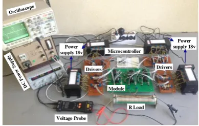
As shown in Figure 10, the laboratory experimental setup has been implemented using both proposed modules combined together and parameters of the Table 2. The IGBTs utilized in the prototype are 15n120 (1200 V) without any series or antiparallel diodes. The switching scheme has been generated by utilizing a AVR ATmega16A. Figure 11 shows the experimental output voltage of the circuit and capacitors voltages of the first three modules. Note that capacitor voltage ripples follow the aforementioned theoretical basis in part B of the section 3.
TABLE 1. Comparison between the Proposed Converter and
Other Marx Topologies (N= )
Items
Proposed (doubling mode)
Proposed (constant mode)
[17] [16] [15]
IGBT 4N 5N 4N 5N
Diodes 0 7N 6N 4N
Driver 4N 5N 4N 5N
Capacitors 2N N N N
TSV
(*Vin) 6N-2 8N 12N 10N 9N
TABLE 2. Simulation and experimental parameters
Items Values
Input voltage 100 V
Output voltage 1.6 kV
C11, C12 1000 µF (150 V)
C21, C22 100 µF (250 V)
C31, C32 10 µF (450 V)
Load 10 KΩ
IGBT 15n120 (1200 V)
Diode RHRP15120 (1200 V)
V out V in −
−
2
2 2log 2N+
2
2 2 log 2N − +
2
2 2log 2N+
2
0.7 0.705 0.71 0.715 0.72 0.725 0.73 -1500
-1000 -500 0 500 1000 1500
Time (sec)
V
o
u
t
0.7 0.705 0.71 0.715 0.72 0.725 0.73
97 98 99 100
V
C
1
2
0.7 0.705 0.71 0.715 0.72 0.725 0.73
-20 0 20
I
C
1
2
0.7 0.705 0.71 0.715 0.72 0.725 0.73
195 195.5 196
V
C
2
2
0.7 0.705 0.71 0.715 0.72 0.725 0.73
-10 0 10
I
C
2
2
0.7 0.705 0.71 0.715 0.72 0.725 0.73
389.5 390 390.5
V
C
3
2
0.7 0.705 0.71 0.715 0.72 0.725 0.73
-10 0 10
I
C
3
2
Figure 9. Simulation results: Output voltage, capacitors
voltage and currents for different modules
Figure 10. A laboratory test setup
Figure 11. Experimental waveforms for output voltage,
upper capacitors voltage at modules 1,2 and 3 (Vcu1, Vcu2, Vcu3) (Differential Probes are set at × 500 for CH3 and × 200 for CH1, CH2 and CH4. The internal probe of the oscilloscope is set at × 100.)
5. CONCLUSION
This paper proposed a modular SC structure for generating a bipolar high voltage pulsed power. Due to its boosting capability, the presented structure can be an appropriate replacement of Marx structures in applications with low input voltage sources. Two different modules are investigated for the proposed topology with voltage doubling and constant voltage capabilities. The doubling charging mode is used whenever the low input voltage is needed to be boosted with high gain till the rated value of the switches permits. Afterwards, a constant charging mode is applied. The theoretical foundation of the topology and the practical results of the simulation prove that the proposed topology has the capability to produce bipolar combined wide and narrow pulses.
6. ACKNOWLEDGEMENTS
The authors acknowledged the funding support of Babol Noshirvani University of Technology through grant program No. BNUT/ 389051 /97.
7. REFERENCES
1. Akiyama, M., Sakugawa, T., Hosseini, S., Shiraishi, E., Kiyan, T., Akiyama, H.:, ‘High-Performance Pulsed-Power Generator Controlled by FPGA’, IEEE Transactions on Plasma Science, 2010, Vol. 38, No. 10, 2588-2592.
2. Hidenori, A., Takashi, S., Takao, N., Koichi, T., Naoyuki, S., “Industrial applications of pulsed power technology”, IEEE Microcontroller
Voltage Probe
R Load Module
Drivers Drivers
Power supply 18v Power
supply 18v
Cu3 V
Cu2 V
Cu1 V
Transactions on Dielectrics and Electrical Insulation, Vol. 14, No. 5, (2007), 1051-1064.
3. Akiyama, H., Sakai, S., Sakugawa, T., Namihira, T., “Environmental applications of repetitive pulsed power”, IEEE Transactions on Dielectrics and Electrical Insulation, Vol. 14, No. 4, (2007), 825-833.
4. Wu, Y., Liu, K., Qiu, J., Liu, X., Xiao, H., “Repetitive and high voltage Marx generator using solid-state devices”, IEEE Transactions on Dielectrics and Electrical Insulation, Vol. 14, No. 4, (2007), 937-940.
5. Choi, JG., “Introduction of the magnetic pulse compressor (MPC)-Fundamental review and practical application”, Journal of Electrical Engineering and Technology, Vol. 5, (2010), 484-492.
6. Roark, R., Parten, M., Masten, L., Burkes, T., “Pulse-forming networks with time-varying or nonlinear resistive loads”, IEEE Transactions on Electron Devices, Vol. 26, No. 10, (1979), 1541-1544.
7. Guillemin, E., “Synthesis of Passive Networks”, John Wiley, New York, (1957).
8. Zabihi, S., Zare, F., Ledwich, G., Ghosh, A., Akiyama, H., “A new pulsed power supply topology based on positive buck-boost converters concept”, IEEE Transactions on Dielectrics and Electrical Insulation, Vol. 17, No. 6, (2010), 1901 -1911. 9. Elserougi, A., Ahmed, S., Massoud, A., “A boost converter-based
ringing circuit with high-voltage gain for unipolar pulse generation”, IEEE Transactions on Dielectrics and Electrical Insulation, Vol. 23, No. 4, (2016), 2088-2094.
10. Elserougi, A., Massoud, AM., Ahmed, S., “A Boost-Inverter-Based Bipolar High-Voltage Pulse Generator”, IEEE Transactions on Power Electronics, Vol. 32, No. 4, (2017), 2846-2855.
11. Kim, JH., Lee, SC., Lee, BK., Shenderey, S., Kim, JS., Rim, GH., “A high-voltage bi-polar pulse generator a using push-pull inverter”, IECON, (2003), 102-106.
12. Wu, TF., Tseng, S., Wu, MW., Chen, YM., “Narrow pulsed voltage generator for liquid food sterilization”, 21th Applied Power Electronics Conference and Exposition, (2006), 1354-1360.
13. Kang, B., Low, KS., Soon, JJ., Tran, QV., “Single-Switch Quasi-Resonant DC–DC Converter for a Pulsed Plasma Thruster of Satellites”, IEEE Transactions on Power Electronics, Vol. 32, No. 6, (2017), 4503-4513.
14. Elserougi, AA., Faiter, M., Massoud, AM., Ahmed, S., “A Transformerless Bipolar/Unipolar High-Voltage Pulse Generator With Low-Voltage Components for Water Treatment Applications”, IEEE Transactions on Industry Applications, Vol. 53, No. 3, (2017), 2307-2319.
15. Sakamoto, T., Nami, A., Akiyama, M., Akiyama, H., “A repetitive solid state Marx-type pulsed power generator using multistage switch-capacitor cells”, IEEE Transactions on Plasma Science, Vol. 40, No. 10, (2012), 2316-2321.
16. Canacsinh, H., Redondo, L., Silva, JF., “Marx-type solid-state bipolar modulator topologies: Performance comparison”, IEEE Transactions on Plasma Science, Vol. 40, No. 10, (2012), 2603-2610.
17. Redondo, L., Canacsinh, H., Silva, JF., “Generalized solid-state marx modulator topology”, IEEE Transactions on Dielectrics and Electrical Insulation, Vol. 16, No. 4, (2009), 1037-1042. 18. Redondo, L., “A DC voltage-multiplier circuit working as a
high-voltage pulse generator”, IEEE Transactions on Plasma Science, Vol. 38, No. 10, (2010), 2725-2729.
19. Elserougi, AA., Abdelsalam, I., Massoud, AM., Ahmed, S., “A full-bridge submodule-based modular unipolar/bipolar high-voltage pulse generator with sequential charging of capacitors”, IEEE Transactions on Plasma Science, Vol. 45, No. 1, (2017), 91-99.
A High Gain Bipolar Pulse Generator with Low Voltage Input Source
H. Gholamalitabara, J. Adabia, M. Rezanejadb
a Department of Electrical and Computer Engineering,Babol Noshirvani University of Technology, Babol, Iran b Department of Electrical and Computer Engineering, University of Mazandaran, Babolsar, Iran
P A P E R I N F O
Paper history: Received 30 May 2019
Received in revised form 21 July 2019 Accepted 28 July 2019
Keywords:
Bipolar Pulsed Power Generator Switched-Capacitor
Modular Marx Generator
هدیکچ
عون یداهنشیپ لوژام رد .تسا هدش یفرعم یسلاپ ناوت عبانم دیلوت تهج هدنیازفا ینزاخ چییوس لوژام عون ود ،هلاقم نیا رد
یجورخ ژاتلو ،لوا دنربارب مه اب یجورخ ژاتلو و یدورو ژاتلو ،مود عون لوژام رد و تسا ربارب ود یدورو ژاتلو هب تبسن
لوژام نیا نداد رارق مه رانک اب ،تیاهن رد و یم لصاح رظن دروم ییاهن ژاتلو ،اه
.ددرگ نیا رب هولاع رلاوژام راتخاس هک
یمن هدافتسا رابرس چییوس زا یداهنشیپ یرج سرتسا ،دنک
همین رصانع و عبنم یور رب رتمک ینا ناونع هب نآ هب کیدزن یداه
یم بوسحم راتخاس نیا تیزم مشچ روط هب زین یرادم رصانع دادعت ،نینچمه .دوش
یاقم رد یریگ سکرام راتخاس اب هس
هتفای شهاک .تسا هدش لرتنک رادم یگدیچیپ و هدش مامت هنیزه شهاک هب رجنم هک
نزاخ تابساحم ،همادا رد نایب
هدش و
هیبش و یهاگشیامزآ تست .دیدرگ ماجنا هلوژام جنپ هنومن کی یور رب یداهنشیپ راتخاس ییآراک دییات روظنم هب یزاس
doi: 10.5829/ije.2019.32.08b.08