w w w . i j m r e t . o r g I S S N : 2 4 5 6 - 5 6 2 8 Page 5
Optimization of the thickness of Absorber and
Zinc Oxide Buffer layers of CIGS solar cell
using SCAPS-1D
1*
M A. Hayat,
1G. Babaji,
2Mansur Said,and
3A.B. Ahmed
1
Department of Physics Bayero University Kano Nigeria 2
Department of Physics Yusuf Maitama Sule University Kano Nigeria 3
Department of Physics Gombe State University Gombe Nigeria
Abstract: Advancement in the technology forces the science community to expand in the search of energy.
Solar energy was proven to be the answer for the problem. Solar Cell Capacitance Simulator (SCAPS) is a code used for studying one dimensional properties of a solar cell. Interest in the study of ZnO properties raised as a result of its capability to substitute the toxic CdS. The thickness of both Absorber and Buffer layers were optimized. It was found that the optimized thicknesses of both the Absorber and buffer layers were found to be 2.25µm and 0.02µm respectively. Also from the optimized materials, the Voc, Jsc, FF and efficiency were found to be 0.9426V, 37.944556mA/cm2, 85.29% and 30.51% respectively. The result shows promising outcome of the replacement of CdS and also in good agreement with literature.
Keyword: Solar cell, Absorber & Buffer layers, Voc, Jsc, FF and Efficiency
I. INTRODUCTION
The energy demand is increasing globally,and with the fast depleting fossil fuel source and ever-rising environmental pollution causing problems like global warming, the use of alternate energy has become much more important than any time in history (Das and Kumar, 2018). As the world struggles to address climatic changes, renewable energy is becoming an increasingly important source of electricity.Solar energy is the most available energy source available on earth. Though technologies for converting sunlight energy to power have made a lot of progress, high capital price and low conversion proficiency are the main obstacles to the common use of this technology (Ali and Hossain, 2015).
Thin-film solar cells are introduced and developed as the second generation of solar cells to provide high production capacity at lower energy and material consumption (Poortmans and Arkhipov, 2006). Main motivations for the growth of thin-film photovoltaic PV are their potential for high-speed and high-throughput manufacturing and minimum
material requirements that lead to cost reduction. (Arnulf, 2011).
Copper Indium Gallium Di Selenide (CIGS) is one of the most promising materials for thin-film photovoltaic devices because of its appropriate band gap and high absorption
coefficient for solar radiation (Green et al., 2003).
CIGS material is important for terrestrial
applications because of their high efficiency, long-term stable performance, and potential for low-cost
production. Thin-film solar-cells with
polycrystalline Cu(In,Ga)Se2 (CIGS ) absorber layers provide a good alternative to wafer-based crystalline silicon solar cells, which currently constitute the major share of photovoltaics installed and used worldwide.(Kessler and Rudmann, 2004).
w w w . i j m r e t . o r g I S S N : 2 4 5 6 - 5 6 2 8 Page 6
II. THEORETICAL BACKGROUND
The parameters used to characterize the output of solar cells for given irradiance and
temperature are short circuit current (Isc), short
circuit current density (Jsc), open-circuit voltage
(Voc), maximum power point (Pmax), current at
maximum power point (Imax), voltage at maximum
power point (Vmax), fill factor (FF), conversion
efficiency (ŋ), series resistance (Rs), and shunt
resistance (Rsh) and can be obtained from I-V
characteristic measurement.
The short circuit current (Isc) is the current
through the solar cell when the voltage across the
solar cell is zero. The open-circuit voltage (Voc) is
the voltage across the solar cell when the current through the solar cell is zero. The maximum power
point (Pmax) is the condition under which the solar
cell generates its maximum power; the current and
voltage are defined as Imaxand Vmax, respectively.
The fill factor (FF) is defined as the ratio of Pmax
divided by the product of Vocand Isc. The conversion
efficiency is defined as the ratio of Pmax to the
product of the input light irradiance (E) and the surface area of the solar cell (A).
𝐼 = 𝐼𝑜 1 − 𝑒
𝑞𝑉
𝐾𝑇 + 𝐼𝐿 (1)
𝑉𝑜𝑐 =𝐾𝑇𝑞 𝐼𝑛𝐼𝐼𝑠𝑐
0 (2)
𝐹𝐹 = 𝑃𝑚𝑎𝑥
𝑉𝑜𝑐×𝐼𝑠𝑐 =
𝑉𝑚𝑎𝑥×𝐼𝑚𝑎𝑥
𝑉𝑜𝑐×𝐼𝑠𝑐 (3)
ŋ=𝑃𝑚𝑎𝑥
𝑃𝑖𝑛 =
𝑉𝑚𝑎𝑥×𝐼𝑚𝑎𝑥
𝐸×𝐴 =
𝑉𝑜𝑐×𝐼𝑠𝑐×𝐹𝐹
𝐸×𝐴 (4)
2.1. Governing equations of SCAPS
SCAPS-1D version 3.3.06 is a one-dimensional solar cell device simulator, developed at Electronics and Information Systems (ELIS), University of Gent, Belgium. SCAPS is freely available to the PV research community. The user can describe a solar cell as a stack of up to seven layers with different properties, such as thickness, optical absorption, doping, defect densities, and defect distribution. It is then pissible to simulate a
number of common measurements: I-V, C-V, C-f, QE (Mandadapuet al., 2017).
SCAPS is capable of solving the basic semiconductor equations, the Poisson equation and the continuity equations for electrons and holes:
𝑑2
𝑑𝑥2Ѱ 𝑥 =
𝑒
𝜀0𝜀𝑟 𝑝 𝑥 − 𝑛 𝑥 + 𝑁𝐷− 𝑁𝐴+ 𝜌𝑃− 𝜌𝑛 (5)
Where Ѱ is electrostatic potential, e is an electrical charge, εr is relative, and ε0 is the vacuum permittivity, p and
n are hole and electron concentrations, ND is charged impurities of donor and NA is acceptor type, ρp, and ρn are
holes and electrons distribution, respectively. The continuity equations for electrons and holes are:
𝑑𝑗𝑛
𝑑𝑥 = 𝐺 − 𝑅 (6)
𝑑𝑗𝑝
𝑑𝑥 = 𝐺 − 𝑅 (7)
where, 𝑗𝑛=Electron Current Density, 𝑗𝑝=Hole Current Density, G=Recombination Rate, R= Generation Rate.
Carrier transport in semiconductors occurs by drift and diffusion and can be expressed by the equations:
𝐽𝑛 = 𝐷𝑛𝑑𝑑𝑥𝑛 + 𝜇𝑛𝑛𝑑∅𝑑𝑥 (8) 𝐽𝑝= 𝐷𝑝
𝑑𝑝 𝑑𝑥+ 𝜇𝑝𝑝
𝑑∅
𝑑𝑥 (9)
SCAPS calculates the solution of the basic semi-conductor equations in one dimension and in
steady-state conditions (Ouedraogoet al., 2013).
w w w . i j m r e t . o r g I S S N : 2 4 5 6 - 5 6 2 8 Page 7 Table 1: The parameters for the CIGS-based solar cell at 300K.
Parameters CIGS[Mostefaouni et al,2015]
nZnO:Al [Oubda
et al,2015]
ZnO [Asaduzzaman
et al,2017]
Eg(eV) 1.5 3.3 3.3
𝜺𝒓 13.6 9 10
𝝌(𝒆𝑽) 4.5 4.65 4.6
µn(cm2V-1s -1
)
100 100 100
µp(cm2V-1s -1
)
25 25 30
NC(cm-3) 2.2e18 2.2e18 1.5e18
NV(cm-3) 1.8e19 1.8e19 1.8e19
Vt(cm/s) 1e7 1e7 1e7
Vt(cm/s) 1e7 1e7 1e7
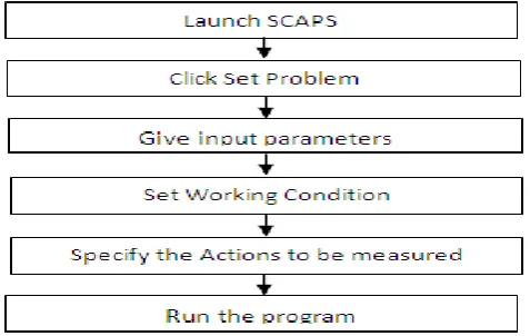
III. Procedure
Figure 1 explains the simulation process.
Figure 1. SCAPS working procedure
SCAPS has been designed to simulate CIGS and CdTe-based thin-film solar cell devices. The user can calculate results in the form of following characteristics: I-V, C-V, C-f, Q(λ), band diagrams, electric field, carrier densities, partial recombination currents. The user can set parameters of materials and an operating point: temperature, voltage, and frequency and illumination condition. The device is represented as a stack of layers, up to 7 semiconductor layers with specified properties, separate entries for interface parameters and two additional layers for front and back contacts. All layers are characterized by the numerical description of parameters (Burgelman et al., 2016)
A typical CIGS-based solar cell structure consists of a p-type wide-bandgap absorber layer,a back contact glass substrate. An n-type buffer layer made of and window layer made of n-ZnO:Al
w w w . i j m r e t . o r g I S S N : 2 4 5 6 - 5 6 2 8 Page 8 layer has its own special electrical and optical properties, which should be specified inside the SCAPS software as inputs before executing. The electro-optical properties of materials used for the specific layers are extracted from known and reliable numerical models and experimental studies.
The simulations are conducted by specifying the materiel parameters in each defined layer of the device structures as the input parameters. Within the reasonable ranges, the material parameters selected from the reported literature for all the layers are shown in Table 1. In order to study the effects of thickness on the performances of the CIGS solar cells, we have proceeded layer by layer in such a way that the thickness of two layers are kept unchanged and those of the third layer are varied. This has allowed us to attain solar cells with high efficiencies. The J-V characteristic was simulated with the AM1.5 illumination conditions (100mW/cm2). The simulation started by changing the thickness of the absorber layer from 1 to 5μm, and the thickness buffer layer was changed from 0.01µm to 0.10µm, and the variation of the cell performance has been reviewed. The
open-circuit voltage (Voc), short circuit current density (Jsc), fill factor (FF), efficiency (η) is calculated by the
software.
IV. RESULTS AND DISCUSSION
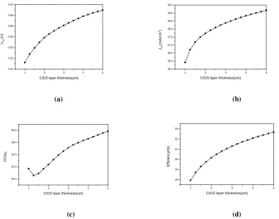
4.1 Effect of Absorber Layer Thickness with ZnO as Buffer Layer
(a) (b)
(c) (d)
Figure 2. Variation of (a) Voc (b) Jsc (c) FF and (d) Efficiency as a function of CIGS layer thickness.
The simulation results show that the general performance of the cell increases while the thickness of the absorber layer is increased. The entire measured parameters, including Voc, Jsc, the Fill factor (FF%) and efficiency almost follow the same pattern. Figure 2 shows the variation of the cell performance due to the absorber thickness changes. The photovoltaic cell parameters for various thicknesses of CIGS, ranging from 1 to 5µm are shown in Figure 2. It was observed that as the thickness of CIGS is increased both Voc and Jsc of CIGS solar cells are increased as well. In fact, this allows the collection of lightening wavelengths, which contribute to the generation of the electron-hole pairs (Chelvanathan et al., 2010) and results in the increase of
1 2 3 4 5
0.91 0.92 0.93 0.94 0.95 0.96 0.97
VOC
(V
)
CIGS layer thickness(um)
1 2 3 4 5
35.5 36.0 36.5 37.0 37.5 38.0 38.5 39.0 39.5
JSC
(m
A
/cm
2)
CIGS layer thickness(um)
1 2 3 4 5
84.5 85.0 85.5 86.0 86.5
F
F
(%
)
CIGS layer thickness(um)
1 2 3 4 5
28 29 30 31 32 33
E
ff
ic
ie
ncy
(%
)
w w w . i j m r e t . o r g I S S N : 2 4 5 6 - 5 6 2 8 Page 9 the Voc and Jsc. It is generally agreed that the values of Voc and Jsc will be reduced if the thickness of the absorber layer is reduced. This may be caused by the recombination process at the back contact of the solar cell. Figure 2d shows the variation of the electric efficiency versus the thickness of the CIGS absorber layer,but over
2.25μm, the efficiency variation seems to be very slow. The efficiencies was recorded as 30.49%. Note that as
the thickness of CIGS increases the efficiency increases monotonically. On the other hand, the fill factor of the solar cell increases as well with the increase of the thickness of the absorber layer. This is in good agreement with the previous results reported by Heriche et al., 2016 and Chelvanathan et al., 2010.
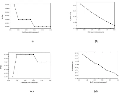
4.2 Effect of Buffer Layer (ZnO) Thickness
(a) (b)
(c) (d)
Figure 3. Variation of (a) Voc (b) Jsc (c) FF and (d) Efficiency as a function of CIGS layer thickness.
From Figure 3, it was found that the open-circuit voltage of device decreases with the increase of the buffer layer thickness, but the short circuit current density decreases considerably, particularly for larger thickness. The efficiency decreases monotonically with the increase of buffer layer thickness, as shown in Figure 3c. The larger the thickness of the buffer layer, the higher the number of absorbed photons that transport energy in the layer. This results in the loss of these photons leading to the decrease of the number of photons reaching the absorber layer.the optimum thickness was found to be 0.02µm.
V. Conclusion
The cell performance was simulated and analyzed by the function of the buffer layer and absorber layer thickness. The optimum thickness of CIGS absorber layer and ZnObuffer of a CIGS thin film solar cell were found to be 2.25µm and 0.02µm respectively. There is a compromise between having a thin and a minimum recombination current density in these layer thickness. Although these results can help us to fabricate a desired CIGS thin film solar cell, there are some other effective parameters which
0.00 0.02 0.04 0.06 0.08 0.10
0.91590 0.91595 0.91600 0.91605 0.91610 0.91615 0.91620
VOC
(V
)
ZnO layer thickness(um)
0.00 0.02 0.04 0.06 0.08 0.10
35.75 35.80 35.85 35.90 35.95
JSC
(m
A
/cm
2)
ZnO layer thickness(um)
0.00 0.02 0.04 0.06 0.08 0.10
84.890 84.895 84.900 84.905 84.910 84.915 84.920
F
F
(%
)
ZnO layer thickness(um)
0.00 0.02 0.04 0.06 0.08 0.10
27.80 27.82 27.84 27.86 27.88 27.90 27.92 27.94 27.96 27.98
E
ff
iciency
(%
)
w w w . i j m r e t . o r g I S S N : 2 4 5 6 - 5 6 2 8 Page 10 can affect the cell performance and need to be
investigated in further studies.
Reference
[1.] Arnulf, J.W. (2011). Progress in chalcopyrite
compound semiconductor research for
photovoltaic applications and transfer of results into actual solar cell production, Solar Energy Materials and Solar Cells, vol. 95, pp.1509 –1517.
[2.] Asaduzzaman, Md., Billal, H., Karamot, A.,
and Bahar, A.N. (2017).Non-Toxic Buffer Layers in Flexible Cu(In,Ga)Se2 Photovoltaic Cell Applications with Optimized Absorber
Thickness,International Journal of
Photoenergy.
https://doi.org/10.1155/2017/4561208
[3.] Burgelman, M., Decock, K., Niemegeers, A.,
Verschraegen, J., and Degrave, S. (2016). SCAPS manual version 3.3.06, Department of ELIS, University of Gent, Belgium, pp 1-110.
[4.] Chelvanathan, P., Hossain, M. I., Amin, N.
Performance analysis of copper-indium
gallium diselenide (CIGS) solar cells with various buffer layers by SCAPS, Current Appl. Phys.10 (2010) S387-S391.
[5.] Das, B., andKumar, A.(2018). “An NLP
approach to optimally size an energy storage system for proper utilization of renewable energy sources proper utilization of renewable energy sources,” Procedia Computer Science., vol. 125, pp. 483–491.
[6.] Green M. A., Emery K., King D. L., Igari S.,
and Warta W. (2003). “Solar cell efficiency
tables (Version 22),” Progress in
Photovoltaics: Research and Applications, vol. 11, no. 5, pp. 347–352.
[7.] Heriche, H., Rouabah, Z., and Bouarissa, N.
(2016). High-efficiency CIGS Solar Cells with optimization of layers thickness and doping. Optik-International Journal for light and
electron optics. Doi
http://dx.doi.org/doi:10.1016/j.ijleo.2016.09.0 71.
[8.] Kazmerski L.L. (2016). Best research solar
cell efficiencies. Available
http//www.nrel.gov/
ncpv/images/efficiency_chart.jpg
[9.] Kessler F. and RudmannD., "Technological
aspects of flexible CIGS solar cells and
modules," Solar Energy, vol. 77, pp. 685-695, 2004.
[10.]Mostefaoui, M. Mazari, H. Khelfi, S.
Bouraiou, A., and Dabou, R. (2015). Simulation of High-Efficiency CIGS solar cells with SCAPS-1D software. International conference on technology and materials for renewable energy, Energy procedia 74, pp. 736-744.
[11.]Oubda, D., Kebre, M.B., Zougmore, F.,
Njomo, D., and Ouattara, F. (2015). Numerical
simulation of Cu(In,Ga)Se2 Solar cells
performances. Journal of Energy and Power Engineering. 9, pp. 1047-1055.
[12.]Ouedraogo, S., Zougmore, F., and Ndjaka,
J.M. (2013). Numerical Analysis of Copper-Indium-Gallium-Diselenide-Based Solar Cells by SCAPS-1D. International Journal of Photoenergy, 2 pp 1-9.
[13.]Poortmans, J. and Arkhipov, V. (2006),