Selecting Best Feeding Technique of a Rectangular
Patch Antenna for an Application
Charles U. Ndujiuba1,*, Adetokunbo O. Oloyede2
1Electrical & Information Engineering, Covenant University, Ota, Nigeria 2Computer Engineering Department, College of Technology, Yaba Lagos, Nigeria
Abstract
This work analyses the performance of different feeding techniques for rectangular microstrip patch antennas used in wireless communications applications, such as in Wimax and LTE technologies. Three types of feeding arrangements are discussed here; Microstrip Line feed, Coaxial probe feed, and Aperture-coupled feed techniques. The performance of microstrip patch antenna system depends on the characteristics of the antenna element and the substrate as well as the feed configuration employed. Here the principal characteristics of interest are the antenna input impedance, mutual coupling, bandwidth, radiation pattern and return loss. In this paper, we analyze these characteristics for each feed technique, and compare them with those of the other techniques. This enables the system designer to make well informed judgement on the best feeding arrangement for his application. MATLAB has been used for the simulations and evaluations of the various performance metrics.Keywords
Return Loss, LTE systems, Antenna array, Mutual coupling, Input impedance, Bandwidth, Radiation pattern, MIMO1. Introduction
The Microstrip patch antennas are well known for their performance and their robust design, fabrication and their extent of usage. The usage of the Microstrip antennas is spreading widely in all the fields and areas and now they are booming in the commercial aspects due to their low cost of the substrate material and the fabrication. It is also expected that due to the increasing usage of the patch antennas in the wide range this could take over the usage of the conventional antennas for the maximum applications [4]. Microstrip patch antenna has several applications, some of which are discussed below:
1.1. Mobile and Satellite Communication Application
Mobile communication requires small, low-cost, low profile antennas. Microstrip patch antenna meets all requirements and various types of microstrip antennas have been designed for use in mobile communication systems. In case of satellite communication circularly polarized radiation patterns are required and this can be realized using either square or circular patch with one or two feed points.
1.2. Global Positioning System Applications
Nowadays microstrip patch antennas with substrate
* Corresponding author:
[email protected] (Charles U. Ndujiuba) Published online at http://journal.sapub.org/ijea
Copyright © 2015 Scientific & Academic Publishing. All Rights Reserved
having high permittivity materials are used for global positioning system. These antennas are circularly polarized, very compact and quite expensive due to its positioning. It is expected that millions of GPS receivers will be used by the general population for land vehicles, aircraft and maritime vessels to find their position accurately.
1.3. Radio Frequency Identification (RFID)
RFID uses in different areas like mobile communication, logistics, manufacturing, transportation and health care [2]. RFID system generally uses frequencies between 30 Hz and 5.8 GHz depending on its applications. Basically RFID system is a tag or transponder and a transceiver or reader.
1.4. Worldwide Interoperability for Microwave Access (WiMax)
The IEEE 802.16 standard is known as WiMax. It can reach up to 30 mile radius theoretically and data rate 70 Mbps. Microstrip patch antenna generates three resonant modes at 2.7, 3.3 and 5.3 GHz and can, therefore, be used in WiMax compliant communication equipment.
1.5. Radar Application
1.6. Rectenna Application
Rectenna is a rectifying antenna, a special type of antenna that is used to directly convert microwave energy into DC power. Rectenna is a combination of four subsystems i.e. Antenna, ore rectification filter, rectifier, post rectification filter. In rectenna application, it is necessary to design antennas with very high directive characteristics to meet the demands of long-distance links. Since the aim is to use the rectenna to transfer DC power through wireless links for a long distance, this can only be accomplished by increasing the electrical size of the antenna [15].
1.7. Telemedicine Application
In telemedicine application antenna is operating at 2.45 GHz. Wearable microstrip antenna is suitable for Wireless Body Area Network (WBAN). The proposed antenna achieved a higher gain and front to back ratio compared to the other antennas, in addition to the semi directional radiation pattern which is preferred over the omni-directional pattern to overcome unnecessary radiation to the user's body and satisfies the requirement for on-body and off-body applications. A antenna having gain of 6.7 dB and a F/B ratio of 11.7 dB and resonates at 2.45GHz is suitable for telemedicine applications.
1.8. Medicinal Applications of Patch
It is found that in the treatment of malignant tumours the microwave energy is said to be the most effective way of inducing hyperthermia. The design of the particular radiator which is to be used for this purpose should possess light weight, easy in handling and to be rugged. Only the patch radiator fulfils these requirements. The initial designs for the Microstrip radiator for inducing hyperthermia was based on the printed dipoles and annular rings which were designed on S-band. And later on the design was based on the circular microstrip disk at L-band. There is a simple operation that goes on with the instrument; two coupled Microstrip lines are separated with a flexible separation which is used to measure the temperature inside the human body.
The most preferred antennas on any mobile unit for a Multiple-Input-Multiple-Output (MIMO) system are microstrip or patch antennas, due to their low cost and ease of fabrication. These benefits justify our interest in this
subject.
The main drawback of these antennas is low bandwidth and there are various techniques proposed for improving the bandwidth.
The bandwidth of the microstrip patch antenna can be improved by increasing the thickness of substrate or by decreasing its electric permittivity value.
In addition to compatibility with integrated circuit technology, microstrip antenna systems offer other benefits such as thin profile, light weight, low cost and conformability to a shaped surface. Its main disadvantage is inherent narrow bandwidth arising from the fact that the region under the patch is basically a resonant cavity with a high quality factor.
Feed structures for microstrip antennas take various forms. The main ones are the coaxial probe, the microstripline, and the aperture coupling methods.
The choice of the feed arrangement may depend on the application of the antenna system. For example, at millimeter wave frequencies the use of the aperture coupling obviates problems of large probe self-reactances associated with probe feeds. The connector effects, at the junction of the probe and the antenna element, give rise to fundamental limits to antenna performance due to radiation from the discontinuity at the junction.
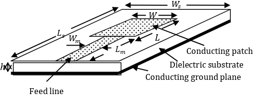
In the microstrip line feed technique, a conducting strip is connected directly to the edge of the Microstrip patch. The conducting strip is smaller in width as compared to the patch. This kind of feed arrangement has the advantage that the feed can be etched on the same substrate to provide a planar structure. However, an increase in the thickness of thedielectic substrate will increase surface waves and spurious feed radiation, which hampers the bandwidth of the antenna. This feed radiation also leads to undesired cross polarized radiation. This method is advantageous due to its simple planar structure.
The coaxial feed or probe feed is a very common technique used for feeding Microstrip patch antennas. The inner conductor of the coaxial connector extends through the dielectric and is soldered to the radiating patch, while the outer conductor is connected to the ground plane. The main advantage of this type of feeding scheme is that the feed can be placed at any desired location inside the patch in order to match with its input impedance.
Figure 1. Microstrip line feed techniqu
Feed line 𝐿𝐿𝑠𝑠
𝑊𝑊𝑠𝑠
𝑊𝑊𝑚𝑚
𝐿𝐿𝑚𝑚
ℎ
𝐿𝐿
𝑊𝑊
Conducting ground plane Dielectric substrate
Figure 2. Coaxial probe feed technique
However, its major drawback is that it provides narrow bandwidth of 2-5% and is difficult to model since a hole has to be drilled in the substrate and the connector protrudes outside the ground plane, thus not making it completely planar for thick substrates. Also, for thicker substrates the increased probe length makes the input impedence more inductive leading to matching problems. The microstrip line feed and the coaxial feed suffer from numerous disadvantages.
Figure 3. Aperture-coupled feed technique
The basic geometry of a single aperture-coupled microstrip patch antenna is shown in Figure 3 [1, 2]. It consists of two substrates bonded together and separated by a ground plane between them. On the top substrate is printed the radiating patch (antenna) while a microstrip feedline is printed on the bottom substrate, which is electromagnetically coupled to the patch by means of a small resonant aperture in the ground plane.
Several advantages are obtained by the use of such two-sided configuration. These include isolation of the feed network from the radiating aperture, which eliminates the spurious feed network radiation that can degrade polarization and sidelobe levels. Also, the two-sided configuration provides two distinct microstrip line media so that the antenna substrate can be chosen to optimize the performance of the radiating patches (e.g. low permittivity to improve radiation and increase bandwidth), and the feed substrate can
be chosen independently to optimize feed performance.
2. Analysis of the Performance
Parameters
In general, there are two lines of approach to deduce the radiation fields. One is to find the current distributions along the antenna structure and then obtain the radiation fields from these current sources. The other is to find the fields at the exit region. These fields act as equivalent sources, from which the radiation fields are obtained. Under these two approaches a number of methods of analysis are in use. They can be broadly classified under two categories:
i. Simplified Method
● Transmission-line model
● The Cavity model
● Method of segmentation ii. Exact or Rigorous Method
● The Integral Equation method
In this work the Transmission-Line Model is employed in order to have a fast and efficient procedure for computing the parameters of the radiating patch.
2.1. Transmission-Line Analysis of Patch Antennas
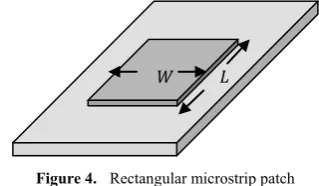
In this model, a rectangular microstrip antenna patch, of figure 3, is viewed as a resonant section of a microstrip transmission line, since it has a physical structure derived from microstrip transmission. The transmission line model does not include surface waves. Therefore, the application is limited to antenna configurations where the thickness and the substrate permittivity are sufficiently small to avoid considerable excitation of those surface waves. But in practice, this is not a severe limitation.
The patch is characterised by the resonant length L (resonant for the fundamental mode), the width W, and
conductivity σp, while the substrate is electrically
characterised by a relative permittivity εr, and a loss tangent δs. Also for the purpose of the analysis the dielectric
substrate is supposed to have infinite dimensions in the plane of the patch, but in practice, it has a length Ls, and a width Ws,
and a thickness h.
Figure 4. Rectangular microstrip patch
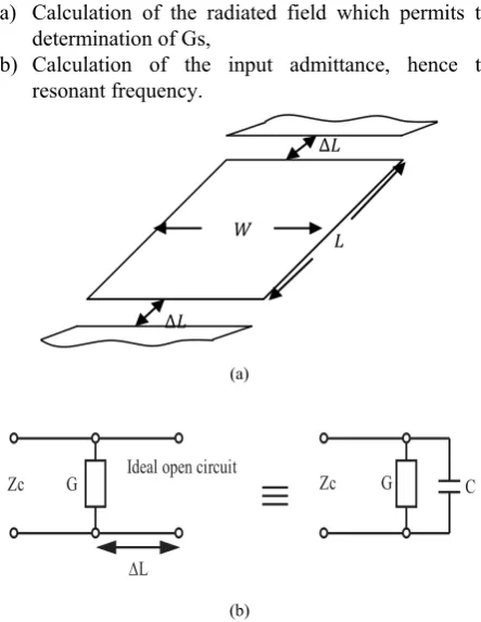
The main step in the modelling of the microstrip antenna by the transmission-line equivalent is the representation of the open-ended terminations by a parallel admittance Ys. These open-ends do not perform as perfect open circuits (Figure 4), because the field lines do not stop abruptly at the
𝐿𝐿 𝑊𝑊
y
x z
Wp Lp
Radiating Patch
Patch Substrate Coupling Aperture
Feed Substrate
Microstrip Feed line Ground
Plane
Wf d
t
Antenna patch
Substrate
Coaxial cable Central conductor
end of the conductor. This extension of stray fields beyond the ends of the strip can be interpreted as an electrical
lengthening ΔL of the line which implies an amount of stored
energy.
In the fundamental mode, only the contribution from the two open ends is important. The sources of radiation can be limited to two narrow zones along the two open ends of the patch.
The field in these two narrow zones can be thought of as the field of two rectangular slots in an infinite, perfectly conducting plane.
For the fundamental mode of the microstrip antenna the tangential field in these two slots can be considered to be uniformly distributed. The calculation can then be decomposed into:
a) Calculation of the radiated field which permits the determination of Gs,
b) Calculation of the input admittance, hence the resonant frequency.
(a)
∆L
Ideal open circuit G
Zc Zc G C
(b)
Figure 5. Schematic representation of open-ends of patch 2.2. Calculation of the Radiated Field
The tangential electrical field in the slot apertures can be written as:
𝐸𝐸𝑥𝑥= 𝑉𝑉ℎ𝑜𝑜 (1)
As a result of the presence of image on the slot we find that
𝑀𝑀��⃗ = 2𝐸𝐸�⃗ʌ𝑒𝑒����⃗ = 2𝐸𝐸𝑦𝑦 𝑥𝑥𝑒𝑒���⃗ 𝑥𝑥ʌ 𝑒𝑒����⃗ = 2 𝑦𝑦 𝑉𝑉𝑜𝑜
ℎ 𝑒𝑒���⃗𝑧𝑧 (2)
The uniform distribution of the tangential electric field,
𝐸𝐸𝑥𝑥 on the slots permits us to calculate the far-field, 𝐸𝐸𝑠𝑠, from
each of the slots.
𝐸𝐸𝑥𝑥
����⃗ = −𝑗𝑗𝑗𝑗𝑗𝑗
4𝜋𝜋 ∫
+ℎ2
−ℎ2 ∫ (
+𝑤𝑤2
−𝑤𝑤2 𝑀𝑀��⃗ʌ𝑢𝑢�⃗). 𝑒𝑒−𝑗𝑗𝑗𝑗 𝑢𝑢��⃗.𝑂𝑂𝑁𝑁 ′
��������⃗. 𝑑𝑑𝑥𝑥′𝑑𝑑𝑧𝑧′ (3)
where w = length of the slot h = width of the slot
𝑗𝑗 =𝑒𝑒−𝑗𝑗𝑗𝑗𝑗𝑗𝑗𝑗 , with 𝑗𝑗 = �𝑥𝑥2+ 𝑦𝑦2 + 𝑧𝑧2 (4)
and
𝑢𝑢�⃗ = 𝑠𝑠𝑠𝑠𝑠𝑠𝑠𝑠𝑠𝑠𝑜𝑜𝑠𝑠𝑠𝑠. 𝑒𝑒���⃗ + 𝑠𝑠𝑠𝑠𝑠𝑠𝑠𝑠𝑠𝑠𝑜𝑜𝑠𝑠𝑠𝑠. 𝑒𝑒𝑥𝑥 ����⃗ + 𝑠𝑠𝑜𝑜𝑠𝑠𝑠𝑠. 𝑒𝑒𝑦𝑦 ���⃗𝑧𝑧
N’ describes the surface of the slot with 𝑢𝑢�⃗. 𝑂𝑂𝑁𝑁��������⃗ =′
𝑥𝑥′𝑠𝑠𝑠𝑠𝑠𝑠𝑠𝑠𝑠𝑠𝑜𝑜𝑠𝑠𝑠𝑠 + 𝑧𝑧′𝑠𝑠𝑜𝑜𝑠𝑠𝑠𝑠 with the magnetic current source
𝑀𝑀��⃗ʌ𝑢𝑢�⃗ = 2𝑉𝑉𝑜𝑜
ℎ 𝑠𝑠𝑠𝑠𝑠𝑠𝑠𝑠 𝑒𝑒����⃗ 𝑠𝑠 (5)
we obtain
𝐸𝐸𝑠𝑠 = −𝑗𝑗2𝑉𝑉𝑜𝑜𝑗𝑗𝑊𝑊4𝜋𝜋𝑗𝑗 𝐹𝐹(𝑠𝑠, 𝑠𝑠), with
𝐹𝐹(𝑠𝑠, 𝑠𝑠) = sinsin (𝑗𝑗ℎ2𝑠𝑠𝑠𝑠𝑠𝑠𝑠𝑠𝑠𝑠𝑜𝑜𝑠𝑠𝑠𝑠 ) 𝑗𝑗ℎ
2𝑠𝑠𝑠𝑠𝑠𝑠𝑠𝑠𝑠𝑠𝑜𝑜𝑠𝑠𝑠𝑠
.sin (𝑗𝑗𝑊𝑊2 𝑠𝑠𝑜𝑜𝑠𝑠𝑠𝑠 ) 𝑗𝑗𝑊𝑊
2 𝑠𝑠𝑜𝑜𝑠𝑠𝑠𝑠
(6)
𝐸𝐸𝑠𝑠 = 0
𝐹𝐹𝑜𝑜𝑗𝑗 ℎ ≪ 𝜆𝜆,
𝐹𝐹(𝑠𝑠, 𝑠𝑠) = sinθsin (𝑗𝑗𝑊𝑊2𝑠𝑠𝑜𝑜𝑠𝑠𝑠𝑠 ) 𝑗𝑗𝑊𝑊
2𝑠𝑠𝑜𝑜𝑠𝑠𝑠𝑠
(7)
The total field radiated by two slots is obtained by: (a) Redefining the origin at the center of the antenna, (b) Applying the theory of translation to the fields radiated
by each of the slots, Es1 and Es2. Thus
𝐸𝐸𝑡𝑡
���⃗ = 𝐸𝐸������⃗𝑒𝑒𝑠𝑠1 −𝑗𝑗𝑗𝑗 𝑢𝑢��⃗.𝛿𝛿��⃗+ 𝐸𝐸������⃗𝑒𝑒𝑠𝑠2 𝑗𝑗𝑗𝑗 𝑢𝑢��⃗.𝛿𝛿��⃗, 𝑤𝑤𝑠𝑠𝑡𝑡ℎ 𝛿𝛿⃗ =𝐿𝐿2 𝑒𝑒���⃗𝑥𝑥
= −𝑗𝑗2𝑉𝑉𝑜𝑜𝑗𝑗𝑊𝑊4𝜋𝜋 𝐹𝐹𝜓𝜓 𝑡𝑡(𝑠𝑠, 𝑠𝑠) 𝑒𝑒����⃗𝑠𝑠
where,
𝐹𝐹𝑡𝑡(𝑠𝑠, 𝑠𝑠) = 2sinθsin ( 𝑗𝑗𝑊𝑊
2 𝑠𝑠𝑜𝑜𝑠𝑠𝑠𝑠 ) 𝑗𝑗𝑊𝑊
2 𝑠𝑠𝑜𝑜𝑠𝑠𝑠𝑠
. cos �𝑗𝑗𝐿𝐿2 𝑠𝑠𝑠𝑠𝑠𝑠𝑠𝑠𝑠𝑠𝑜𝑜𝑠𝑠𝑠𝑠� (8)
2.2.1. Calculation of the Input Impedance of the Antenna The application of poynting theorem on the field radiated by each slot enables us to deduce the corresponding radiated power on a semi-sphere of radius r
𝑃𝑃𝑗𝑗 = ∫ 0𝜋𝜋 ∫ |𝐸𝐸| 2 2𝜂𝜂 𝜋𝜋
0 . 𝑑𝑑Ω(𝑢𝑢)������⃗ (9)
where 𝑑𝑑Ω(𝑢𝑢)������⃗ = solid angle = 𝑗𝑗2𝑑𝑑𝑠𝑠𝑠𝑠𝑠𝑠𝑠𝑠𝑠𝑠𝑑𝑑𝑠𝑠
𝑃𝑃𝑗𝑗 = � 𝜋𝜋
0 �
|𝐸𝐸|2
2𝜂𝜂
2𝜋𝜋
0 𝑗𝑗
2𝑑𝑑𝑠𝑠𝑠𝑠𝑠𝑠𝑠𝑠𝑠𝑠𝑑𝑑𝑠𝑠
with 𝜂𝜂 = 120𝜋𝜋, 𝑃𝑃𝑗𝑗= 𝑉𝑉𝑜𝑜 2 240𝜋𝜋2. 𝐼𝐼1
with 𝐼𝐼1= � 𝑠𝑠𝑠𝑠𝑠𝑠2(𝑗𝑗𝑊𝑊2 𝑥𝑥
0 𝑠𝑠𝑜𝑜𝑠𝑠𝑠𝑠)𝑡𝑡𝑡𝑡𝑠𝑠
2𝑠𝑠𝑠𝑠𝑠𝑠𝑠𝑠𝑠𝑠𝑑𝑑𝑠𝑠
𝑃𝑃𝑗𝑗 = 𝑉𝑉𝑜𝑜 2
2𝑅𝑅𝑠𝑠
∆𝐿𝐿
∆𝐿𝐿
Hence,
𝑅𝑅𝑠𝑠= 𝐺𝐺1
𝑠𝑠=
𝑉𝑉𝑜𝑜2
2𝑃𝑃𝑗𝑗 =
120𝜋𝜋2
𝐼𝐼1
It remains to calculate the subsceptance B associated with each of the slots. For this purpose we consider the rectangular microstrip resonator as an open circuit which can be represented by an equivalent capacitance C, or by a small
length of line ΔL such that
𝐶𝐶 = 𝑠𝑠𝑐𝑐𝑜𝑜Δ𝐿𝐿�𝜀𝜀𝑗𝑗𝑒𝑒𝑟𝑟𝑟𝑟 𝑤𝑤𝑠𝑠𝑡𝑡ℎ Δ𝑙𝑙 (10)
= 0.412ℎ �𝜀𝜀𝑗𝑗𝑒𝑒𝑟𝑟𝑟𝑟 + 0.3�(𝑤𝑤ℎ + 0.264) �𝜀𝜀𝑗𝑗𝑒𝑒𝑟𝑟𝑟𝑟 − 0.258�(𝑤𝑤ℎ + 0.8)
where c is the velocity of light, εreff the effective permittivity
of the microstrip line of width w and characteristic impedance Zo,
𝐵𝐵 = 𝜔𝜔𝐶𝐶
𝑌𝑌𝑜𝑜= 𝐺𝐺𝑠𝑠+ 𝑗𝑗𝐵𝐵𝑠𝑠=𝑅𝑅𝑠𝑠1 + kΔ𝐿𝐿𝑐𝑐𝑜𝑜 �𝜀𝜀𝑗𝑗𝑒𝑒𝑟𝑟𝑟𝑟 (11)
The input impedance and resonant frequency of the different feed configurations can be derived.
2.3. Input Impedance for the Microstrip Line Feed
From Figure 6,
Figure 6. Impedance model of microstrip line feed
𝑌𝑌𝑠𝑠𝑠𝑠 = 𝐺𝐺𝑠𝑠+ 𝑗𝑗𝐵𝐵𝑠𝑠+ 𝑌𝑌𝑠𝑠𝑌𝑌𝐺𝐺𝑠𝑠+ 𝑗𝑗 (𝐺𝐺𝑠𝑠+ 𝑗𝑗𝐵𝐵𝑠𝑠𝑠𝑠+ 𝑗𝑗𝐵𝐵+ 𝑗𝑗𝑌𝑌𝑠𝑠𝑠𝑠𝑡𝑡𝑡𝑡𝑠𝑠𝑡𝑡𝐿𝐿)𝑡𝑡𝑡𝑡𝑠𝑠𝑡𝑡𝐿𝐿 = 𝐺𝐺 + 𝑗𝑗𝐵𝐵 (12)
where 𝑡𝑡 = 𝑗𝑗�𝜀𝜀𝑗𝑗𝑒𝑒𝑟𝑟𝑟𝑟
At resonance the input impedance or admittance of the antenna is real, hence
𝐼𝐼𝑚𝑚 (𝑌𝑌𝑠𝑠𝑠𝑠) = 0
from where, tan 𝑡𝑡𝐿𝐿 = 2𝑌𝑌𝑠𝑠𝐵𝐵 𝐵𝐵2+ 𝐺𝐺2− 𝑌𝑌
𝑠𝑠2
𝑌𝑌𝑠𝑠𝑠𝑠 = 2𝐺𝐺
2.4. Input Impedance for the Coaxial Cable Feed
From Figure 7,
𝑌𝑌1 = 𝑌𝑌𝑠𝑠�𝑌𝑌𝑌𝑌𝑠𝑠𝑠𝑠+ 𝑗𝑗 𝑌𝑌+ 𝑗𝑗 𝑌𝑌𝑠𝑠𝑠𝑠𝑡𝑡𝑡𝑡𝑠𝑠 𝑡𝑡𝐿𝐿𝑡𝑡𝑡𝑡𝑠𝑠 𝑡𝑡𝐿𝐿11+𝑌𝑌𝑌𝑌𝑠𝑠𝑠𝑠+ 𝑗𝑗 𝑌𝑌+ 𝑗𝑗 𝑌𝑌𝑠𝑠𝑠𝑠𝑡𝑡𝑡𝑡𝑠𝑠 𝑡𝑡𝐿𝐿𝑡𝑡𝑡𝑡𝑠𝑠 𝑡𝑡𝐿𝐿22� =𝑐𝑐11 (13)
The coaxial cable introduces a reactance, XL to the input
impedance of the antenna, hence the effective impedance of the antenna becomes
𝑐𝑐1+ 𝑗𝑗𝑋𝑋𝐿𝐿
𝑤𝑤ℎ𝑒𝑒𝑗𝑗𝑒𝑒 𝑋𝑋𝐿𝐿= 𝜂𝜂
√𝜀𝜀𝑗𝑗tan(
2𝜋𝜋ℎ 𝜆𝜆 )
h = thickness of the substrate penetrated by the central conductor of the coaxial cable
εr = relative permittivity of the substrate
Figure 7. Impedance model of Coaxiable cablefeed
Figure 8. Geometry layout of Aperture-coupled Patch Antenna
The antenna system is separated into two regions as shown in Figure 9(a).
Figure 9. Patch antenna system for analysis: (a) Side view, (b) Transmission line model of the patch antenna
𝐿𝐿𝑝𝑝
2
𝐿𝐿𝑝𝑝
2
𝐺𝐺 𝐺𝐺
𝑗𝑗𝐵𝐵 𝑐𝑐 𝑗𝑗𝐵𝐵
𝑐𝑐𝑠𝑠𝑠𝑠 Open circuit
(b)
𝐿𝐿𝑟𝑟 𝐿𝐿𝑝𝑝
𝑡𝑡
𝑑𝑑 2
1
3
4 𝐼𝐼𝐼𝐼 𝐼𝐼
𝐼𝐼
(a)
∆𝐿𝐿𝑝𝑝 ∆𝐿𝐿𝑝𝑝
∆𝐿𝐿𝑟𝑟
x0
y
x b
a yo
La
Ls
0
wa
Lp
Lf W
Wf
𝑐𝑐𝑜𝑜, 𝑡𝑡
𝐿𝐿
𝑌𝑌𝑆𝑆
𝑌𝑌𝑆𝑆 𝑐𝑐𝑜𝑜, 𝑡𝑡
𝐿𝐿1 𝐿𝐿2
𝑌𝑌1
𝑌𝑌𝑠𝑠𝑠𝑠 𝑐𝑐𝑜𝑜, 𝑡𝑡
𝐿𝐿
There are two symmetrical regions, represented as regions I, in which the microstrip line is separated from the antenna patch by the ground plane. This is the uncoupled region.
Region II describes the medium of electromagnetic coupling between the feedline and the antenna patch. This region can be given a physical interpretation using an impedance model as in Figure 9(b) [4].
Different circuit arrangements can be used to interpret this model. Figure 10 represents one possible arrangement.
Figure 10. Equivalent circuit of Aperture-couple patch antenna
The resonant length of the rectangular patch antenna determines the resonant frequency and is λ/2 in its fundamental mode. In its fundamental mode, the length and width are calculated by the formulas [5]
𝐿𝐿𝑝𝑝 ≈ 0.49√𝜀𝜀𝑗𝑗𝜆𝜆0 (14)
𝑊𝑊𝑝𝑝 =2𝑟𝑟𝑠𝑠 0�
2
𝜀𝜀𝑗𝑗+1 (15)
As shown in Figure 9(a), the fringing effects of the discontinuities at the open ends 2, 3 and 4, are represented by a hypothetical electrical extensions ∆𝐿𝐿𝑝𝑝 and ∆𝐿𝐿𝑟𝑟. The
effective lengths of the patch and feedline, respectively, become
𝐿𝐿′𝑝𝑝= 𝐿𝐿𝑝𝑝+ 2∆𝐿𝐿𝑝𝑝 (16)
𝐿𝐿𝑟𝑟′ = 𝐿𝐿𝑟𝑟+ ∆𝐿𝐿𝑟𝑟 (17)
where [2]
∆𝐿𝐿𝑝𝑝= 0.412𝑡𝑡�𝜀𝜀𝑝𝑝�𝜀𝜀𝑝𝑝+0.258�+0.3�
�𝑊𝑊 𝑝𝑝𝑡𝑡 +0.263�
�𝑊𝑊 𝑝𝑝𝑡𝑡 +0.813� (18)
∆𝐿𝐿𝑟𝑟= 0.412𝑑𝑑�𝜀𝜀�𝜀𝜀𝑟𝑟𝑟𝑟+0.258�+0.3�
�𝑊𝑊 𝑟𝑟𝑑𝑑 +0.263�
�𝑊𝑊 𝑟𝑟𝑑𝑑 +0.813� (19)
and 𝜀𝜀𝑝𝑝 and 𝜀𝜀𝑟𝑟 are the effective dielectric constants of the
patch substrate and the feedline substrate, respectively.
Figure 11. Coupling between feedline and aperture (side 2), and coupling between aperture and radiating patch (side 1)
Since the patch radiates electromagnetic energy mainly through the two narrow slots along the two open ends of the patch, 𝐺𝐺 is used to express the radiation conductances at these ends. This is shown in Figure 9(b). Using the modified Sobol’s formular [6], the conductances are calculated as
𝐺𝐺 =240𝜋𝜋�𝜀𝜀𝑒𝑒𝑟𝑟𝑟𝑟2𝐹𝐹 ��𝜀𝜀𝑒𝑒𝑟𝑟𝑟𝑟 2𝜋𝜋
𝜆𝜆0𝑤𝑤𝑒𝑒� (20)
where
𝐹𝐹(𝑥𝑥) = 𝑥𝑥𝑆𝑆𝑠𝑠(𝑥𝑥) − 2𝑠𝑠𝑠𝑠𝑠𝑠2�𝑥𝑥 2� − 1 +
𝑠𝑠𝑠𝑠𝑠𝑠𝑥𝑥
𝑥𝑥 (21)
𝑆𝑆𝑠𝑠(𝑥𝑥) = ∫0𝑥𝑥𝑠𝑠𝑠𝑠𝑠𝑠𝑥𝑥𝑥𝑥 𝑑𝑑𝑥𝑥 (22)
𝜀𝜀𝑒𝑒𝑟𝑟𝑟𝑟 =𝜀𝜀𝑗𝑗2+1+𝜀𝜀𝑗𝑗2−1�1 +12ℎ𝑤𝑤 � −1/2
(23) and
𝑤𝑤𝑒𝑒 =𝑐𝑐120𝜋𝜋ℎ𝑜𝑜�𝜀𝜀𝑒𝑒𝑟𝑟𝑟𝑟 (24) ℎ = 𝑡𝑡 for the patch
ℎ = 𝑑𝑑 for the feedline
The effective width, 𝑤𝑤𝑒𝑒 takes into account the fringing
effects while 𝜀𝜀𝑒𝑒𝑟𝑟𝑟𝑟 and 𝑐𝑐0 are the effective dielectric
constant and the characteristic impedance respectively, of the patch.
When 𝑊𝑊𝑒𝑒𝜆𝜆
0𝜀𝜀𝑒𝑒𝑟𝑟𝑟𝑟 < 0.5, equation (7) may be simplified as
𝐺𝐺 =𝜀𝜀𝑒𝑒𝑟𝑟𝑟𝑟3/2
180�
𝑤𝑤𝑒𝑒𝑟𝑟𝑟𝑟
𝜆𝜆0 �
2
(25) The value of the susceptance is calculated from [7]
𝐵𝐵 = 𝜔𝜔𝐶𝐶 𝐶𝐶 =∆𝐿𝐿𝑝𝑝
𝑠𝑠𝑐𝑐0�𝜀𝜀𝑒𝑒𝑟𝑟𝑟𝑟 (26)
where ∆𝐿𝐿𝑝𝑝 is given in equation (5), while 𝑠𝑠 is the free space
velocity.
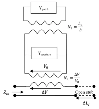
From Figure 11,
𝑌𝑌𝑡𝑡𝑝𝑝𝑒𝑒𝑗𝑗𝑡𝑡𝑢𝑢𝑗𝑗𝑒𝑒 = 𝑌𝑌1𝑁𝑁22− 𝑁𝑁12𝑌𝑌𝑝𝑝𝑡𝑡𝑡𝑡𝑠𝑠 ℎ (27)
𝑌𝑌1
Side 2
Yaperture YPatch
Side 1
𝑁𝑁1
𝑁𝑁2 1 1
∆𝐿𝐿𝑟𝑟
𝑁𝑁1=𝐿𝐿𝑏𝑏𝑡𝑡
𝑁𝑁2=∆𝑉𝑉𝑉𝑉 0
∆𝑉𝑉 𝑉𝑉0
𝑐𝑐𝑠𝑠𝑠𝑠 Open stub
Ypatch
𝑌𝑌1=𝑌𝑌𝑡𝑡𝑝𝑝𝑒𝑒𝑗𝑗𝑡𝑡𝑢𝑢𝑗𝑗𝑒𝑒 +𝑁𝑁1 2𝑌𝑌
𝑝𝑝𝑡𝑡𝑡𝑡𝑠𝑠 ℎ
𝑁𝑁22 (28)
𝑐𝑐1= 𝑁𝑁2 2
𝑌𝑌𝑡𝑡𝑝𝑝𝑒𝑒𝑗𝑗𝑡𝑡𝑢𝑢 𝑗𝑗𝑒𝑒 +𝑁𝑁12𝑌𝑌𝑝𝑝𝑡𝑡𝑡𝑡𝑠𝑠 ℎ (29)
Taking into account the open-circuited stub in Figure 9(a), the total input impedance is
𝑐𝑐𝑠𝑠𝑠𝑠 = 𝑁𝑁2 2
𝑌𝑌𝑡𝑡𝑝𝑝𝑒𝑒𝑗𝑗𝑡𝑡𝑢𝑢𝑗𝑗𝑒𝑒 +𝑁𝑁12𝑌𝑌𝑝𝑝𝑡𝑡𝑡𝑡𝑠𝑠 ℎ− 𝑗𝑗𝑐𝑐𝑜𝑜𝑠𝑠𝑜𝑜𝑡𝑡(𝑡𝑡𝐿𝐿𝑠𝑠) (30)
where 𝑐𝑐𝑜𝑜 is the characteristic impedance and 𝑡𝑡 is the
effective propagation constant on the microstrip feedline of open-circuited length 𝐿𝐿𝑠𝑠, which accounts for ∆𝐿𝐿𝑟𝑟.
According to [8], the transformation ratio 𝑁𝑁1 is equal to
the fraction of current flowing through the aperture over the total intensity:
𝑁𝑁1=𝐿𝐿𝑡𝑡𝑏𝑏 (31)
and
𝑁𝑁2 =�𝑤𝑤𝐿𝐿𝑡𝑡𝑒𝑒ℎ (32)
𝑌𝑌𝑝𝑝𝑡𝑡𝑡𝑡𝑠𝑠 ℎ = 2𝑌𝑌0= �(𝑗𝑗𝐺𝐺 +𝐵𝐵)+𝑗𝑗𝑌𝑌0𝑡𝑡𝑡𝑡𝑠𝑠𝑡𝑡 𝐿𝐿𝑝𝑝′
2 𝑌𝑌0+𝑗𝑗 (𝐺𝐺+𝑗𝑗𝐵𝐵 )𝑡𝑡𝑡𝑡𝑠𝑠𝑡𝑡𝐿𝐿𝑝𝑝′2
� (33)
The knowledge of 𝑌𝑌𝑝𝑝𝑡𝑡𝑡𝑡𝑠𝑠 ℎ enables the aperture admittance
to be determined using equation (17).
3. Simulation Results and Evaluation
In practice, IEEE 802.11 WiMAX standards consist of 3.5-GHz (3.3–3.6 GHz) and 5.5-GHz (5.25–5.85 GHz) frequency bands. The resulting input impedance, and return are simulated at 5 GHz centre frequency using MATLAB. The results are shown in Figures 12 to 15 and the comparison of the performance characteristics of the different feed techniques are summarised in table 1.
Figure 12. Input impedance of Aperture-feed patch antenna at centre frequency of 5GHz
Table 1. Characteristics comparison of different feeding techniques Characteristics Line feed Coaxial feed Aperture feed
Return Loss Less More Less
Resonant
frequency More Less Least
VSWR <1.5 1.4 to 1.8 ≈ 2
Polarization Poor Poor Excellent Ease of
fabrication Simple drilling needed Soldering and Alignment required
Reliability Better Poor due to soldering Good
Impedance
matching Easy Easy Easy
Bandwidth 2 – 5% 2 – 5% 21%
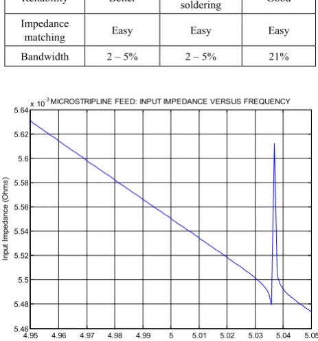
Figure 13. Input Impedance response of Microstrip line feed
Figure 14. Input Impedance response of Coaxial-feed 4.95 4.96 4.97 4.98 4.99 5 5.01 5.02 5.03 5.04 5.05
x 109 0
2000 4000 6000 8000 10000 12000
Frequency (GHz)
Input
Im
pedanc
e (
O
hm
s)
PLOT OF APERTURE FEED INPUT IMPEDANCE AGAINST FREQUENCY
4.95 4.96 4.97 4.98 4.99 5 5.01 5.02 5.03 5.04 5.05 x 10⁹ 5.46
5.48 5.5 5.52 5.54 5.56 5.58 5.6 5.62 5.64x 10
-3
Frequency (GHz)
Input
Im
pedanc
e (
O
hm
s)
MICROSTRIPLINE FEED: INPUT IMPEDANCE VERSUS FREQUENCY
4.95 4.96 4.97 4.98 4.99 5 5.01 5.02 5.03 5.04 5.05
x 109 0
0.5 1 1.5 2 2.5x 10
5
Frequency (GHz)
Input
Im
pedanc
e (
O
hm
s)
Figure 15. Return Loss response of Aperture-feed at 5GHz Centre frequency
Figure 16. Return Loss response of Lline feed technique
Figure 17. Return Loss response of Coaxial-feed
Maximum bandwidth can be achieved by aperture coupling, at an input impedance of around 50Ω. Figure 16 &
17 shows simulated input impedance of around 50Ω between
4.95 – 5.0 GHz.
4. Conclusions
It can be seen from Table 1 tha selection of the feeding technique for a microstrip patch antenna is an important decision because it affects the bandwidth and other parameters. A microstrip patch antenna excited by different excitation techniques gives different bandwidth, different gain, different efficiency etc.
Aperture coupled antennas are advantageous in arrays because they electrically isolate the feed and phase shifting circuitry from the patch antennas. The disadvantage is the required multilayer structure which increases fabrication complexity and cost.
REFERENCES
[1] T. Dunga et al; “Comparison of Circular and Rectangular Microstrip Patch Antennas”, IJCEA vol.2 Issue 4, pp. 187-197, July 2011.
[2] Q. Zhang, Y. Fukuoka, T. Itoh., “Analysis of a Suspended Patch Antenna excited by an Electromagnetically coupled Microstrip Feed” IEEE Transaction on Antennas and Propagation, Vol.33, n*8, August 1985, pp. 895-899.
[3] Robert W. Heath, Jr., Member, (2005), IEEE, and David J. Love Member, IEEE “Multimode Antenna Selection for Spatial Multiplexing Systems With Linear Receivers” IEEE transactions on signal processing, 53(8), pp 30423056. [4] Adarsh B. Narasimhamurthy and Cihan Tepedelenlioglu,
(2005), Member, IEEE,” Antenna Selection for MIMO OFDM Systems with Channel Estimation Error” IEEE transactions on vehicular technology, 58(5), pp 22692278. [5] D. Orban and G.J.K. Moernaut “The Basics of Patch
Antennas, Updated” September 29, 2009 edition of the RF Globalnet (www.rfglobalnet.com) newsletter.
[6] Charles Uzoanya Ndujiuba, Oluwadamilola Oshin, Nsikan Nkordeh “MIMO Deficiencies Due to Antenna Coupling”, International Journal of Networks and Communications 2015, 5(1): 10-17 DOI: 10.5923/j.ijnc.20150501.02.
[7] Gonca CAKIR, Levent SEVGI; “Design, Simulation and Tests of a Low-cost Microstrip Patch Antenna Arrays for the Wireless Communication”; Turk J ElecEngin, VOL.13, NO.1; 2005.
[8] Leo G. Maloratsky; “Reviewing the Basics of Microstrip Lines”; Microwave and RF; March 2000.
[9] Indrasen Singh, Dr. V.S. Tripathi; “Microstrip Patch Antenna and its Applications: a Survey”; Available [email protected]; IJCTA; SEPT-OCT 2011.
[10] Marek Bugaj, Rafal Przesmycki, Leszek Nowosielski, and Kazimierz Piwowarczyk; “Analysis Di®erent Methods of Microstrip Antennas Feeding for Their Electrical Parameters”; PIERS Proceedings, Kuala Lumpur, MALAYSIA, March
4.95 4.96 4.97 4.98 4.99 5 5.01 5.02 5.03 5.04 5.05
x 109 -0.12
-0.1 -0.08 -0.06 -0.04 -0.02 0
Frequency (GHz)
R
et
ur
n Los
s(
dB
)
APERTURE FEED RETURN LOSS AGAINST FREQUENCY
4.95 4.96 4.97 4.98 4.99 5 5.01 5.02 5.03 5.04 5.05 x 10⁹ -2.48
-2.46 -2.44 -2.42 -2.4 -2.38 -2.36x 10
-3
Frequency (GHz)
R
et
ur
n Los
s (
dB
)
MICROSTRIPLINE FEED: RETURN LOSS VERSUS FREQUENCY
4.95 4.96 4.97 4.98 4.99 5 5.01 5.02 5.03 5.04 5.05
x 109 -0.018
-0.016 -0.014 -0.012 -0.01 -0.008 -0.006 -0.004 -0.002 0
Frequency (GHz)
R
et
ur
n Los
s (
dB
)
27{30, 2012.
[11] Ahmed H. Reja; “Study of Microstrip Feed Line Patch Antenna”; Eng& Tech Journal, Vol 27, No.2; 2009.
[12] Rachmansyah, Antonius Irianto, and A. Benny Mutiara; “Designing and Manufacturing Microstrip Antenna for Wireless Communication at 2.4 GHz”; International Journal of Computer and Electrical Engineering, Vol. 3, No. 5, October 2011.
[13] John R. Ojha and Marc Peters; “Patch Antennas and Microstrip Lines”, Microwave and Millimeter Wave Technologies: Modern UWB antennas and equipment; www.intechopen.com; June 2012.
[14] Marwa Shakeeb; “ Circularly Polarized Microstrip Antenna”; The Department of Electrical and Computer Engineering Concordia University, Montreal, Quebec, Canada; Master’s Thesis, December 2010.
[15] Nagraj Kulkarni, S. N. Mulgi, S. K. Satnoor; “Design and Development of simple low cost Rectangular Microstrip Antenna for multiband operation”; International Journal of Electronics and Electrical Engineering; Volume 1, Issue 1 ISSN : 2277-7040; March 2012.
[16] Elena Pucci, Ashraf UzZaman, Eva Rajo-Iglesiasand Per-Simon Kildal; “New Low Loss Inverted Microstrip Line using Gap Waveguide Technology for Slot Antenna Applications”; Proceedings of the 5th European Conference on Antennas and Propagation, EUCAP 2011. Rome; 11-15 April 2011.
[17] Q. Zhang, Y. Fukuoka, T. Itoh., “Analysis of a Suspended Patch Antenna excited by an Electromagnetically coupled Microstrip Feed” IEEE Transaction on Antennas and Propagation, Vol.33, no.8, August 1985, pp. 895-899. [18] D. Orban and G.J.K. Moernaut “The Basics of Patch
Antennas, Updated” September 29, 2009 edition of the RF Globalnet (www.rfglobalnet.com) newsletter.
[19] K. Jagadeesh Babu, Dr. K. SriRama Krishna, Dr. L. Pratap Reddy; “A Modified E Shaped Patch Antenna For MIMO Systems”; International Journal on Computer Science and Engineering, 2(7), pp 24272430; 2010.