_____________________________________________________________________________________________________
Wafer Tape Selection Analysis for Adhesion Problem
Mitigation
Bryan Christian S. Bacquian
1and Frederick Ray I. Gomez
1*1
STMicroelectronics Inc., Calamba City, Laguna, 4027, Philippines.
Authors’ contributions
This work was carried out in collaboration between both authors. Both authors read and approved the final manuscript.
Article Information
DOI: 10.9734/JERR/2019/v6i416958
Editor(s):
(1) Dr. David Armando Contreras-Solorio, Professor, Academic Unit of Physics, Autonomous University of Zacatecas, Mexico.
Reviewers:
(1) Boyan Karapenev, Technical University of Gabrovo, Bulgaria. (2)J. Ladvánszky, Ericsson Telecom Hungary, Hungary. Complete Peer review History:http://www.sdiarticle3.com/review-history/50519
Received 01 June 2019 Accepted 11 August 2019 Published 19 August 2019
ABSTRACT
Wafer passivation or the protective layer of the internal circuitry of the die plays a major role of providing protection and the isolation of electrical stability of the active circuit on the top area of the wafer. Passivation is normally a screen of an oxide layer on the surface of the silicon wafer or the carrier of internal circuitry of the die. Passivation is normally in the form of polyimide or a glass material. From the wafer structure, it is important to cover the active circuit to ensure no other noises will be induced to the wafer. Inclusion of the passivation layer will help maximize the functionality of the semiconductor device thus eliminating noises coming from the external sources. As the integrated circuit (IC) package goes thinner, the requirement of having the active circuit or the die thinner is the main concern during the wafer preparation process. Wafer backgrinding or wafer thinning is the focal process involved to satisfy such requirement. Prior performing the wafer thinning process, the application of tape, normally in a form of polyolefin or polyvinyl chloride should be performed to eliminate contamination and protects the active layer of the wafer during the process. However, there should be enough adhesion between the wafer and the thinning tape itself. High adhesion strength may lead to adhesive remains or worst, passivation will be peeled off from the active layer of the wafer.
Adhesion to the passivation layer should be properly evaluated and monitored in such way that will eliminate adhesive remains during detaping process after wafer thinning. The effect of adhesion strength could be predicted by properly selecting thinning or protective tape to be used. Higher
adhesion strength could be achieved but due to criticality of passivation to tape adhesion, ultra-violet (UV) process should be included to substantially decreased the adhesion. The importance of UV exposure is also discussed on this paper.
Keywords: Wafer tape; wafer preparation; pre-assembly; ultraviolet; passivation; adhesion.
1. INTRODUCTION
Wafer thinning is one of the critical pre assembly process in which wafers are grinded or thinned to a required thickness to cater the package requirements. However, it is important to protect the active layer of the wafer, thus applying an adhesive tape is a must. There should be no water penetration during the grinding or thinning process and no contamination on the thinning tape so that the active layer is totally intact after thinning process. In line with that, the protective tape should have three critical characteristics: Suitable adhesion, Easy de taping and good uniformity after thinning.
Different silicon technologies have been developed according to its application. Wafer could have different surface finish and the common is the application of a passivation layer. The peeling off of the wafer passivation together with the protective tape during detaping process is one major concern. With this, the assembly manufacturing plant carefully analyzed the criticality of tape adhesion. Three (3) different protective tapes are evaluated and prudently select the suitable protective tape to this wafer technology. The evaluation will involve on how proper selection of the protective tape adhesion strength will eliminate wafer passivation removals.
The importance of removing properly the protective tape is to ensure the workability and good response of the electrical performance of our integrated circuit manufacturing. Several problems may arise like broken dies, contamination, lifted wires and delamination that may cause malfunction of the integrated circuit. The study will help the practitioners of the integration circuit manufacturing to properly select protective tapes to eliminate problems during the wafer preparation process, specifically for wafer with passivation.
1.1 Wafer Passivation
Wafer passivation is normally the masking of an oxide layer on the surface of the active layer of
the wafer. Passivation is important to provide electrical stability and insulation to the environment. There are two common forms of passivation which are polyimides and silicate glass. Though on the specific silicon wafer technology has been developed polyimide resin is used.
Polyimides are a polymer of imide monomers [1], normally on orange or yellow color appearance. Exceptional characteristics of polyimides are thermal stability, good chemical resistance, and excellent mechanical properties. Polyimides have good mechanical elongation and tensile strength. The polyimide layers have good mechanical elongation and tensile strength, which helps provide good adhesion of the deposited metal layer to the polyimide. The minimal interaction of the polyimide and the deposited metal and the thermal stability helps provide good and reliable insulation of the wafer to the environmental stresses [2]. Normally in the wafer fabrication process, passivation is placed on the top surface of the silicon wafer as shown in Fig. 1.
Fig. 1. Wafer structure cross-sectional view
1.2 Wafer Tape
Fig. 2. Graphical representation of types of protective tape
Conventional protective tapes have normally a much lower adhesion strength compared to UV type tapes. Hence, a little contamination could be transferred to the wafer surface. On the other hand, UV type tapes show no water penetration and wafer breakage during thinning due to its higher adhesion strength compared to conventional types. Also, UV type tape requires additional exposure to ultra violet radiation that will help reduce its adhesion strength, will therefore aid the ease of detaping process. Due to peeling off of passivation from the active circuit of the wafer, three different protective tapes have been selected to check different responses during detaping process.
2. LITERATURE REVIEW
Wafer thinning is the thinning of semiconductor wafers by removing material from the unpolished wafer back side. Wafers are often fabricated thicker than necessary, normally at 600 to 750µm thick, and this has been determined by the stresses during processing and the requirement of handling robustness. During the back end process, there is a need for thinning the wafers in order to meet the package requirements and at the same time, the functionality of the IC package [3-5]. In connection, most of IC assembly wafer thickness is reduced to around 50% thinner, partly for mechanical reasons and improve thermal transfer [4-6].
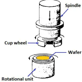
There are several methods that are presently being used for thinning wafers; the most popular is the well-established mechanical thinning and polishing technique. As illustrated in Fig. 4, a standard wafer thinner has a rotating work chuck table wherein the wafer or the work piece is being positioned; diagonally a spindle will help the rotating diamond cup wheel turn towards the chuck table [6-7]. The downward movement of
the spindle carrying the cup wheel removes silicon material from the surface of the wafer, thus creating a flat surface. The wheel alignment and chuck table planarity plays a major role on attaining uniformity of wafer thickness. However, it is difficult to measure this setting so post-thinning measurements are made using a non-contact capacitive probe. The parameter normally assessed is total thickness variation (TTV), where a typical target value is <10 µm.
Fig. 3. Schematic of a rotational wafer thinner
Fig. 4. Two-step wafer thinning process
After thinning process, the protective tape should be removed in preparation for the wafer sawing. There should be no adhesive residuals that may lead to wafer surface contamination. Therefore, an extensive evaluation should be performed to suitably select the protective tape that will surpass all wafer preparation requirements, specifically adhesion strength that will eliminate surface contamination, ease of detaping and will not incur wafer breakage.
3. EXPERIMENTATION
3.1 Protective Tape Selection
Wafer with polyimide passivation, on a 200 mm diameter Complementary metal-oxide-semiconductor or CMOS Silicon technology outline, have been used to evaluate and select appropriate Protective tape to eliminate detachment of the wafer passivation after de taping process. All 3 wafers are all received with 725 µm wafer thickness will be thinned on the same final thickness of 105 µm. Also, same
machine is used, with installed UV curing and de taping process up to wafer mounting, for all the three evaluation wafers. The thinning machine have also same machine setting of same mounting and detaping chuck table temperature of 33.5 ± 5°C and 40-50°C respectively, across the evaluation.
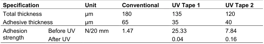
Three different thinning tapes presented in Table 1 have been selected to appropriately evaluate the best eliminator of peeling issue of the passivation from the active layer of the wafer. The first protective tape is on a conventional type and been used on the released process for complementary metal-oxide semiconductor (CMOS) wafers. Adhesion strength of the conventional type is compared lower than the two other protective tape. The other 2 types are both on UV type protective tape, which differs on adhesion strength ratio (before and after UV) but almost on the same total and adhesive thickness. UV Tape 1 is designed to have higher adhesion strength before UV but a lower adhesion after UV.
Table 1. Protective tape configuration
Specification Unit Conventional UV Tape 1 UV Tape 2
Total thickness µm 180 135 120
Adhesive thickness µm 65 35 40
Adhesion strength
Before UV N/20 mm 1.47 25.33 7.84
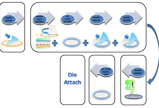
3.2 Process Flow
The evaluation of the three wafers were processed on a single thinning machine with equipped UV curing and de taping process. The evaluation has been sub divided into two processes. The first process in Fig. 5 involves the procedure of normal thinning – detaping
process flow with conventional tape type as protective tape. Another process show in Fig. 6 involves the activation of UV curing after thinning. This will lessen the adhesion strength of the two UV curable type of protective tape prior detaping process. The result will be determined by process elimination and be based according to the visual inspection criteria.
Fig. 5. Pre-assembly process flow for conventional protective tape
4. RESULTS AND DISCUSSION
4.1 Conventional Type Protective Tape
Conventional type protective tape encountered broken wafer or detachment of the passivation layer after detaping as depicted in Fig. 7. Therefore, the amount of adhesion strength at 1.47 N/20mm is too sticky for the polyimide and thinning tape.
4.2 UV-Curable Type Protective Tape
The two UV curable types are processed on same process flow with the activation of UV curing after thinning. UV type 1 having higher adhesion strength during thinning and a much
lower adhesion after UV curing have not encountered peeling of the passivation in Fig. 8.
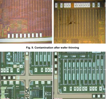
Meanwhile, adhesive remains/contamination on the passivation surface as well as on the bond pad was observed during the inspection using a high magnification microscope in Fig. 9.
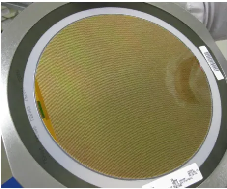
The affected wafer was continuously processed until wafer saw process but still adhesive/ contamination is present on the passivation surface after wafer sawing. On the other hand, UV type 2, with higher adhesion strength after the UV exposure and lower adhesion before UV, showed good response after detaping process. As a result, there is none anomaly or adhesive contamination found in Fig. 10 on the passivation and even on the bond pad.
Fig. 7. Detachment of the passivation layer after wafer detaping
Fig. 9. Contamination after wafer thinning
Fig. 10. No adhesive contamination after detaping process
5. CONCLUSION AND RECOMMENDA-TIONS
Based on the evaluation, Conventional type protective tape will aggravate the peeling off of the passivation from the active layer of the wafer. However, UV type protective tapes will eliminate such peeling problem of the passivation by lower adhesion strength after UV exposure.
Lower adhesion strength before UV exposure and higher adhesion after UV greatly helped to mitigate the peeling off problem of passivation from the active layer after detaping. Hence, maintaining low adhesion strength of the UV curable type protective tapes, both before and after UV exposure, will also eliminate adhesive remains after detaping process.
Based on the results, it is highly recommended to use a UV-curable type protective tape on a
polyimide based passivation to eliminate detachment of the passivation after detaping process. It is also important to have the proper selection of the appropriate protective tape to be used and this involves carefully understanding the adhesion strength ratio between before and after UV exposure.
applied on the edge of the wafer during thinning. For ensuing critical processes like that of the wafer saw, discussions in [5,8-9] are helpful to prevent or eliminate defects related to wafer preparation. Furthermore, it is highly important that the assembly manufacturing processes ensure appropriate ESD checks and controls. Learnings shared in [10] are very helpful to realize proper and effective ESD-related controls.
ACKNOWLEDGEMENTS
The authors would like to express appreciation and gratitude to the Central Engineering and Development – New Product Introduction (NPI) team and colleagues of STMicroelectronics
Calamba who have greatly contributed to the success of the work. The authors are
thankful to the Management Team for the great support.
COMPETING INTERESTS
Authors have declared that no competing interests exist.
REFERENCES
1. Merriam-Webster, Incorporated, “Polyi-mide”; 2019.
2. Krakauer D. Digital isolation offers compact, low-cost solutions to challenging
design problems. Analog Dialogue. 2006; 40.
3. STMicroelectronics. Visual criteria for sawed wafers and dice. rev. 26.0; 2019. 4. STMicroelectronics. Assembly and EWS
design rules for wire bond Interconnect dice. rev. 53.0; 2018.
5. Bacquian BC, Gomez FR. A study of wafer backgrinding tape selection for SOI wafers. Journal of Engineering Research and Reports. 2019;6(2):1-6.
6. Combs E. The back-end process: Step 3 - Wafer Backgrinding; 2002.
7. “Wafer breakage due to backgrinding”. The Cutting Edge Technical Newsletter; 2008. 8. Sumagpang A, Gomez FR. Line stressing
critical processes optimization of scalable package passive device for successful production ramp-up. Journal of Engineering Research and Reports. 2018; 3(1):1-13.
9. Bacquian BC, Gomez FR. A study of vacuum efficiency for silicon on insulator wafers. Journal of Engineering Research and Reports. 2019;6(1):1-6.
10. Gomez FR, Mangaoang T. Elimination of ESD events and optimizing waterjet deflash process for reduction of leakage current failures on QFN-mr leadframe devices. Journal of Electrical Engineering, David Publishing Co. 2018;6(4):238-243.
© 2019 Bacquian and Gomez; This is an Open Access article distributed under the terms of the Creative Commons Attribution License (http://creativecommons.org/licenses/by/4.0), which permits unrestricted use, distribution, and reproduction in any medium, provided the original work is properly cited.
Peer-review history: