ISSN: 2393-8366
657
Design of VHBCSE Based Constant Multiplier for
FIR Filter Using Reversible Gates
Jismy Theresa1, Manju V.M2, Rachana M. K3 1
PG Scholar,2,3Assistant Professor, 1,2,3
Department of Electronics and Communication, IES College of Engineering, Thrissur, India [email protected],[email protected]2,[email protected]3
Abstract: Nowadays digital filters are widely used in communication system as well as signal processing. Re configurability and low complexity are the two key requirements of FIR filter. In recent SDR technology, dynamically reconfigurable filters are needed to be designed. This project proposes VHBCSE based reconfigurable FIR (finite impulse response) filter using reversible gates .Using VHBCSE first of all a 2-bit binary common sub-expression elimination algorithm applied vertically across adjacent coefficients on the 2-D space of matrix that includes coefficient next applying 4-bit and 8-bit BCSE algorithm horizontally within each coefficient. And all this adder and multiplexer operation occurring in the system are replaced with reversible gates. Using reversible circuit energy dissipation in form of heat and power can be saved. The system implemented using XILINX ISE 14.2 tool by VHDL language.
Keywords: VHBCSE Algorithm, SDR system, MCM 1. Introduction
In digital signal processing and communication systems, FIR filters are the essential one. There are so many fields such as image and video processing, biomedical signal processing systems and wireless communication are includes FIR filters. Adder, multiplier and delay element are the elements in FIR filters. In that multiplier are the most area and power consuming components. So for realizing FIR filters, hardware cost of multipliers is important one. The amount of power consumption and computation of FIR filter are directly proportional to the order of the filter.
The multiplication operation in FIR filters is performed between one particular variable and many constants, that particular variable is input and constants is the coefficients, and known as multiple constant multiplication. The earlier proposed algorithm to implement MCM is graph based and common sub expression elimination algorithm. These algorithms on fixed set coefficients are not suitable for the application like SDR system. This is because of mainly two reasons one is coefficient of filters in SDR system are dynamically programmable based on need of different standard and the other one is highly computationally efficient platform needed.
ISSN: 2393-8366
658
horizontally within each coefficient and all this adder and multiplexer operation occurring in the system are replaced with reversible gates.
Energy dissipation is one of the problems associated with electronic circuits. The device is growing day by day so need low power circuits. By using reversible circuit lose of information during computation will reduces and it can be performed only when the system comprises of reversible gates. When replacing the entire adder and multiplexer by reversible gates total power in the system is reduces. So the emerging nanotechnology can make use of the new FIR filter.
The organization of the paper as follows. In section II .description of FIR filter have been discussed In section III, concepts of VHBCSE algorithm have been discussed. The importance of reversible gates and various types of reversible gates used in system have been narrated in section IV. Architecture of proposed VHBCSE system with reversible gates has been described in section V. Software implementation results along with discussions on comparison of my results with other reported implementation have been proposed in section VI.
2. FIR Filter
A finite impulse response (FIR) filter is a filter whose impulse response (or response to any finite length input) is of finite duration, because it settles to zero in finite time.
For a causaldiscrete-time FIR filter of order N, each value of the output sequence is a weighted sum of the most recent input values.
𝑦[𝑛] = 𝑏0𝑥𝑥[𝑛] + 𝑏1𝑥[𝑛 − 1] + 𝑏2𝑥[𝑛 − 2] − ∓𝑏𝑁𝑥[𝑛 − 𝑁]
𝑦[𝑛] = ∑ 𝑏𝑖∗ 𝑥(𝑛 − 𝑖)
𝑁
𝑖=0
Where, x[n] is the input signal, y[n] is the output signal ,𝑏𝑖 are the filter coefficients also known as tap weights, that make up the impulse response , N is the filter order
Figure.1. A direct form discrete-time FIR filter of order N.
3. Multiplication Using VHBCSE Algorithm
ISSN: 2393-8366
659
3.1. Architecture of the VHBCSE Algorithm Based Constant Multiplier
The data flow diagram of the vertical-horizontal BCSE algorithm based constant multiplier (CM) design is shown in Fig.2. The designed multiplier has the length of the input (Xin) and coefficient (H) as 16-bit and 17-bit respectively .The output of multiplication is assumed to be 16-bit long. The sampled inputs are stored in the register first and then the coefficients are stored directly in the LUTs.
Figure.2. Data flow diagram of CM using VHBCSE Algorithm
4. Reversible Gates
If the input vectors can retrieved from output vectors and one to one correspondence with input and output then the circuit is said to follow reversible logic. There are many types of reversible gates are there. Each of them is differ because of their function. Basic reversible logic circuit is shown in figure 3
An N*N reversible system can be represented as
I = (i1, i2, i3 --- iN)
O= (o1, o2, o3 --- o N)
Here ‘I’ represent input vectors and ‘O’ represents output vectors.
Figure.3. Basic reversible logic circuit
ISSN: 2393-8366
660
corresponding outputs. The characteristics of reversible logic should determine by some of parameters that are constant input and garbage output.
4.1. FREDKIN Gate
The Fredkin gate, also known as CSWAP gate is a computational circuit suitable for reversible computing. It was invented by Edward Fredkin. It is universal, which means that any logical or arithmetic operation can be constructed entirely of Fredkin gates. The Fredkin gate is a circuit or device with three inputs and three outputs that transmits the first bit unchanged and swaps the last two bits if, and only if, the first bit is 1.
Figure.4. Fredkin gate
4.2 .PERES Gate
A Peres gate can be used as half adder and full adder. It has three gate inputs and outputs in case of full adder. In case of full adder, Peres gate has four inputs and four output. Its quantum cost is five.
Figure.5. Peres gate
5. Architecture of Proposed VHBCSE Using Reversible Gates
The data flow diagram of VHBCSE algorithm is depicted in fig 2. It is the design of the input (Xin) and coefficient (H) as 16-bit and 17-bit respectively while the output is assumed to be 16-bit long. The functionality of the hardware architecture of different blocks used in VHBCSE by using reversible gates are explained below.
5.1. Sign Conversion Block
This block is needed to give support the signed decimal format data representation input as well as coefficients. The architecture of sign conversion block is shown in figure 6.
ISSN: 2393-8366
661
Here the 1’s complemented circuit is used to generate the inverted version of 16 bit coefficient. Here Fredkin gate is work as 2:1 multiplexer. Depending on the value of most significant bit of the coefficient, one 16 bit Fredkin gate produces the multiplexed coefficient.
5.2. Partial Product Generator (PPG)
Here shift and add based technique is used to generate the partial product. It will be summed up in the following layers for producing the final multiplication result. For the coefficient of 16-bit length, 8 partial products of 17, 15, 13, 11, 9, 7, 5, and 3 bits (P8-P1) will be produced by right shifting the first partial product (P8) by 0, 2, 4, 6, 8, 10, 12, and 14 bits respectively. This is shown in figure 7.
Figure.7. Block diagram of partial product generator unit
5.3. Control Logic Generator
This block takes the multiplexed coefficient that is from Fredkin gate (Hm [15:0]) as its input and groups it into one of 4-bit each (Hm [15:12], Hm [11:8], Hm [7:4], and Hm [3:0]) and another of 8-bit each (Hm [15:8], Hm [7:0]). Seven control signals produced from the CL generator block depending on the equality check for 7 different cases. The control signal for 8-bit equality check is seen to be produced through the control signals generated from the 4-bit equality check.
5.4 . Multiplexer Unit
This multiplexer unit is used to select the suitable data produced from the PPG unit depending on the coefficient's binary value. At layer-1, to produce the partial products according to the 2-bit BCSE algorithm eight 4:1 multiplexers are required and it applied vertically on the MAT. The eight multiplexer’s width are 17, 15, 13, 11, 9, 7, 5, and 3-bit each instead of 16-bit for all, through this hardware and power consumption are reduces.
ISSN: 2393-8366
662 5.5. Controlled Addition Layer 2
The generated partial products (PP) from eight groups of 2-bit BCSs are added up for the final multiplication results, it is performed in three layers. As said in the BCSE algorithm, layer-2 requires four addition (A1-A4) using Peres gates operations to sum up the eight PPs. In place of direct addition of these PPs, the controlled addition operations are performed at layer 2. These adders (A1-A4) are directed depending on the control signals (C1-C6). These control signals were generated based on 4-bit BCSE from the control signal generator block.
Figure. 9. Block diagram of controlled addition layer 2
5.6. Controlled Addition At Layer 3
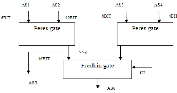
The four multiplexed sums (AS1, AS2, AS3 and AS4) generated from layer-2 Using Peres and Fredkin reversible gates are now added up in layer-3. In this algorithm, instead of direct addition, controlled additions are performing. For this reason, this addition (A6) is controlled by the control signal (C7) which has been produced based on 8-bit BCSE from the CS generator block.
Figure.10. Block diagram of controlled addition layer 3
5.7. Final Addition Layer 4
ISSN: 2393-8366
663
Figure.11. Proposed Reconfigurable constant multiplier architecture
6. Software Implementation and Conclusion
The VHBCSE algorithm based reconfigurable FIR using reversible gates shown in figure.11 has been coded using VHDL language using Xilinx 14.2 synthesis tool. Nowadays FIR filter has wide application in digital signal processing world like digital up counter, down counter etc. This proposed 4 tap FIR filter design possesses 10% to 15% reduction in power and area compared with earlier VHBCSE system. Xilinx Xpower EDA tool has been used to calculate dynamic power consumption of the filter.
This architecture gives high speed filters and results in low area and thus low power filter implementations.Due to this algorithm, it provides the flexibility of changing the filter coefficient word lengths dynamically. For supporting the signed decimal data representation and increase the efficiency this algorithm using reversible gates more appropriate for the coming generation skilful systems like software defined radio.
Acknowledgement
I express my sincere thanks to my guides Ms.Manju V.M and Ms.Rachana M. K. for their valuable guidance and useful suggestions, which helped me in the project work.
REFERENCES
[1] IndranilHatai, IndrajitChakrabarti, and Swapna Banerjee, “An Efficient Constant Multiplier Architecture Based on Vertical-Horizontal Binary Common Subexpression Elimination Algorithm for Reconfigurable FIR Filter Synthesis” IEEE Transactions on Circuits And Systems 2015
[2] S. J. Darak, S. K. P. Gopi, V. A. Prasad, and E. Lai, “Low-complexity reconfigurable fast filter bank for multi-standard wireless receivers,” IEEE Trans. Very Large Scale Integr. (VLSI) Syst., vol. 22, no. 5, pp. 1202–1206, May 2014
ISSN: 2393-8366
664
[4] M. Aktan, A. Yurdakul, and G. Dundar, “An algorithm for the design of low-power hardware-efficient FIR filters,” IEEE Trans. Circuits Syst. I, Reg. Papers, vol. 55, pp. 1536– 1545, Jul. 2008
[5] R.Mahesh and A. P. Vinod, “New reconfigurable architectures for implementing FIR filters with low complexity,” IEEE Trans. Comput. Aided Design Integr. Circuits Syst., vol. 29, no. 2, pp. 275–288, Feb. 2010
[6] Anigha Johnson and Manju V.M.” Implementation of an efficient ALU using Reversible Logic Gate” International Journal of Advanced Research in Electronics and Communication Engineering (IJARECE) Volume 5, Issue 7, July 2016.
ABOUT AUTHORS
Jismy Theresa, currently pursing PG in VLSI Design from IES college of Engineering, Thrissur, Kerala, India. She received her B.Tech in Electronics and Communication from Vidya Academy of Science &Technology, Thrissur, Kerala, India in 2015. Her interested areas are testing and verification and VLSI design.
Mrs. Manju V M, currently working as an Assistant Professor/PG coordinator in Department of Electronics and Communication Engineering at IES College of Engineering, Thrissur, Kerala, India.She received her M.E degree in VLSI Design from Anna University, Trichi in 2009. She is a member of ISTE and IEEE. Her interested research areas are low power VLSI design and digital system design.