5425
Abstract: PWM strategies are key options for extracting the quality controllable outputs from the VSI. The objectives involved in the different PWM strategies are improving the primary indices namely, enhancing the fundamental components, reducing the total harmonic distortion, minimizing the switching loss, specific removal of harmonic components etc… while the secondary Issues like suppressing the electromagnetic interference, spreading the harmonic power etc., are also to be considered in contemporary applications. This paper is disquiet about an enhancing the harmonic power dispersal of PWM strategies. The RPWM strategies cover non-predictable harmonic pattern and called as non-deterministic PWM strategies. The inverter is working under RPWM which generate the output harmonic spectra isolated and constantly distributes across frequencies and acoustic noise is also reduced. The paper has proposed a host of carrier based RPWM schemes to enhance the performance of the VSI and implemented them in FPGA involved digital platform. Power dissipation and Speed are presented in detail in term of resource use in FPGA. The RPWM technique is simulated by using time efficient co-simulation (Mat lab-Simulink) methodology.
Keywords: PWM techniques; Harmonics; switching loss; Random PWM; FPGA; VSI; acoustic noise; MATLAB/Simulink, Hardware Implementation.
——————————◆——————————
1.
INTRODUCTION
The demand of higher rating power electronics like drives has increasingly grown in the recent years. In an adjustable speed ac drive, it has become very essential to control the ac voltage and frequency with specified distortion level. The line current becomes a twisted waveform when an induction motor is fed from such a motion. Harmonics therefore power the MMF and improve the harmonics with the same air gap permeance. Because of the radial magnetic forces produced by the harmonics, strong vibrations occur in the rotor and core system. [3] Consequently, vibration, acoustic noise, alternating torque and losses due to the current harmonics have been increased.Using a high switching frequency is a common method of reducing noise so that the produced sound is ultrasonic. But this can cause extreme losses in the switching devices and extreme stress. Therefore, the tricky task is to find a proposed PWM (RPWM) scheme that eliminates acoustic noise by suppressing the VSI output's leading harmonics. The main objective of these RPWM systems is to disperse the harmonic power throughout the spectrum instead of collecting at multiple frequencies of the carrier. The software specifications are higher than the performance of the current RPWM methods. [6] In an induction motor drive fed VSI application, the existing RPWM schemes need to be improved in the performance for enhanced distribution of harmonic power.
The major objectives of this proposed work is to:
1. Study the randomization levels of different RPWM in terms of harmonic spread factor and harmonic magnitudes etc.
2. Develop and design the new digital PWM pulses of RPWM techniques by VHDL Language.
3. Verify the functionality by using ModelSimSE 6.3f digital simulator
4. Verify the performance of FPGA by using the navigator tool Xilinx Project.
5. Prove the inverter functionality by combining MATLAB and Modelsim simulation. Create comparative study of PWM performance in terms of THD, HSF and fundamental component values of output voltage.
6. Corroborate the simulation results of existing and proposed RPWM schemes in the designed experimental set up (three phase VSI).
7. As a whole, this project aims at improving the performance of RPWM schemes applicable to VSI drive and calculating a formulaic, prudent, digital implementation of such schemes.
2.
VOLTAGE SOURCE INVERTERS
Nowadays, inverter plays a vital role in every power converter as well as industrial applications. It is broadly divided into two types such as CSI and VSI. Out of which, VSI is more popular used power electronics converter broadly utilized power rating from various kilowatt to megawatt range. Inverter is a power electronics converter used to converts a fixed DC voltage to the variable three phase AC voltage with convenient frequency and magnitude. PWM based VSIs are usually used to control the shaft torque/ speed /position of AC motor drive applications and it have surge with stand potential in the inverter drives. [8] High power and medium voltage drives have established the wide applications in the industries. Mainly PWM-VSIs are used in Uninterruptible Power Supplies applications, regenerative drive applications (Umanand 2009), etc… and some other applications include static VAR compensators.
___________________________________
• Jegadeeswari .G, Department of Electrical and Electronics Engineering, AMET Deemed to be University, Chennai, India. Email: [email protected]
• Kirubadurai.B, Department of Aeronautical Engineering, Vel Tech Dr. Rangarajan Dr. Sagunthala R&D Institute of Science & Technology, Chennai, India. Email: [email protected]
• D. Lakshmi, Department of Electrical and Electronics Engineering, AMET Deemed to be University, Chennai, India. Email: [email protected]
5426
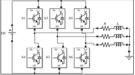
Fig 1: Three Phase Voltage Source Inverter
3.
INFLUENCE OF PWM TECHNIQUES
The pleasant quality of diversified power converters, solid-state power semiconductor devices, specification-oriented pulse width modulation (PWM) theories and shade digital controllers have driven the migration of conventional power controllers to solid state arena. In further, drives are imperative component in the motion control, where not only the required mechanical characteristics are obtained from the motor and also the quality of the electrical power involvement have made conducive. In midst of the different drives, the application of voltage source inverters (VSIs) is plenary. An inverter's main objective is to produce a sinusoidal AC voltage with frequency and varying amplitude from a DC source. PWM strategies are the key options for extracting the quality controllable outputs from the VSI and have received a dominant position in the last few decades (Mahesh et al. 2009; Seung-Wook et al. 2016). [5] Many PWM schemes have been developed and implemented successfully for different applications. Even though in due course, there are different scales of classification in PWM techniques (Jagadish et al. 2012), [7] therefore, the certainty in arriving the harmonic profile at particular input and control structures spur a variant categorization. The PWM schemes mentioned hitherto offer a well-defined, predictable harmonic profile and it is called as deterministic PWM schemes
3.1 SINUSOIDAL PULSE WIDTH MODULATION
SPWM is one of the main proven and trouble-free methods used in drives for motor control and power inverter from all PWM schemes. [10] Its major features can be summarizing as sinusoidal-triangle wave relationship. Figure illustrates that a sinusoidal wave is just separated by a triangle wave, and if the instantaneous value of the triangle wave is much lower than that of the sinusoidal waveform, but the PWM output signal will be high, then it will show ' 1 ' otherwise it will be low, showing ' 0. ‘[14] Whenever the sine wave meets the triangle wave, the switch is created. Therefore the different positions which consequence the changeable output waveform with the duty cycle.
Fig 2. SPWM waveform generation
3.2 RANDOM PULSE WIDTH MODULATION
By adding two triangular carriers we can achieve random carrier, each one is similar to other fixed frequency, however of opposed phase. [3] Determination of random set of two carriers is achieved by “0” or “1” which states that pseudo random binary sequence which is listed in Table 1.1.
Table 1.1 Truth of the Multiplexer
PRBS Status MUX Output
0 C
1 C BAR
Fig 3. Random bit generation
5427
Fig 5. Carrier Generation with Random bit
Fig 6. Pulse Generation of RPWM with Random bit
Figure 5 shows the output produced by the random carrier (fc=3 kHz). Figure 6 displays all the generation of switching pulses with the correct carrier and reference wave. In addition, the Random bit produced every 3 kHz, as shown in Figures 3 and 4.
3.3 INTRODUCTION TO FPGA
FPGAs allow designers to change their designs in the proposed process extremely delayed – they have been developed and implemented in the field even behind the end formation. [4] Xilinx FPGAs, on the other hand, require the removal of field updates, the elimination of costs related to manual upgrading or the re-design of electronic systems. FPGAs have evolved far away from the basic capabilities which are accessible in their predecessors, and include hard blocks of usually worn functionality such as DSP, clock management, and RAM. [11] The following are the essential mechanism in an FPGA: 1. complete clock management 2. Interconnect 3. Select IO (IOBs) 4. Memory Configurable logic blocks and 5. Configurable logic blocks as shown in Figure 2.
Fig 7. FPGA Block Structure
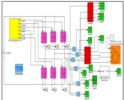
Fig 8: SIMULINK Model of Three Phase Inverter
Harmonic Spectrum Results
The Harmonics can be verified by using FFT window. 50 Hz line to line voltage cycle has been worn to calculate harmonics and their effects. The simulation outcomes are illustrated for a mixture of modulation indexes (ma) from 0.1 to 1.2. The harmonic spectrum of SPWM has shown in figure 9.1 to 9.12
Fig 9.1 Harmonic Spectrum-SPWM, ma=0.1 and mf=50
5428
Fig 9.3 Harmonic Spectrum-SPWM, ma=0.3 and mf=50
Fig 9.4 Harmonic Spectrum-SPWM, ma=0.4 and mf=50
Fig 9.5 Harmonic Spectrum-SPWM, ma=0.5 and mf=50
Fig 9.6 Harmonic Spectrum-SPWM, ma=0.6 and mf=50
Fig 9.7 Harmonic Spectrum-SPWM, ma=0.7 and mf=50
Fig 9.8 Harmonic Spectrum-SPWM, ma=0.8 and mf=50
Fig 9.9 Harmonic Spectrum-SPWM, ma=0.9 and mf=50
Fig 9.10 Harmonic Spectrums-SPWM, ma=1.0 and mf=50
Fig 9.11 Harmonic Spectrum-SPWM, ma=1.1 and mf=50
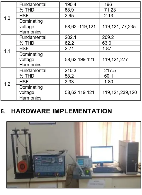
5429 1.1
Fundamental 202.1 209.2
% THD 62.2 63.9
HSF 2.71 1.87
Dominating voltage Harmonics
58,62,199,121 119,121,277
1.2
Fundamental 210.3 217.5
% THD 58.2 60.1
HSF 2.33 1.80
Dominating voltage Harmonics
58,62,119,121 119,121,239,120
5.
HARDWARE IMPLEMENTATION
Fig 10. Experimental Setup
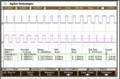
The methods were checked with the planned configuration consisting of a PWM inverter circuit based on FPGA. This requires an FPGA panel, a driver circuit inverter module, an autotransformer, and a motor drive induction. Yokogawa Digital Storage oscilloscope will be used for all the inverter output measurements. The experimental setup for control of an induction motor is shown in Figure 6.1 and the parameters required for the setup is listed in the Table 1.2. Using an autotransformer and a rectifier, the inverter is supplied with a 220 V DC voltage. FPGA has developed the traditional and proposed methods of PWM signals. Between the switches of the same inverter aid, a dead time of 2.9μ seconds is introduced to ensure a smooth transition in the switching states of the inverter shown in figure 11. The basic frequency of the inverter voltage was set at 50 Hz in accordance with the traditional and proposed schemes study. The modulation index ranges the 0.2 to 1.0, all hardware tests are evaluated. In the following section, software and hardware results of the specific methods are compared.
5.1 SINUSOIDAL PULSE WIDTH MODULATION Fixed switching frequency SPWM scheme is simulated in Simulink model and implemented by using FPGA based three phase inverter. The switching frequency of the fixed switching triangular frequency is 3 kHz. The harmonic spectral analysis of voltage waveform, output line voltage waveform, and output phase current waveforms and measurement window are revealed below from Figure 11 to 16
Parameters
0.1 Fundamental 18.02 18.11
% THD 388.4 393.0
HSF 15.33 14.01
Dominating voltage Harmonics
58,62 119,121
0.2 Fundamental 37.62 39.9
% THD 254.1 250.0
HSF 10.8 9.22
Dominating Voltage Harmonics 58,62,119, 121, 239,240 119,121, 239,360
0.3 Fundamental 58.19 60.13
% THD 194.29 197.8
HSF 7.80 7.18
Dominating voltage Harmonics
58,62,119, 121
119,121,239
0.4 Fundamental 77.21 79.4
% THD 161.8 164.3
HSF 6.57 5.19
Dominating voltage Harmonics
58,62,119, 121 ,178, 239
119,121, 239,120
0.5 Fundamental 95.02 100.4
% THD 139.9 138.2
HSF 5.67 4.9
Dominating voltage Harmonics
58,62,119, 121,177
119,120,239
0.6 Fundamental 113.5 116.6
% THD 121.9 125.0
HSF 4.93 4.36
Dominating voltage Harmonics 58,62,119, 121,177, 181 119,1, 120,359
0.7 Fundamental 134.3 137.8
% THD 104.0 106.6
HSF 4.19 3.6
Dominating voltage Harmonics
58,62,119, 121
0.8 Fundamental 152.6 157
% THD 90.9 92.12
HSF 3.63 3.0
Dominating voltage Harmonics
58,62, 119,121
119,121, 239,120 0.9 Fundamental 170 175.1
% THD 80.7 83.09
HSF 3.18 2.56
Dominating voltage Harmonics
58,62,119,1
5430
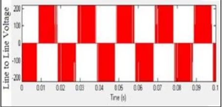
Fig 11. Simulation result of line to line voltage
Fig 12 Experimental result of line to line voltage with
current
Fig 13 Performance measurements, ma=0.8
Fig 14 PWM pulses with dead time, ma=0.8
Fig 15. Simulation Harmonic Spectrum for line to line voltage, ma=0.8
Fig 16. Experimental Harmonic Spectrum for line to line voltage, ma=0.8
Table 1.3 Simulation and Experimental Result comparison
Techni
que SPWM
Simulation Results Hardware results
ma Output Voltage
THD % T
HSF
Output
Voltage THD % HSF
0.1 18.02 388.4 15.33 17.54 69.34 2.895
0.2 37.62 254.1 10.86 36.5 60.67 3.545
0.3 58.19 194.29 7.80 57.21 53.68 4.155
0.4 77.21 161.84 6.57 74.6 45.81 4.765
0.5 95.02 139.95 5.67 94.10 36.89 5.045
0.6 113.5 121.97 4.93 112.5 30.21 5.355
0.7 134.3 104.05 4.19 133.4 27.53 5.415
0.8 152.6 90.94 3.63 151.2 24.01 5.465
0.9 170 80.70 3.18 168.2 21.43 5.186
1.0 190.4 68.99 2.95 186.6 18.66 4.465
1.1 202.1 62.28 2.71 200.9 16.96 4.274
5431 pulses are shown below from Figure 6.10 to 6.15.
Fig 17 Simulation result of line to line voltage
Fig 18. Experimental result of line to line voltage with current
Fig 19. Experimental measurements
Fig 20. Experimental RPWM Pulses
Fig 21 Simulation Harmonic Spectrum for line to line voltage, ma=0.8
Fig 22 Experimental results of Harmonic spectrum
Table 1.4 Simulation and Experimental Result comparison
Techni
que RPWM
Simulation Results Hardware results
M38.21 Outut Voltag e
THD
% HSF
Outp ut Voltage
THD
% HSF
0.1125.
06 18.11 393.0 7
14.0
1 25.43 71 3.843
0.2106.
67 39.99 250.5
6 9.22 40.2 61 3.275
0.3 60.13 197.8
6 7.18 67.65 56 3.945
0.4 79.46 164.3
9 5.91 78.3 47 4.435
0.5 100.4 6
138.2
1 4.99 99.2 41 4.534
0.6 116.6 125.0
6 4.36 120.5 32 4.755
0.7 137.8 106.6
7 3.62 142.3 28.3 4.643
0.8 157 92.12 3.00 163.04 22 4.535
0.9 175.1 83.09 2.56 141.8 19.7 4.10
1.0 196.8 71.23 2.13 185 17.2 3.805
1.1 209.2 63.97 1.87 200.4 16.3 3.691
5432
6.
CONCLUSION
Both sinusoidal PWM and two triangular random pulse width modulations are defined in the digital implementation of FPGA. There is talk of the comprehensive SPWM and FPGA's two triangle RPWM generation. In the MATLAB environment, the spectral analysis of the above methods is carefully investigated. Experimentation will examine the validity of the simulated spectral analysis. Comparisons demonstrated an outstanding equivalence between simulation and spectra that was actually measured. Two triangle random pulse width modulations outperform at the end of this study. But there is some scope to increase the fundamental by RPWM method if sine reference is replaced by space vector wave. The randomization also can be increased if the numbers of random carriers are increased.
7.
REFERENCE
[1] Amara, Fre`de`ric, Amiel& Thomas, ea 2006, ‘FPGA vs ASIC for low power applications’, microelectronicsJournal (Elsevier), vol .37, no .8, pp.669-677
[2] Amir,peyghambari, alidastfan&alireza, ahmadyfard 2015, ‘strategy for switching period selection in random pulse width modulation to shape the noise spectrum’, IET power electronic, vol. 8, no.4, pp. 517-523
[3] Bin Wu 2006,’High power converters and AC drives,’ New York: Wilcy-Interscience-IEEE Press [4] Bech, MM, Blaabjerg, F.Pedersen, JK
2000,’random modulation techniques with fixed switching frequencefor three-phase power converters ,’IEEE Transactions on Power Electronics, vol.15, no.4,pp753-761
[5] Gayathir, n &Chandorkar, MC 2008,’Design and implementation of FPGA based phase modulation control for series resonant inverter’,Sadhana, vol.33,no.5,pp. 505-522
[6] Bose, BK 2002, ‘Modern Power electronics and AC Drives’ , (E.L. PearsoED.) Upper Saddle River:prentice-Hall PTR
[7] Holtz, j 1992, “Pulse width Modulation – A survey”, IEEE Transactions on Industrial Electronics, vol. 39, no, 5, pp,410-420.
[8] G. Jegadeeswari, “Design and Implementation of THD Reduction for Cascaded Multilevel H-Bridge Inverter”Journal of Advanced Research in Dynamical and Control Systems (JARDCS), November 2017/Volume 11, Special Issue/Page no:(638-644)/ ISSN 1943-023X / Impact Factor: 3.514
[9] G. Jegadeeswari, “Design of SVPWM Inverter for Induction Motor Drive Using Neural Network Predictive Control”, International Journal for Research in Applied Science & Engineering Technology (IJRASET), April 2018/ Volume 6/ Issue IV /Page no (1007-1015) /ISSN: 2321-9653/ IC Value: 45.98/ SJ Impact Factor:7.076
[10]R. Zahira, D. Lakshmi C.N. Ravi and S. Sasikala, “Power Quality Enhancement Using Grid Connected PV Inverter”, Journal of Advanced Research in Dynamical & Control Systems, special issue, Vol 10, No 5. Jan 2018 pp 309-317. (Scopus Indexed).