Current Feedback Amplifier
Based Voltage Mode Multifunction Filter
SHEIKH AJAZ BASHIR *
Department Of Electronics & Instrumentation Technology, University Of Kashmir, Srinagar-190006
Kashmir , India
Email :[email protected] *corresponding author
N.A.SHAH
Department Of Electronics& Instrumentation Technology, University Of Kashmir, Srinagar-190006
Kashmir , India Email :[email protected]
F.A.KHANDAY
Department Of Electronics & Instrumentation Technology, University Of Kashmir, Srinagar-190006
Kashmir , India
Email :[email protected]
ABSTRACT
Here we propose a new Voltage – mode biquadratic three input and Single output (TISO) multifunction filter based on two current feedback amplifiers (CFAs) four resistors and two capacitors. This second order filter circuit is capable of realizing various filter functions by choosing values of the three inputs variably. The natural frequency (ω0)can be tuned with passive components and the Q of the circuit is independent of (ω0) .The higher cascading capability of the circuit is ensured because of its low - output impedance. Further PSPICE-simulated results are in conformity with theoretical values.
KEYWORDS
CFA ; Voltage Mode ;Biquad; Universal Filter
INTRODUCTION
Current mode circuits have been receiving considerable attention in analog signal processing and many application circuits have been reported in literature[1].A new circuit configuration called Current Feedback Amplifier (CFA) was developed to improve the finite gain-bandwidth product of the conventional voltage - feedback operational amplifier[2]. It can provide not only a constant bandwidth independent of closed loop gain but also a high slew – rate capability[3]. Usage of CFA as a basic building block in active filter design is highly beneficial on account of these factors.The applications and advantages in realizing active filter transfer functions using CFAs have received great attention because the amplifier enjoys the features of constant bandwidth independent of closed-loop gain and high slew rate, besides having low output impedance. Thus, it is advantageous to use CFA as a basic building block in the accomplishment of various analog signal processing tasks.
CFA can be represented symbolically as shown in Fig-1
FIG-1 Symbolic Representation of CFA
Further the CFA circuit is equivalent to a second generation current conveyor [7] with a voltage buffer [8].
Its characteristics can be modeled by the matrix
andresulting port relations for the CFA are
vx = vy,vo = vz, iy=0, and ix=iz ---(1)
According to the above set of port relations the CFA is constituted of a second generation current conveyor (CCII) followed by a voltage follower. Here we are talking about a non-inverting CFA while as ix= -iz indicates an inverting CFA . Further the non-inverting input (y)of a CFA connects to the input of a buffer and as such it has a very high impedance. The inverting input (x) connects to the input buffer’s output , so the inverting input impedance is quite low.
The output buffer provides low output impedance for the amplifier. The output impedance is modeled as a first order RC parallel combination. This output impedance in parallel with output buffer’s input impedance results in the parasitic high value impedance at the I-V conversion node, which is the compensating Z-terminal. These characteristics help in operating filtering topologies in different modes .
z x
y
z x y
v
i
v
i
v
i
0
1
0
0
0
1
0
0
0
When y-terminal of a CFA is used as an input and output achieved through the output buffer , the amplifier behaves ideally in voltage mode.
PROPOSED CIRCUIT
From routine Circuit analysis , the characteristic equation of the proposed CFA based VM Biquad circuit can be written as
--- (2)
The natural frequency of the circuit (ω0)will be as shown in equation (3) Here the value of (ω0) can be adjusted by changing the values of passive components R2 and R3 --- (3)
Further the Quality factor of the filter block will be derived from equation-(4) where its value will be independent of (ω0) and can be adjusted with variation in R4 only.
--- (4)
Realization of various filter topologies is possible by varying the inputs as under;
INPUT VALUES FILTER REALIZATION
V2 = V3 = 0 V1 = Vin A Second Order High Pass Filter
V2 = V3 = 0 V2 = Vin A Second Order Band Pass Filter
V1 = V2 = 0 V3 = Vin A Second Order Low Pass Filter
6 1 3 2 5 4 3 1 2 6 1 5 3 3 1 4 2 2 1
1
1
1
1
1
1
C
C
R
R
R
R
R
C
s
s
C
C
R
R
V
C
R
s
V
s
V
V
out
6 1 3 21
C
C
R
R
o
6 1 3 2 4 2 3 4 3 2 4C
C
R
R
R
R
R
R
R
R
R
Q
V2 = 0 V1 = V3 = Vin A Second Order Notch Filter
V1 = - V2 =V3 = Vin A Second Order All Pass Filter
CIRCUIT SIMULATION
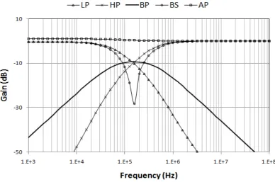
The performances of the proposed circuit given in Fig. 3 has been simulated with PSPICE program. In the simulations, the commercially available current feedback amplifiers(CFAs), i.e., AD844 of Analog Devices were used. The circuit was supplied with symmetrical voltages of ±15 V. The simulated frequency characteristics of all the filter functions of the proposed CFA-based VM multifunction Universal circuit in Fig. 3 are shown in Fig. 4 with the passive component values:R2 = R3 = R4= R5= 1 K Ohm , C1 = C6 = 1nF leading to fo = 159.15 KHz and Q = 1/3 (Gain for BP response at fo = 0.3) . The filter is designed for a natural angular frequency of fo= ωo/2π≅159.15 kHz and the quality factor of Q = 1/3 . With the same setting, the simulated
gain and phase responses of the AP filters verifying theory values are depicted in Figs. 5. From the figures, it appears that the simulation results are in excellent agreement with theoretical values.
Figure 4. Magnitude response of proposed CDBA based voltage mode multifunction filter with R2 = R3 = R4 = R5 = 1 Kohm, C1 = C6 = 1nF leading to fo = 159.15 KHz and Q = 1/3 (Gain for BP response at fo = 0.3).
Figure 5. Phase response of Allpass Response.
CONCLUSION
In this paper , a Universal biquadratic multifunction filter using two CFAs is introduced. The proposed circuit is able to realize Low Pass , High Pass , Band Pass , All Pass and Notch function as well. Besides employing two CFAs, there are four resistive and two reactive components in the circuit block. Further incase of proposed circuit Q is independent of (ω0)and can be varied by simply changing the value of R4 only. The tuning of filter i.e ; changing the value of (ω0) is possible by changing the value of passive components R2 and R3 in the circuit.
REFERENCES
[1] B.Wilson“Recent developments in current conveyors and current mode circuits,” IEE Proc.G,, vol. 137, no. 2, pp. 63–77, April 1990.
[2] Comlinear Corp., “Designer’s guide for 200 series Op amp”, Application note 200-1, 4800, wheaton Drive,Ft.collins, CO 80525, Nov.1984.
[3] Analog Devices:“Linear Products Data Book ” Norwood MA, 1990.
[4] R. Nawrocki and U .Klein ,, “New OTA-Capacitor realization of a universal biquad,” ElectronicsLetters, vol. 22, no. 2, pp. 50-51, 1986.
[5] C.Toumazou and F.J.Lidgey ,, “Universal active filter using current conveyors,” Electronic letters, vol. 22, pp. 662-664, 1986. [6] C.M.Chang and P.C.Chen,“Universal active filter with three inputs and one output using current conveyors ,” International J
Electron, vol. 71, n, pp. 817-819 1991.
[7] Sedar and K.C. Smith, “A second Generation current conveyor and its applications,” IEEE transactions circuit theory, vol. CT-17, pp. 132-134, 1970.