Design And Construction Of The Frequency Divider
Using 7490 Decade Counter
May Zaw Tun, Ei Ei Minn
Natural Science Department, University of Computer Studies (Mandalay), Myanmar
Natural Science Department, University of Computer Studies (Mandalay), Myanmar
Abstract: A frequency divider is a circuit that divides a giving frequency by a factor of n, where n is an integer. Clock frequency dividers generate slower clocks from a faster reference. A frequency divider circuit is a simple clock frequency divider circuit, designed with readily available electronic components. This circuit is based on TTL ICs. It consumes very low power in quiescent state. It consists of a 10MHz crystal oscillator, a hex inverter IC 7404, seven decade counter ICs 7490 and other electronic components. The heart of the frequency divider circuit is seven 7490 decade counters in cascade. Input frequency 10 MHz is reduced to 1Mz through 1Hz by using seven decade counter ICs.
Keywords: 7490 decade counter, 7404 hex inverter, 10 MHz crystal
1.
Introduction
Frequency dividers are widely considered as a major limiting factor in frequency synthesizer systems, which require a very fast settling frequency feedback loop and a wide-range of frequency division ratios. Among the most important parameters of high-speed dividers are the operating frequency, operating range, and power consumption. Most modern frequency dividers are typically classified as cascaded asynchronous programmable prescaler counters, programmable swallow counters, or programmable divide-by-N counters. The cascaded asynchronous programmable prescaler counter offers a high operating speed due to the absence of a long delay loop (the feedback delay is only present between adjacent cells). However, the operating frequency is degraded by the increase in the number of cascaded cells, which are usually controlled by a synchronous binary programmable value. Furthermore, these counters suffer from a large accumulated jitter due to a long asynchronous cascaded cell topology. The programmable swallow counter provides a wide variety of dividing ratios, which makes this counter amenable to multi-system applications. These counters are composed of an N-bit programmable counter, an S-bit swallow counter, and a P -bit prescaler counter, which results in an input frequency (Fin) to output frequency (Fout) relationship of Fout = (NP + S)Fin. The structure has a minimum division ratio of P2, meaning that it requires a delay of P2 cycles to produce the output pulse. Furthermore, the structure lacks modularity, which limits its flexibility and reusability of low-cost design cells. The divide-by-N frequency divider , also known as an integer- N divider, exploits a large wide-range division ratio which can vary from 2 to N where N is an arbitrary integer value less than 2M for an M-bit divider. Even though the division ratio is not as flexible as a programmable swallow counter and the operation is not as fast as an asynchronous prescaler divider, research has shown that the integer-N frequency divider is more practical in terms of design time, continued cost-effective technology scaling, and has low spurious sideband effects compared to a fractional-N (i.e. swallow and prescaler) frequency divider. [4, 6]
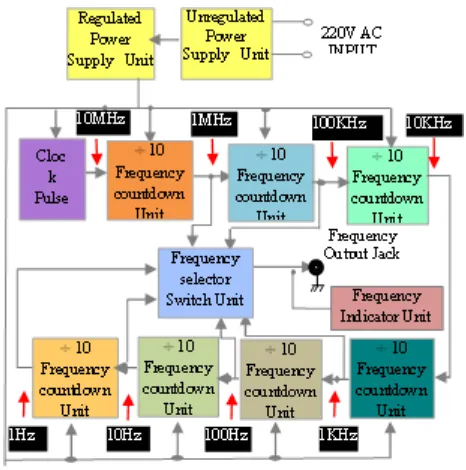
Figure 1.Block diagram of the frequency divider circuit.
All computers require a timing source to provide accurate clock waveforms. The timing section controls all system timing and is responsible for the proper operation of the system hardware. The timing action usually consists of a crystal controlled oscillator and counters for frequency division. Using a high frequency oscillator divided down to a lower frequency provides for greater accuracy and frequency stability. A digital counter uses for counting the number of times that a digital event has occurred. The frequency divider circuit is constructed with seven decade counters, a Hex inverter, a 10 MHz crystal and a few additional electronic components. The block diagram for this construction is shown in figure 1.
2. Background theory
2.1 Clock Signal
In electronics and especially synchronous digital circuits, a clock signal is a particular type of signal that oscillates between a high and a low state and is utilized like a metronome to coordinate actions of circuits. A clock signal is produced by a clock generator. Although more complex arrangements are used, the most common clock signal is in the form of a square wave with a 50% duty circle, usually with a fixed, constant frequency. [1] Circuits using the clock signal for synchronization may become active at either the rising edge, falling edge, or, in the case of double data rate, both in the rising and in the following edges of the clock cycle.
2.2 Clock Pulse Generator
A clock pulse generator is a circuit that produces a timing signal (known as a clock signal and behaves as such) for use in synchronizing a circuit’s operation. The signal can range from a simple symmetrical square wave to more complex arrangements. The basic parts that all clock generators share are a resonant circuit and an amplifier. The resonant circuit is usually a quartz piezo- electric oscillator, although simpler tank circuits and even RC circuits may be used. The amplifier circuit usually inverts the signal from the oscillator and feeds a portion back into the oscillator to maintain oscillation. The generator may have additional sections to modify the basic signal. Other such optional sections include frequency divider or clock multiplier sections. Programmable clock generators allow the number used in the divider or multiplier to be changed, allowing any of a wide variety of output frequencies to be selected without modifying the hardware.
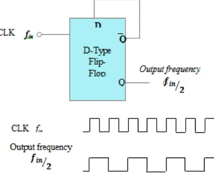
2.3 D-Type Flip-Flop Frequency Divider
The D-type Flip-Flop is as a binary divider, for frequency division or as a "divide-by-2" counter. D-type frequency divides by two circuit and corresponding input and output waveform is also shown in figure 2.
Figure 2. Divide by two frequency divider and corresponding input and output waveform
The D-type logic flip flop is a very versatile circuit. It can be used in many areas where an edge triggered circuit is needed. In one application this logic or digital circuit provides a very easy method of dividing an incoming pulse train by a factor of two. The divide by two circuits employs one logic d-type element. Simply by entering the
pulse train into the clock circuit, and connecting the Q output to the D input, the output can then be taken from the Q connection on the D-type . The circuit operates in a simple way. The incoming pulse train acts as a clock for the device, and the data that is on the D input is then clocked through to the output. Take the situation when the Q output is a level '1'. This means that the Q output will be at '0'. This data is clocked through to the output Q on the next positive going edge from the incoming pulse train on the clock input. At this point the output changes from a '1' to a '0'. At the next positive going clock pulse, the data on the Q output is again clocked through.
2.4 Toggle Mode Flip-Flop Frequency Divider
For frequency division, toggle mode flip-flops are used in a chain as a divide by two counters. One flip-flop will divide the clock, ƒin by 2, two flip-flops will divide ƒin by 4 (and so on). A toggle flip-flop has two states, the "toggle state" and the "memory state". Since there are only two states, a T-type flip-flop is ideal for use in frequency division and counter design. Frequency division using Toggle flip-flops is shown in figure 3.
Figure 3. Frequency division using Toggle Flip-flops
Binary ripple counters can be built using "Toggle" or "T-type flip-flops" by connecting the output of one to the clock input of the next. Toggle flip-flops are ideal for building ripple counters as it toggles from one state to the next, (High to Low or Low to High) at every clock cycle so simple frequency divider and ripple counter circuits can easily be constructed using standard T-type flip-flop circuits. If we connect together in series, two T-type flip-flops the initial input frequency will be "divided-by-two" by the first flip-flop ( f÷2 ) and then "divided-by-two" again by the second flip-flop ( f÷2 )÷2, giving an output frequency which has effectively been divided four times, then its output frequency becomes one quarter value (25%) of the original clock frequency, ( f÷4 ). [2] Each time we add another toggle or "T-type" flip-flop the output clock frequency is halved or divided-by-2 again and so on, giving an output frequency of 2nwhere "n" is the number of flip-flops used in the sequence. Then the Toggle or T-type flip-flop is an edge triggered divide-by-2 device based upon the standard JK-type flip flop and which is triggered on the rising edge of the clock signal.
for frequency division is commonly known as an
Asynchronous 3-bit Binary Counter as the output on QA to QC, which is 3 bits wide, is a binary count from 0 to 7 for each clock pulse. In an asynchronous counter, the clock is applied only to the first stage with the output of one flop stage providing the clocking signal for the next flip-flop stage and subsequent.
3.
Hardware Description
The circuit is constructed by using BCD counter (74LS90) and Inverter (7404).
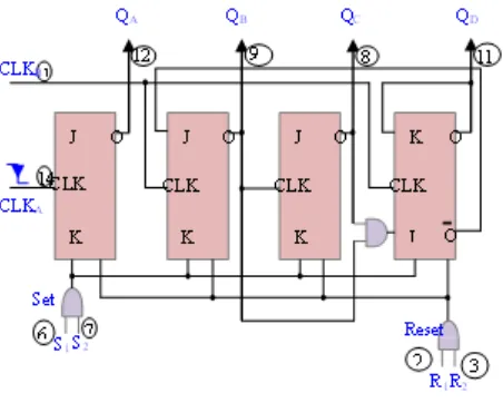
3.1 The 74LS90 BCD Counter
The 74LS90 integrated circuit is basically a MOD-10 decade counter that produces a BCD output code. The 74LS90 consists of four master-slave JK flip-flops internally connected to provide a MOD-2 (count-to-2) counter and a MOD-5 (count-to-5) counter. The 74LS90 has one independent toggle JK flip-flop driven by the CLK A input and three toggle JK flip-flops that form an asynchronous counter driven by the CLK B input as shown in figure 4. The counters four outputs are designated by the letter symbol Q with a numeric subscript equal to the binary weight of the corresponding bit in the BCD counter circuits code. The 74LS90 counting sequence is triggered on the negative going edge of the clock signal, that is when the clock signal CLK goes from logic 1 (HIGH) to logic 0 (LOW). [5]
Figure 4.SN 74LS90 BCD counter
The additional input pins R1 and R2 are counter “reset” pins while inputs S1 and S2 are “set” pins. When connected to logic 1, the Reset inputs R1 and R2 reset the counter back to zero, 0 (0000), and when the Set inputs S1 and S2 are connected to logic 1, they Set the counter to maximum, or 9 (1001) regardless of the actual count number or position. The 74LS90 counter consists of a divide-by-2 counter and a divide-by-5 counter within the same package. Then we can use either counter to produce a divide-by-2 frequency counter only, a divide-by-5 frequency counter only or the two together to produce our desired divide-by-10 BCD counter.
3.2 The Hex Inverter IC 7404
The TTL 7404 device is shown in Figure 5. This
chip is called a hex inverter because it contains six
independent TTL inverters. The positive side of the
+5 V power supply is applied to pin no. 14, while the
ground side is applied to pin no.7. Although by no
means universal, this pinout configuration for the
power terminals is very common in digital IC
devices. There is no interaction between the inverter
sections, so all six may be used independently. The
average current drain is 12 to 15 mA. [5]
Figure 5. Pin connection diagram of a Hex inverter IC 7404
4. Operation of the Frequency Divider
Circuit
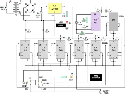
consisting of IC2 (7404). This clock pulse is fed to pin1 of
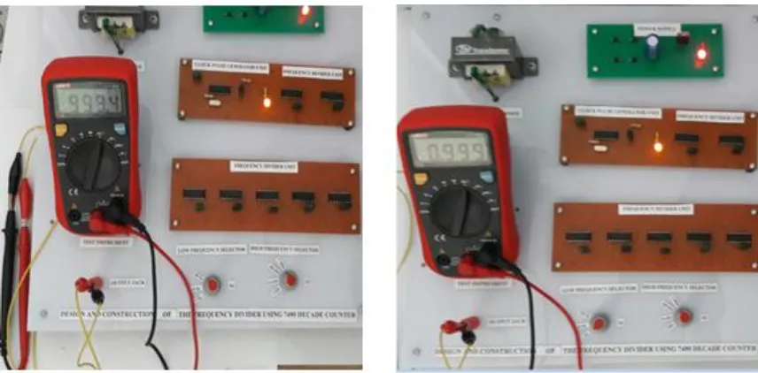
IC3 (IC 7490), which divides it by 10 to give a 1 MHz clock pulse at its output pin12. The 1 MHz clock pulse is fed to the input of the next stage and so on up to IC9. Thus at all the seven counter stages, we get unique output pulses (1MHz, 100 kHz, 10 kHz, 1 kHz, 100 Hz, 10 Hz and 1 Hz, respectively). These output pulses are selected by rotary switches S1, S2 and fed to an output jack as shown in figure 7. The blinking/flash rate of LED2 indicates the output frequency. However, you can identify output frequencies of 1 Hz and 10 Hz only.
Table 1.Output data measurement of the frequency divider circuit
Above 10 Hz, the LED blinks so fast that it’s not possible to estimate the frequency. Output data measurement of this frequency divider circuit is described in Table 1.
Figure 6. Schematic diagram of the Frequency Divider Using 7490 ICs
Frequency Range
Output Frequency (experimental results)
Frequency Difference
Percent of Error
1 MHz 999.4 kHz 0.6 kHz 0.06%
100 kHz 99.95 kHz 0.05kHz 0.05%
10 kHz 9.995 kHz 0.005 kHz 0.05%
1 kHz 999.5 Hz 0.05 Hz 0.05%
100 Hz 99.94 Hz 0.06 Hz 0.06%
10 Hz 9.995 Hz 0.005 Hz 0.05%
Figure 7. Photograph of the Frequency Divider using 7490 ICs
5. Results and Conclusion
In this report, the frequency divider circuit was constructed with locally available electronic components. This frequency divider circuit was designed to divide the frequency of a TTL compatible square wave signal which can be programmed with the use of seven 7490 to perform the required operation. This circuit can be built with a hex inverter IC 7404, seven decade counter IC 7490 and a few additional parts. The clock pulse generator unit of this frequency divider circuit was used 7404 IC as oscillator mode. The output frequency of clock pulse generator circuit is 10 MHz. Seven decade counter ICs CD7490 counts the pulses generated by the 7404 and gives the corresponding BCD outputs. We conclude that the constructed frequency divider circuit may be used in a number of electronic applications such as fax or modem interface used in a personal computer system that is capable of selecting a large number of clock frequencies for driving internal Universal Asynchronous Receiver/Transmitter (UART). In all the applications related to this circuit, the most important feature that they offer is digital timing and frequency division since they are easily cascadable giving limitless possibilities to timing delays. Device parameters and new design techniques can be found on the basis of this various circuit design based on this paper report to study the various fields.
References
[1] M. Zhang, S.K. Islam, M.R. Haider, A fast programmable frequency divider with a wide dividing-ratio range and 50% duty-cycle. IEICE Electron. Express 4(21), 672–678 (2007)
[2] Chi-Sheng Lin, Ting-Hsu Chien, Chin-Long Wey. A 5.5-GHz 1-mW Full-Modulus-Range Programmable Frequency Divider in 90-nm CMOS Process, IEEE Transactions on Circuits and Systems II, 58(9), p.550-554, (2011).
[3] IC Frequency Dividers & Counters, January 1969 Electronics World, By Donald L. Steinbach Research Engineer Lockaheed Missiles and Space Co.
[4] R. Shankar and A. S. Leno, N+1 frequency divider counter and method therefore, US Patent 5,526,391, June 1996.
[5] Don Lancaster, CMOS Cookbook (Indianapolis, IN: Howard Sams, 1977) and TTL Cookbook (Indianapolis, IN: Howard Sams, 1974.