and substrate loss in the wideband regime, which cannot be accurately described by the conventional -model. Good match with the measuredS-parameters, ( ), Re( in( )), and ( ) proves the proposed T-model. Besides the broadband feature, scalability has been justified by good match with a linear function of coil numbers for all model parameters employed in the RLC networks. The satisfactory scalability manifest themselves phys-ical parameters rather than curve fitting. A parameter extraction flow is established through equivalent circuit analysis to enable automatic parameter extraction and optimization. This scalable inductor model will facilitate optimization design of on-chip inductor and the accuracy proven up to 20 GHz can improve RF circuit simulation accuracy demanded by broadband design.
Index Terms—Broadband, inductor, lossy substrate, scalable.
I. INTRODUCTION
T
HE LACK of an accurate and scalable model for on-chip inductors becomes one of the most challenging problems for Si-based RF integrated circuit (IC) design. The existing models suffer two major drawbacks in terms of accuracy for limited bandwidth and poor scalability. Many publications reported improvement on the commonly adopted -model by modification on the equivalent circuit scheme [1]–[3]. How-ever, limited bandwidth to few gigahertz remains an issue for most of the modified -models. A two- model was proposed to improve the accuracy of and beyond self-reso-nance frequency [4]. Unfortunately, this two- model suffers a singular point above resonance [5]. Besides, the complicated circuit topology with double element number will lead to difficulty in parameter extraction and greater time consumption in circuit simulation [6]. Recent work using modified T-model demonstrated promising improvement in broadband accuracy and suggested the advantage of T-model over -model [7]. However, the scalability of model’s major concern was not reported. In our paper, a T-model of new circuit scheme is pro-posed to realize two primary features, i.e., broadband accuracy and scalability. Our T-model is composed of twoRLCnetworksManuscript received September 8, 2005; revised December 2, 2005. This work was supported in part by the National Science Council of Taiwan, R.O.C. under Grant 93-2220-E009-018 and Grant 94-2220-E009-018.
The authors are with the Department of Electronics Engineering, Na-tional Chiao-Tung University, Hsinchu 300, Taiwan, R.O.C. (e-mail: [email protected]).
Digital Object Identifier 10.1109/TED.2005.864409
other four elements, , , and are employed to account for the lossy substrate. allocated between two RLC networks is responsible for coupling between two networks, i.e., the spiral inductor and lossy substrate. All the physical elements are constants independent of frequencies and can be expressed by a close form derived from circuit analysis on the proposed T-model. Parameter extraction and optimization can be conducted with an initial guess extracted by approximation valid for specified frequency range. All the model parameters manifest themselves with predictable scalability w.r.t. coil numbers and physical nature. A parameter extraction flow has been established to enable automatic pa-rameter extraction and optimization that is easy to be adopted by existing circuit simulators like Agilent ADS or parameter extractor such as Agilent IC-Cap. The model accuracy over broadband is validated by good agreement with the measured
S-parameters, , Re , and up to 20 GHz
(Re is the real part of input impedance). It is expected that this scalable inductor model can effectively improve RF circuit simulation accuracy in broad bandwidth and facilitate the design optimization using on-chip inductors.
II. TECHNOLOGYAND CHARACTERIZATION
Spiral inductors of square coils were fabricated by 0.13 m back end technology with eight layers of Cu and low-k inter-metal dielectric ). The top metal of 3 m Cu was used to implement the spiral coils of width fixed at 15 m and inter-coil space at 2 m. The inner radius is 60 m and outer radius is determined by different coil numbers 2.5, 3.5, 4.5, and 5.5 for this paper. The physical inductance achieved at sufficiently low frequency are around 1.96 8.66 nH corresponding to coil numbers .S-parameters were measured by using Agilent network analyzer up to 20 GHz and de-embedding was carefully done to extract the truly intrinsic characteristics for model parameter extraction and scalable model build up.
III. T-MODEL’SEQUIVALENT CIRCUIT ANDMODEL
PARAMETEREXTRACTIONFLOW
A. T-Model Equivalent Circuit Schematics and Analysis
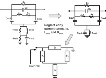
Fig. 1(a) illustrates the circuit schematics of the proposed T-model for on-chip inductors in which twoRLCnetworks of four physical elements for each part are linked through to
414 IEEE TRANSACTIONS ON ELECTRON DEVICES, VOL. 53, NO. 3, MARCH 2006
Fig. 1. T-model for on-chip spiral inductors. (a) Equivalent circuit schematics. (b) Intermediate stage of schematic block diagrams for circuit analysis. (c) Final stage of schematic block diagrams for circuit analysis.
account for the coupling between the spiral inductors and lossy substrate underneath. The physical property is defined for each element in the equivalent circuit. and represent the spiral metal coil’s series resistance and inductance respectively. is a new parameter created in our model to account for spiral coil’s conductor loss originated from lossy substrate return path.
indicates the inter-coil and under-pass capacitance and accounts for the spiral coil to substrate coupling capacitance.
and represent the lossy substrate resistance and ca-pacitance. and are two more new elements created in our model to describe the eddy current induced substrate loss. accounts for the reactive power loss crossing the substrate and is responsible for the resistive loss or joule heat dis-sipation. Fig. 1(b) indicates the schematic block diagrams de-rived by circuit analysis theory to extract the physical circuit elements as proposed. represents theRLCnetwork for spiral inductor and is another one representing lossy substrate.
acts as the coupling path between and . The circuit scheme is further transformed to Fig. 1(c) to correlate withY-parameters from 2-port measurement.
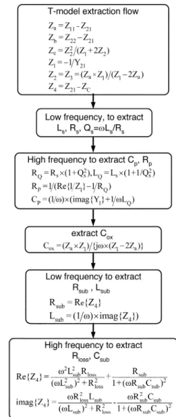
B. Model Parameter Extraction and Optimization Principle
All the unknownR, L, Cparameters are extracted from an-alytical equations derived from equivalent circuit analysis as shown in Fig. 1. The analytical equations are composed of Z -and/orY-parameters listed in the first block of extraction flow illustrated in Fig. 2, which can be easily transformed from the measured S-parameter after appropriate de-embedding. Under the condition that the number of unknown elements is larger than the number of equations (for most of complicated problems like this one), the approximation valid under very low or very high frequency is generally made to remove some unknown el-ements and extract the remaining ones as the first step, and then to extract the others at the second step. Due to the necessary ap-proximation, the extractedR,L,Cparameters in the first run of flow (Fig. 2) are generally not the exactly correct solutions but just serve as the initial guess for further optimization through best fitting to the measuredS-parameters, , Re ,
and .
Fig. 2. T-model parameter formulas and extraction flow chart.
C. T-Model Parameter Extraction Flow and Physical Properties
As a result, all the physical elements composing the model can be extracted through the flow shown in Fig. 2. At the first step, and representing the physical inductor under very low frequency can be extracted. The ideal quality factor free from conductor and substrate losses, denoted as is given
by . After that, and can be extracted
by close forms as a function of ( , , ) and measured . represents the inter-coil and underpass cou-pling capacitance, which is one of major elements to determine the frequency response, particularly the correct self-resonance frequency and the phase near resonance. is a new element introduced in our study to model the spiral conductor loss and Q degradation before resonance . Eddy cur-rent in the coil metal arising from the magnetic field generated through substrate return path under high frequency is proposed as the origin responsible for the additional spiral conductor loss represented by [8]. is one more major element besides to determine self-resonance frequency and can be de-rived by the equation of Z-parameters shown in the flow chart.
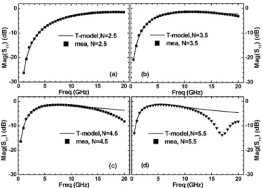
Fig. 3. Comparison of S (magnitude) between T-model simulation and measurement for spiral inductors. Coil numbers (a)N = 2:5, (b)N = 3:5, (c)N = 4:5, and (d)N = 5:5.
Then, and can be extracted easily from under very low frequency provided that and are relatively high impedances compared to and and can be ap-proximated as an open path. To the end, and can be extracted by the formulas shown in the last stage of flow chart based on all the known parameters and measured . is generally used to account for substrate resistance and the associ-ated energy loss. is another new element introduced in our T-model to simulate the eddy current generated on the Si sub-strate, which is expected in opposite direction against the current flow in the spiral coils according to the Lenz’ law. is re-quired to accurately model frequency response of L and Re near resonance but its effect on peak Q is negligible. On the other hand, has quite obvious effect on Q degradation over wide band. , , and are required simultaneously to describe the substrate loss precisely in terms of , , Re , and phase angle at different frequencies. has been generally used in conventional -model and it is justified as necessary for T-model to account for the degradation of and Q. is the last one in total 3 new elements ( , , and ) introduced in our T-model. plays its role ap-parent near or beyond resonance. Lack of will leave alone and lead to abnormal double hump in S-parameters, , and Re beyond resonance.
IV. BROADBANDACCURACY ANDSCALABILITY OFMODEL
A. Broadband Accuracy
The proposed T-model has been extensively verified by com-parison with measurement in terms of S-parameters ( , ), , Re , and over broad bandwidth up to 20 GHz. The scalability is validated by various geometries with split of coil numbers, 2.5, 3.5, 4.5, and 5.5. Broadband ac-curacy is justified by good match with measurement in terms of the mentioned key performance parameters. Fig. 3(a)–(d) indi-cates the comparison for magnitude of (Mag between the T-model and measurement. Excellent match is achieved for all coil numbers before resonance and agreement of curvature is maintained beyond resonance, which happened at
Fig. 4. Comparison of S (phase) between T-model simulation and measurement for spiral inductors. Coil numbers (a)N = 2:5, (b)N = 3:5, (c)N = 4:5, and (d)N = 5:5.
Fig. 5. Comparison of S (magnitude) between T-model simulation and measurement for spiral inductors. Coil numbers (a)N = 2:5, (b)N = 3:5, (c)N = 4:5, and (d)N = 5:5.
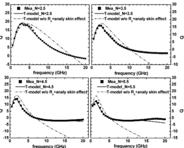
( : self-resonance frequency) for larger coil numbers ( and 5.5). Fig. 4(a)–(d) shows the good agreement in terms of in which precise match of resonance frequency is demonstrated for all coil num-bers. Fig. 5(a)–(d) reveals the exact match of Mag for smaller coils ( , 3.5) over full frequency range up to 20 GHz, which is well beyond resonance. Regarding the devi-ation beyond resonance for larger coils ( , 5.5) with , 5.1 GHz, i.e., far below 20 GHz, it happened to be a common issue suffered by EM simulation and will de-serve more study. Fortunately, this deviation did not make ef-fect on the accuracy of , Re , and beyond resonance. Again, Fig. 6(a)–(d) confirms the model accuracy in terms of over broadband beyond resonance for each coil number.
More extensive verification has been done by comparison of four key performance parameters for spiral inductors, i.e.,
, Re , , and . is the imaginary
part of input impedance , i.e., Im while Re represents the real part of .
416 IEEE TRANSACTIONS ON ELECTRON DEVICES, VOL. 53, NO. 3, MARCH 2006
Fig. 6. Comparison of S (phase) between T-model simulation and measurement for spiral inductors. Coil numbers (a)N = 2:5, (b)N = 3:5, (c)N = 4:5, and (d)N = 5:5.
Fig. 7. Comparison ofL(!)between T-model simulation and measurement for spiral inductor with various coil numbers (a)N = 2:5, (b)N = 3:5, (c)
N = 4:5, and (d)N = 5:5.
is the quality factor defined by Re . All three parameters are frequency dependent that is critically related to the spiral conductor loss and Si substrate loss. In fact, accurate simulation to predict , Re , and is the major goal of inductor models for circuit design and EM simulators for physical element design. In our study, the proposed T-model can provide very good match with the measurement for all the three parameters as follows. Fig. 7(a)–(d) illustrates the excellent fit to the measured by our T-model for all spiral inductors operating up to 20 GHz. The transition from inductive to capacitive mode evoked by increasing frequency beyond is accurately reproduced by the model. Regarding Re , pretty good match between the T-model and measurement is shown in Fig. 8(a)–(d). The T-model can exactly capture the full band behavior of Re even beyond resonance such as the dramatic increase prior to resonance, peak at resonance, and then sharp drop after the peak. Eventually, is of the primary concern for inductor design and the first key parameter governing RF IC performance such as power, gain, and noise
Fig. 8. Comparison of Re(Z (!)) between T-model simulation and measurement for spiral inductors with various coil numbers (a)N = 2:5, (b)
N = 3:5, (c)N = 4:5, and (d)N = 5:5.
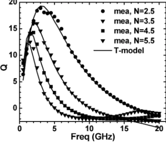
Fig. 9. Comparison ofQ(!)between T-model simulation and measurement for spiral inductor with various coil numbers:N =2.5, 3.5, 4.5, and 5.5.
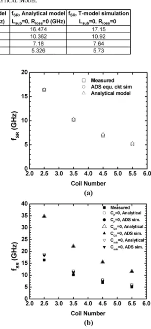
figure, etc. Fig. 9 reveals the excellent match with the measured over the broad bandwidth of 20 GHz. The exact fit to the peak Q and capture of full band behavior for all coil numbers suggests the advantage of our T-model compared to the existing -model. Self-resonance frequency is a key parameter accompanying with to quantify the useful bandwidth. In our T-model, can be accurately predicted by both full equivalent circuit simulation and analytical model of closed form given by (1). The analytical model is readily derived by equivalent circuit analysis on this new T-model and a simple formulas by closed form expressed as (1) is derived under appropriate approximation. The details of model equation derivation can be referred to the Appendix. The ap-proximation made by removing and was justified by impedance analysis and equivalent circuit simulation. Fig. 10 presents calculated by reduced T-model without and and the comparison with original T-model with and .The major difference is revealed in higher frequency region beyond the peak Q but the intercept point corresponding to , i.e., is nearly identical to each other. Table I lists the exact values of for comparison among measurement,
Fig. 10. Comparison of Q(!) and self-resonance frequency f corresponding to Q = 0 among T-model, reduced T-model (L =
R = 0)and measurement for spiral inductors with various coil numbers.
simulation by original T-model and reduced T-model, and calculation by analytical model of (1). The good agreement to each other in terms of deviation below 0.2 GHz justifies the approximation for reduced T-model and the derived analytical model for . The accuracy of calculated by the equiva-lent circuit simulation and analytical model is further validated by good match with the measured results shown in Fig. 11(a) for various coil numbers. Regarding the parasitic capacitance effect on as mentioned previously, Fig. 11(b) indicates the , , and effect on predicted by ADS simulation using full equivalent circuit and analytical model given by (1). The results from ADS simulation and analytical model show very good consistency. We see that the elimination of or can help to increase by around 15 20% cor-responding to , 3.5, 4.5, 5.5 while the elimination of can dramatically boost by more than 100%, i.e., more than double the existing performance for all coil numbers. The prediction from our T-model suggests that plays a dom-inant role in determining and spiral inductor on package is a potential solution to minimize and achieve maximum . Recently, low temperature co-fire ceramic (LTCC) has been promoted as a useful process to implement the RF passive elements on package wherein effective enhancement of Q and
has been demonstrated [9], [10]
(1)
Fig. 11. Self-resonance frequency f of on-chip spiral inductors with various coil numbers, N = 2:5, 3.5, 4.5, 5.5 (a) comparison between measurement, ADS simulation, and analytical model (b)C ,C , andC effect onf calculated by ADS simulation and analytical model. Comparison with measuredf to indicate thef increase contributed by eliminating the parasitic capacitances,C ,C , andC respectively.
B. Skin Effect–Frequency Dependent in Conventional Model and Constant in T-Model for Broadband Accuracy
Regarding the skin and current crowding effects, which are considered playing an important role on Q, a frequency depen-dent is generally proposed to fit the frequency response of Q over wide band. Through our study, the frequency dependent , i.e., formulated by the ideal model given by (2) is adopted and implemented to our T-model in which was removed to manifest effect alone. The simulated shown in Fig. 12 reveals obvious deviation from measured one over frequencies beyond that of peak Q and suggests that alone cannot simulate the frequency response accurately even
418 IEEE TRANSACTIONS ON ELECTRON DEVICES, VOL. 53, NO. 3, MARCH 2006
Fig. 12. Q(!)calculated by equivalent circuit removingR from original T-model and addingR (!)to simulate skin effect for spiral inductors with various coil numbers (a)N = 2:5, (b)N = 3:5, (c)N = 4:5, and (d)N =
5:5.
Fig. 13. Frequency dependent R extracted from measurement through definition of R (!) = Re(0=Y ) and the comparison with R (!) calculated by ideal model of (2) for spiral inductors with various coil numbers,
N =2.5, 3.5, 4.5, and 5.5.
in narrow band around the peak Q. Besides, the frequency de-pendent elements are generally difficult to be implemented in time-domain simulators such as SPICE [11]. To verify the origin responsible for the deviation, calculated by ideal model (2) is compared with the measured Re . The result shown in Fig. 13 indicates that the ideal model can accu-rately fit at very low frequencies GHz) but over-es-timates at frequencies beyond 2 GHz for all inductors of different coil numbers. The roll-off of revealed at higher frequency is proposed to stem from lateral substrate coupling ef-fect [6]. It is very interesting to note that the dramatic increase of predicted by skin-effect model at higher frequency is actually an over-estimation compared to the measured one but cannot help to accurately reproduce Q degradation at frequen-cies near or beyond the peak Q. In our T-model, has been
Fig. 14. L(!)calculated by equivalent circuit simulation withR removed from original T-model for spiral inductors with various coil numbers (a)N =
2:5, (b)N = 3:5, (c)N = 4:5, and (d)N = 5:5.
Fig. 15. Re(Z (!)) calculated by equivalent circuit simulation withR removed from original T-model for spiral inductors with various coil numbers (a)N = 2:5, (b)N = 3:5, (c)N = 4:5, and (d)N = 5:5.
introduced as a new element to account for the spiral conductor loss and Q degradation over wide band. To justify the role played by , simulation was done by removing from the original T-model to verify the impact on , Re , and as shown in Figs. 14, 15, and 16 respectively. We see that in this model has obvious effect on and Re at high frequency near resonance and significant impact on Q over wide band The physical property and origin as defined previously for , i.e., eddy current in the coil metal arising from the mag-netic field generated through substrate return path is believed an appropriate mechanism to account for the broadband character-istics in terms of , Re , and as demonstrated
Fig. 16. Q(!)calculated by equivalent circuit simulation withR removed from original T-model for spiral inductors with various coil numbers (a)N =
2:5, (b)N = 3:5, (c)N = 4:5, and (d)N = 5:5.
Fig. 17. T-model RLC network parameters versus coil numbers, spiral coil’s RLC network parameters (a)L , (b)R , (c)C andC , and (d)R .
whereL,W,andtare the metal line length, width, and thickness, respectively. is the conductivity, is the permeability, and
represents the skin depth of frequency dependence.
C. Model Scalability
Besides the broadband accuracy as presented, another impor-tant feature realized by this T-model is the good scalability w.r.t. geometry for all model parameters. Fig. 17 reveals good match with a linear function of coil numbers for each model param-eter in the spiral coil’sRLCnetwork, i.e., , , , , and . All five elements present monotonically increasing func-tion of coil number in which coefficient of first order derivative has been extracted for every parameter. In reality, the induc-tanceLfollows a curve more complicated than linear function. As shown in Fig. 17(a),Lcan be precisely fitted by a parabolic function ofN(coil number). Fig. 18 indicates the excellent fit by linear function for substrateRLCnetwork involved model pa-rameters, , , , and . The decrease of or increase of corresponding to larger coil number ac-counts for the worse substrate loss caused by increasing spiral coil size. Regarding , , and , all three terms follow linearly increasing function ofN. The scaling behavior revealed by the four parameters is physically derivable and sufficiently
Fig. 18. T-model RLC network parameters versus coil number, lossy substrate RLC network parameters (a)C , (b)1=R , (c)L , and (d)R .
Fig. 19. Equivalent circuit schematics and analysis of reduce T-model to derive the analytical model for calculating self-resonance frequencyf
accurate to calculate substrate loss effect on , , and , etc. for inductor of various spiral coil sizes. Regarding in-terest in more extensive scope of layout geometries such as coil metal width or inner radius, a preliminary work has been done to validate the model over wide range of widths (3, 9, 15, and 30 m). Good fit to all measured parameters as mentioned can be maintained and model scalability is presented as a parabolic function instead of a linear function. A minor modification to the original T-model by adding an inductor element in se-ries with to account for proximity effect can further improve the fitting accuracy. The detail will not be covered by this paper due to limited pages. The promisingly good scalability proven for full set of model parameters as demonstrated suggests that this T-model is useful in pre-layout simulation and optimization for physical design. The nature of easy link with standard circuit simulator makes this T-model useful in circuit element tuning and optimization for RF circuit design.
V. CONCLUSION
A broadband and scalable T-model has been developed to accu-rately simulate on-chip spiral inductors operating up to 20 GHz.
420 IEEE TRANSACTIONS ON ELECTRON DEVICES, VOL. 53, NO. 3, MARCH 2006
under the approximation (A7), (A8), (A9)
(A10)
(A11)
(A12)
A parameter extraction flow has been established through equiva-lent circuit analysis to enable automatic parameter extraction and optimization. Good scalability is validated for all model parame-ters and manifests the physical property underlying each param-eter. The results suggest that the proposed T-model can facilitate Si CMOS based RF IC design adopting on-chip inductors.
APPENDIX
The analytical model equation for calculating self-resonance frequency, is derived based on reduced T-model equivalent circuit analysis as shown in Fig. 19 and mathematical formulas development as follows: (A1) (A2) (A3) Re (A4) Im (A5) (A6) (A7) (A8) (A9) ACKNOWLEDGMENT
The authors would like to thank the Chip Implementation Center for ECAD tool support.
REFERENCES
[1] C. P. Yue and S. S. Wong, “Physical modeling of spiral inductors on silicon,”IEEE Trans. Electron Devices, vol. 47, no. 4, pp. 560–568, Apr. 2000.
[2] M. Park, S. Lee, C. S. Kim, H. K. Yu, and K. S. Nam, “The detailed analysis of high Q CMOS-compatible microwave spiral inductors in sil-icon technology,”IEEE Trans. Electron Devices, vol. 45, no. 10, pp. 1953–1959, Oct. 1998.
[3] P. Arcioni, R. Castello, G. D. Astis, E. Sacchi, and F. S. Svelto, “Mea-surement and modeling of Si integrated inductors,”IEEE Trans. Instrum. Meas., vol. 47, no. 11, pp. 1372–1378, Nov. 1998.
[4] Y. Cao, R. A. Grove, X. Huang, N. D. Zamdmer, J.-O. Plouchart, R. A. Wachnik, T.-J. King, and C. Hu, “Frequency-independent equivalent-circuit model for on-chip spiral inductors,”IEEE J. Solid-State Circuits, vol. 38, no. 5, pp. 419–426, May 2003.
[5] M. Fujishima and J. Kino, “Accurate subcircuit model of an on-chip inductor with a new substrate network,” inVLSI Symp. Tech. Dig., 2004, pp. 376–379.
[6] J. Gil and H. Shin, “A simple wide-band on-chip inductor model for silicon-based RF Ics,”IEEE Trans. Microw. Theory Techn., vol. 51, no. 12, pp. 2023–2028, Dec. 2003.
Jyh-Chyurn Guo received the B.S.E.E. and M.S.E.E. degrees from National Tsing-Hua Univer-sity (NTHU), Taiwan, R.O.C., in 1982 and 1984, respectively, and the Ph.D. degree in electronics en-gineering from the National Chiao-Tung University (NCTU), Hsinchu, Taiwan, in 1994.
Previously, she was working in the semicon-ductor industry with a focus on device design and VLSI technology development. In 1984, she joined the ERSO/ITRI, where she was engaged in semiconductor integrated circuit technologies with a broad scope to cover the high-voltage, high-power, submicron project, and high-speed SRAM technologies, etc. From 1994 to 1998, she was with Macronix International Corporation, where she was engaged in high-density and low-power flash memory technology development. In 1998, she joined Vanguard International Semiconductor Corporation, where she served as a Department Manager, responsible for advanced DRAM device technology development. In 2000, she joined Taiwan Semiconductor Manufacturing Company (TSMC), Hsinchu, where she served as a Program Manager in charge of 0.1-m logic CMOS FEOL, high-performance-analog and RF CMOS technology development. She joined NCTU in 2003 as an Associate Professor in the Department of Electronics Engineering. Her current research interests cover RF CMOS and high-performance analog device design and modeling, novel nonvolatile memory technology, and circuit technology for SOC. She has authored or co-authored more than 40 technical papers and has been granted 12 international patents in her professional field.