1 All Rights Reserved © 2012 IJARCSEE
HDL- Based Embedded Multiprocessor
Architecture
Mr.Sumedh S.Jadhav, Prof. C.N.Bhoyar
Abstract— Embedded multiprocessor design presents challenges and opportunities that stem from task coarse granularity and the large number of inputs and outputs for each task. We have therefore designed a new architecture called embedded concurrent computing (ECC), which is implement on FPGA chip using VHDL. The performances of a realistic application show scalable speedups comparable to that of the simulation. The design methodology is expected to allow scalable embedded multiprocessors for system expansion. In recent decades, two forces have driven the increase of the processor performance: Advances in very large-scale integration (VLSI) technology and Micro architectural enhancements. Therefore, we aim to design the full architecture of an embedded processor for realistic to perform arithmetic, logical, shifting and branching operations. We will be synthesize and evaluated the embedded system based on Xilinx environment. Processor performance is going to be improving through clock speed increases and the clock speed increases and the exploitation of instruction- level parallelism. We synthesized and evaluated the embedded system based on an Modelsim environment.
Index Terms—Multiprocessor design; FPGA based
embedded system design; APIC real time processor; Speed up; Parallel processing.
I. INTRODUCTION
In recent decades, two forces have driven the increase of the processor performance: Firstly, advances in very large-scale integration (VLSI) technology and secondly micro architectural enhancements [1].
The Multiprocessor Specification, hereafter known as the ―MP specification,‖ defines an enhancement to the standard to which PC manufacturers design DOS-compatible systems. MP-capable operating systems will be able to run without special customization on multiprocessor systems that comply with this specification.
Sumedh S.Jadhav,Electronics Engg. Department Priyadarshini College of Engineering., (e-mail: sumedh_jadhav@rediffmail,com). Nagpur, India, Phone/ Mobile No-09860139771
Prof.C.N.Bhoyar Electronics Engg. Department, Asst.Prof at Priyadarshini college of Engineering, Nagpur, India, Phone/ Mobile No-09923696276 (e-mail: cnbhoyar@yahoo,com).
Processor Performance has been improve through clock speed Increases and the exploitation of
instruction-level Parallelism. While transistor counts continue to increase, recent attempts to achieve even more significant increase in single-core performance have brought diminishing returns [2, 3]. In response, architects are building chips With multiple energy-efficient processing cores instead of investing the whole transistor count into a single, complex, and power-inefficient core [3, 4]. Modern embedded systems are design as systems-on a-chip (SoC) that incorporate single chip multiple Programmable cores ranging from single chip multiple programmable cores ranging from processors to custom designed accelerators. This paradigm allows the reuse of pre-designed cores, simplifying the design of billion transistor chips, and amortizing costs. In the past few years, parallel-programmable SoC (PPSoC)have Successful PPSoC are high-performance embedded multiprocessors such as the STI Cell [3] .They are dubbed single-chip heterogeneous multiprocessors (SCHMs) because they have a dedicated processor that coordinates the rest of the processing units. A multiprocessor design with SoC like integration of less-efficient, general-purpose processor cores with more efficient special-purpose helper engines is project to be the next step in computer evolution [5]. First, we aim to design the full architecture of an embedded processor for realistic throughput. We used FPGA technology not only for architectural exploration but also as our target deployment platform because we believe that this approach is best for validating the feasibility of an efficient hardware implementation. This architecture of the embedded processor resembles a superscalar pipeline, including the fetch, decode, rename, and dispatch units as parts of the in-order front-end. The out of-in-order execution core contains the task queue, dynamic scheduler; execute unit, and physical register file. The in order back-end is comprised of only the retire unit. The embedded architecture will be implementing using the help of RTL descriptions in System VHDL.
2 All Rights Reserved © 2012 IJARCSEE
design the most complex practical session is shown. In most cases, computer architecture has been taught with software simulators [1], [2]. These simulators are useful to show: internal values in registers, memory accesses, cache fails, etc. However, the structure of the microprocessor is not visible.
In this work, a methodology for easy design and real
Implementation of microprocessors is proposed, in order to provide students with a user-friendly tool. Simple designs of microprocessors are exposed to the students at the beginning, rising the complexity gradually toward a final design with two processors integrated in an FPGA; each of which has an independent memory system, and are intercommunicated with a unidirectional serial channel.
II. MULTIPROCESSOR
Moving from single CPU systems to multiprocessor ones requires much more effort than it would seem.
Topology questions Resource sharing Message passing Platform startup
A. Processor Units Hierarchy
Figure1. Processor Units hierarchy
A programming language designed to facilitate the development of memory hierarchy aware parallel programs that remain portable across modern machines featuring different memory hierarchy configurations. Sequoia abstractly exposes hierarchical memory in the programming model and provides language mechanisms to describe communication vertically through the machine and to localize computation to particular memory locations within it.
Multiprocessor system consists of two or more connect processors that are capable of communicating.
This can be done on a single chip where the processors are connected typically by either a bus. Alternatively, the multiprocessor system can be in more than one chip, typically connected by some type of bus, and each chip can then be a multiprocessor system. A third option is a multiprocessor system working with more than one computer connected by a network, in which each
Computer can contain more than one chip, and each chip can contain more than one processor.
A parallel system is presented with more than one task, known as threads. It is important to spread the workload over the entire processor, keeping the difference in idle time as low as possible. To do this, it is important to coordinate the work and workload between the processors. Here, it is especially crucial to consider whether or not some processors are special-purpose IP cores. To keep a system with N processors effective, it has to work with N or more threads so that each processor constantly has something to do. Furthermore, it is necessary for the processors to be able to communicate with each other, usually via a shared memory, where values that other processors can use are stored. This introduces the new problem of thread safety. When thread safety is violated, two processors (working threads) access the same value at the same time. Some methods for restricting access to shared resources are necessary. These methods are known as thread safety or synchronization. Moreover, it is necessary for each processor to have some private memory, where the processor does not have to think about thread safety to speed up the processor. As an example, each processor needs to have a private stack. The benefits of having a multiprocessor are as follows: 1. Faster calculations are made possible.
2. A more responsive system is created.
3. Different processors can be utilized for different Tasks. In the future, we expect thread and process parallelism to become widespread for two reasons: the nature of the Applications and the nature of the operating system. Researchers have therefore proposed two alternatives Micro architectures that exploit multiple threads of Control: simultaneous multithreading (SMT) and chip multiprocessors (CMP). Chip multiprocessors (CMPs) use relatively simple.
Single-thread processor cores that exploit only moderate amounts of parallelism within any one thread, while executing multiple threads in parallel across multiple processor cores.Wide-issue superscalar processors exploit instruction level parallelism (ILP) by executing multiple instructions from a single program in a single cycle. Multiprocessors (MP) exploit thread-level parallelism (TLP) by executing different threads in parallel on Different processors.
3 All Rights Reserved © 2012 IJARCSEE
A multiprocessor extension to the PC/AT platform that runs all existing uniprocessor shrink-wrapped binaries, as well as MP binaries.
Support for symmetric multiprocessing with one or more processors that are Intel architecture instruction set compatible, such as the CPUs in the Intel486™ and the Pentium® processor family.
Support for symmetric I/O interrupt handling with the APIC, a multiprocessor interrupt controller.
Flexibility to use a BIOS with minimal MP-specific support.
An optional MP configuration table to communicate
Configuration information to an MP operating System.
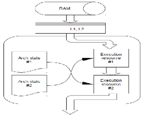
B. Hyperthreading
HT [1] works by duplicating certain sections of the processor those that store the architectural state _ but not duplicating the main execution resources. Hyperthreading is a technology that was introduced by Intel, with the primary purpose of improving support for multi-threaded code. Under certain workloads hyperthreading technology provides a more efficient use of CPU resources by executing threads in parallel on a single processor.
A hyperthreading equipped processor pretends to be two "logical" processors to the host operating system, allowing the operating system to schedule two threads or processes simultaneously. The advantages of hyperthreading are improve support for multi-threaded code, allows multiple threads to run simultaneously, and provides an improved reaction and response time
Figure 2. Hyperthreading
III. SOFTWARE TOOL
The Xilinx Platform Studio (XPS) is used to design Micro Blaze processors. XPS is a graphical IDE for developing and debugging hardware and software. XPS simplifies the procedure to the users, allowing them to
select, interconnect, and configure components of the final system. Dealing with this activity, the student learns to add processors and peripherals, to connect them through buses, to determine the processor memory extension and allocation, to define and connect internal and external ports, and to customize the configuration parameters of the components. Once the hardware platform is built, the students learn many concepts about the software layer, such as: assigning drivers to Peripherals, including libraries, selecting the operative system (OS), defining processor and drivers parameters, assigning interruption drivers, establishing OS and libraries parameters.
An embedded system performed with XPS can be Summarized as a conjunction of a Hardware Platform (HWP) and a Software Platform (SWP), each defined separately.
A. Hardware Platform
The HWP is described in the Microprocessor Hardware Specification (MHS) file; it contains the description of the system architecture, the memory map and the configuration parameters. HWP can be defined as one or more processors connected to one or more peripherals through one or more buses. The definition of the activity follows this sequence:
• To add processors and peripherals. • To connect them through buses.
• To determine the processor memory allocation. • To define and connect internal and external ports. • To customize the configuration parameters of the Components.
B. The Software Platform
The SWP is described in the Microprocessor Software Specification (MSS) file; it contains the description of drivers, component libraries, configuration parameters, standard input/output devices, interruption routines and other software features. The sequence of activities needed to define the SWP
is the following: .
4 All Rights Reserved © 2012 IJARCSEE
• To assign interruption drivers.
• To establish OS and libraries’ parameters.
IV. HARDWARE TOOL
A. Memory and Communication
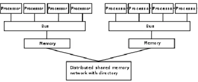
Main memory in a parallel computer is either shared memory (shared between all processing elements in a single address space), or distributed memory (in which each processing element has its own local address space). Distributed memory refers to the fact that the memory is logically distributed, but often implies that it is physically distributed as well. Distributed shared memory and memory virtualization combine the two approaches, where the processing element has its own local memory and access to the memory on non-local processors. Accesses to local memory are typically faster than accesses to non-local memory.
Figure 4 Memory system and communication architecture.
A logical view of a Non-Uniform Memory Access (NUMA) architecture. Processors in one directory can access that directory's memory with less latency than they can access memory in the other directory's memory.
Computer architectures in which each element of main memory can be accessed with equal latency and bandwidth are known as Uniform Memory Access (UMA) systems. Typically, that can be achieved only by a shared memory system, in which the memory is not physically distributed. A system that does not have this property is known as a Non-Uniform Memory Access (NUMA) architecture. Distributed memory systems have non-uniform memory access.
Computer systems make use of caches—small, fast memories located close to the processor which store temporary copies of memory values (nearby in both the physical and logical sense). Parallel computer systems have difficulties with caches that may store the same value in more than one location, with the possibility of incorrect program execution. These computers require a cache coherency system, which keeps track of cached values and strategically purges them, thus ensuring correct program execution. Bus snooping is one of the most common methods for keeping track of which
values are being accessed (and thus should be purged). Designing large, high-performance cache coherence systems is a very difficult problem in computer architecture. As a result, shared-memory computer architectures do not scale as well as distributed memory systems do.
Parallel multiprocessors based on interconnect networks need to have some kind of routing to enable the passing of messages between nodes that are not directly connected. The medium used for communication between the processors is likely to be hierarchical in large multiprocessor machines.
V. APIC
Stands for Advanced Programmable Interrupt Controller Programmable interrupt controller (PIC) is a device that is used to combine several sources of interrupt onto one or more CPU lines, while allowing priority levels to be assigned to its interrupt outputs.
Figure 5. Advanced Programmable Interrupt Controller
VI. THE MICROBLAZE PROCESSOR
Micro Blaze is a 32-bit specific purpose processor Developed by Xilinx in VHDL. It can be parameterized using XPS to obtain an à-la-carte processor. It is a RISC processor, structured as Harvard architecture with separated data and instruction interfaces. Micro Blaze components are divided into two main groups depending on their configurability as shown in Fig.1. Some fixed feature components are:
• 32 general purpose registers sized 32-bit each. • Instructions with 32 bits word-sized, with 3 operands and 2 addressing modes.
• 32 bits address bus. • 3-stage Pipeline.
Some of the most important configurable options are: • An interface with OPB (On-chip Peripheral Bus) data bus.
• An interface with OPB instruction bus.
• An interface with LMB (Local Memory Bus) data bus.
5 All Rights Reserved © 2012 IJARCSEE
• To include EDK libraries.
• To select the operative system (OS). • To define processor and drivers’ parameters. • Data cache.
• 8 Fast Simplex Link (FSL bus) Interfaces. • Cache Link bus support.
• Hardware exception support. • Floating Point Unit (FPU).
The suggested core embedded processor contains a dual-issue, superscalar, pipelined processing unit, Along with the other functional elements required to Implement embedded SoC solutions. This other Functions include memory management and timers.
VI. PRACTICAL DESIGNS
Practical sessions introduce gradual learning, allowing the fast design based on previous sessions. Essential problems in hardware programming will be raised: • HyperTerminal serial communication.
• Using IO ports. • Memory controller.
• Interruption routines and priority.
• Message passing in multiprocessors communication. Relation between practices is shown. For instance, 5th session is based on all previous sessions, 7th session is based on 3rd and 1st Session.
Figure 6. Hardware of Embedded Multiprocessor Processor
SRAM external memory is added to the system at fourth session. Next session is dedicated to the External Memory Controller and how to split the bus. Micro Blaze interruptions are added in the sixth session, and external interruptions using the interruption controller are included in the seventh session. Finally, students build a biprocessor, using the Fast Simple Link channel at session eight. In fig. 6.
Relation between practices is shown. For instance, 5th session is based on all previous sessions, 7th session is based on 3rd and 1st Session.
VII. MULTICORE SYSTEM AND THEIR CATCHES
Figure 7. Multicore system and their catches
Type of cache sharing depends on the system: it can be L2 that is shared.The memory consistency model for a shared-memory multiprocessor specifies the behaviour of memory with respect to read and write operations from multiple processors. We focuses on providing a balanced solution that directly addresses the trade-off between programming ease and performance.
A. Types of Coherence Protocols
Directory-based: The data being shared is placed in a common directory that maintains the coherence between caches. The directory acts as a _lter through which the processor must ask permission to load an entry from the primary memory to its cache. When an entry is changed the directory either updates or invalidates the other caches with that entry.
Snooping: individual caches monitor address lines for accesses to memory locations that they have cached. When a write operation is observed to a location that a cache has a copy of, the cache controller invalidates its own copy of the snooped memory location.
Figure 8. Caches coherency protocol example: MESI
B. SMP
Stands for Symmetric Multi Processing
Identical processing units
Single shared memory
Single bus, mesh interconnections
C. NUMA
6 All Rights Reserved © 2012 IJARCSEE
Stands for Non Uniform Memory Access Memory access time depends on the memory location relative to a processor. Under NUMA, a processor can access its own local memory faster than non-local memory.
Highly scalable
Requires special coherency protocols
Requires OS support
D. Boot process
1. The BSP1 executes the BIOS's boot-strap code to configure the APIC environment, sets up system-wide data structures, starts and initializes the AP2s. When the BSP and APs are initialized, the BSP then begins executing the operating-system initialization code. 2. Following a power-up or reset, the APs complete a minimal self-configuration, then wait for a startup signal (a SIPI message) from the BSP processor. Upon receiving a SIPI message, an AP executes the BIOS AP configuration code, which ends with the AP being placed in halt state.
1Boot strap processor. 2Application processor
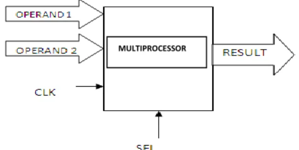
VIII. BIPROCESSOR SYSTEM DESIGN
The last and most complex practical session is the design and implementation of a biprocessor. A computational system composed of two Micro Blazes will be designed. Both Micro Blazes will be interconnected using message-passing protocol. Each Micro Blaze has its own non-shared memory for Instructions and data. In the Fig. 3 a diagram with the structure of the design is shown. In it, the buses and components used have been detailed. It also includes how they are interconnected At first, following the logical sequence exposed previously, a HWP will be created. This HWP will include the configuration of the components and buses, their interconnection, the memory map, ports and other parameters. In the following subsection, the steps needed to configure the system will be described. The parameters shown in this section depends on the FPGA chip, in this case the Spartan 3 board [11].
A. Hardware Platform Specifications
This stage is described in the MHS file. Following, the Components specified in the structure of the system are enumerated:
• Two Micro Blaze processors.
• Two on-chip RAM memory blocks (BRAM), one for Each processor.
• One UART.
• One OPB bus, to connect the UART with the slave
Processor.
• Two LMB buses to communicate each processor with Their respective data memory controller; and another Two LMB buses to interconnect the processors with Their instruction memory controller.
• One FSL channel to intercommunicate each processor with the other.
A valid set of parameters for the UART and Micro Blaze are the following:
1) UART parameters.
a) C_CLK_FREQ = 50_000_000. Set the frequency of the OPB bus, connected to the UART. It has to coincide with the operational system speed.
b) C_BAUDRATE = 19200. Set the bauds for the UART. The terminal used to receive characters has to be configured at the same baud rate.
c) C\_USE\_PARITY = 0. Set whether the UART should work with parity bit or not.
SOFTWARE AND HARDWARE REQUIREMENT
For Software simulation I will prefer MODELSIM and for synthesis I will be prefer XILINX. Hardware requirement is SPARTAN-3.
TEST BENCH FOR MULTIPROCESSOR
LIBRARY IEEE;
USE IEEE.STD_LOGIC_1164.ALL; USE IEEE.STD_LOGIC_ARITH.ALL;
ENTITY E_TestBench IS END E_TestBench;
ARCHITECTURE A_TestBench OF E_TestBench IS
COMPONENT E_MultiProcessor PORT
(
clk:IN STD_LOGIC;
jmp_address:IN STD_LOGIC_VECTOR(11 DOWNTO 0);
jmp_en:IN STD_LOGIC
result:OUT STD_LOGIC_VECTOR(7 DOWNTO 0);
current_address:OUT
STD_LOGIC_VECTOR(11 DOWNTO 0) );
END COMPONENT;
SIGNAL s_clk:STD_LOGIC := '0'; SIGNAL
s_jmp_address:STD_LOGIC_VECTOR(11 DOWNTO 0);
7 All Rights Reserved © 2012 IJARCSEE
SIGNAL s_result:STD_LOGIC_VECTOR(7 DOWNTO 0);
SIGNAL
s_current_address:STD_LOGIC_VECTOR(11 DOWNTO 0);
BEGIN
MP:E_MultiProcessor PORT
MAP(s_clk,s_jmp_address,s_jmp_en,s_result,s_current _address);
s_clk <= NOT(s_clk) AFTER 100 ns; s_jmp_address <= (OTHERS => '0'); s_jmp_en <= '0';
END A_TestBench;
Figure 9.Hardware of Embedded Multiprocessor
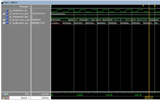
Figure 10.Simulation Result of Multiprocessor
ACKNOWLEDGEMENTS
Authors wish to remark the great task carried out by the Xilinx and Modelsim user guide; and the authors wish to thank Prof.C.N.Bhoyar for his contribution in the design process.
REFERENCES
[1] John L. Hennessy and David A. Patterson. Computer architecture: a quantitative approach. Morgan Kaufmann Publishers Inc., San Francisco, CA, USA, fourth edition 2007. [2] Doug Burger and James R. Goodman. Billion-Transistor Architectures: There and Back Again. IEEE Computer, 37(3):22–28, 2004.
[3] David Geer. Industry Trends: Chip Makers Turn to Multicore Processors. Computer, 38(5):11–13, May,2005.
[4] AMD Corporation. Multi-core processors: the next revolution in computing White paper, 2005.
[5] B. Ackland, A. Anesko, D. Brinthaupt, S.J. Daubert, A. Kalavade,J. Knobloch, E. Micca, M. Moturi, C.J. Nicol, J.H. O’Neill, J. Othmer, E. Sackinger, K.J. Singh, J. Sweet, C.J. Terman, and J. Williams. A Single-chip, 1.6-billion, 16-b MAC/s Multiprocessor IEEE Journal of, 35(3):412–424, Mar2000.
[6] Asawaree Kalavade, Joe Othmer, Bryan Ackland, and K. J. Singh.Software environment for a multiprocessor DSP. In DAC 99: Proceedings of the 36th ACM/IEEE conference on Desig automation, pages 827–830, New York, NY, USA, 199 ACM.
[7] V. Sklyarov, and I. Skliarova. ―Teaching Reconfigurable Systems: Methods, Tools, Tutorials, and Projects,‖ IEEE Trans. on Education,vol. 48, no. 2, 290–300, 2005. [8] OpenSPARC http://www.opensparc.net/edu/university- program.html. Last accessed on 8th November 2009.
[9] ―Platform Studio User Guide,‖ Application notes, Xilinx, 2005.
[10] ―Microblaze Processor Reference Guide,‖ Application notes, Xilinx.2005.
[11] ―Embedded System Tools Reference Manual,‖ Application notes,Xilinx, 2008.
[12] ―OS and Libraries Document Collection,‖ Xilinx, Application notes September 2007.
Sumedh S,Jadhav M.Tech in VLSI Department of Electronics Engineering, International Journal paper titled ―HDL- BASED EMBEDDED MULTIPROCESSOR ARCHITECTURE USING FPGA‖ published in International Journal of Engineering Research and Applications (IJERA), International Journal paper titled ―IMPLEMENTATION OF FINGERPRINT ASSIST WENDING MACHINE WITH RECHARGE OPTION‖ published in International Journal of Electrical and Electronics Engineering (IJEEE) ISSN (PRINT): 2231 – 5284 , VOL-I , International Journal paper titled ―FPGA BASED EMBEDDED MULTIPROCESSOR ARCHITECTURE‖ published in International Journal of Electrical and Electronics Engineering (IJEEE) ISSN (PRINT): 2231 – 5284 , VOL-I , International Journal paper titled ―DESIGN AND IMPLEMENTATION OF EMBEDDED MULTIPROCESSOR ARCHITECTURE USING VHDL‖ published in International Journal of Electronics Signals and Systems (IJESS) ISSN:2231- 5969 , VOL-I , International Journal paper titled ―HDL - BASED EMBEDDED MULTIPROCESSOR ARCHITECTURE‖ published in International Journal of Engineering and technology UK April 2012, International Journal paper titled ―EMBEDDED
MULTIPROCESSOR ARCHITECTURE USING VHDL” published
in International Journal of Computer & Communication Technology (IJCCT) ISSN (ONLINE):2231-0371 ISSN(PRINT):0975-7449,
International Journal Paper Titled ―EMBEDDED
8 All Rights Reserved © 2012 IJARCSEE
increases and the exploitation of instruction- level parallelism. We will be designing embedded multiprocessor based on Xilinx environment.
Prof.C.N.Bhoyar M.E in VLSI Priyadarshini college of Engineering Department of Electronics Engineering, Nagpur State- Maharashtra, India. International Journal paper titled ―HDL- BASED EMBEDDED MULTIPROCESSOR ARCHITECTURE USING FPGA‖ published in International Journal of Engineering Research and Applications (IJERA, International Journal paper titled ―FPGA BASED EMBEDDED MULTIPROCESSOR ARCHITECTURE‖ published in International Journal of Electrical and Electronics Engineering (IJEEE) ISSN (PRINT): 2231 – 5284 , VOL-I ,
International Journal paper titled ―DESIGN AND
IMPLEMENTATION OF EMBEDDED MULTIPROCESSOR ARCHITECTURE USING VHDL‖ published in International Journal of Electronics Signals and Systems (IJESS) ISSN:2231- 5969 , VOL-I , International Journal paper titled ―HDL - BASED EMBEDDED MULTIPROCESSOR ARCHITECTURE‖ published in International Journal of Engineering and technology UK April 2012, International Journal paper titled ―EMBEDDED
MULTIPROCESSOR ARCHITECTURE USING VHDL” published
in International Journal of Computer & Communication Technology (IJCCT) ISSN (ONLINE):2231-0371 ISSN(PRINT):0975-7449,
International Journal Paper Titled ―EMBEDDED