52 All Rights Reserved © 2012 IJARCSEE
VLSI Design and Optimized Implementation of a MIPS RISC
Processor using XILINX Tool
Neeraj Jain
Research Scholar (M.Tech. VLSI), Mewar University, Chittorgarh
Summary
In this paper I have described the design of a 16-bit Optimized MIPS RISC processor for applications in real-time embedded systems and also I tried to compare that with the RISC processor having an ease of pipelining. RISC is a design philosophy that has become a mainstream in scientific and engineering applications[7]. The processor executes most of the instructions in single machine cycle making it ideal for use in high speed systems. The processor is designed and implemented on an FPGAboard Spartan XC2S20C (Spartan 2E) using VHDL and VERILOG[5]such that one can reconfigure it according to specific requirements of the target applications. The processor is powerful enough to be used as a stand-alone processing element and is generic enough to be used in multi-processor System on Chip.
Keywords:
RISC processor, Pipelining, VLSI, FPGA, and Computer Architecture, Real-time embedded systems, System on Chip (SoC)
1. Introduction
In today’s era of area optimization, high speed systems and ubiquitous computing, the need for real-time embedded systems is always on the rise. These embedded systems must operate within stringent requirements that are often at the intersection of the
conflict between speed and area. Increasing complexity of signal processing in embedded real-time applications requires very high computational power and also optimizes area. This power can be achieved by high performance programmable components like RISC or CISC processors. Naturally, to enhance the speed of such systems we need to design algorithms that can compete with low running time complexity. Another way of optimize circuit to reduce delay and also increasing the speed of the system is to directly design high speed VLSI chips for these embedded systems. The present paper focuses on to optimize area to reduce delay and also change the sequencing of components using Routing Methods, Optimization consists of different levels, according to how fast the optimizations can be performed and the nature and extent of the work.
53 All Rights Reserved © 2012 IJARCSEE
The paper has been organized as follows: in the next section 2 we will review the design of the processor and discuss concept of RISC using two optimizing concepts viz. compilation techniques and global optimization. In the section 3Micro-Architecture and module design of 16-bit RISC Processor[6] and different RTLs are viewed. Section 4 & 5 is dedicated to the discussion of its simulation results & advantages and disadvantages followed by section 6 where conclusion of paper with future directions of the work is presented.
2. Concept of RISC
Overall design procedure is composed of pipeline, stage analysis, instruction execution analysis, RT-level (Register Transfer Level) functional unit composition, and control signal generation.
The design of processor is based on certain assumptions. One is that the design must have few registers. Another assumption is that RISC based processor is more suitable for real-time embedded systems than a CISC processor. RISC architecture reduces the complexity of the design and also it becomes possible to speed-up the execution time. With CISC processor it is possible to speed up the operation time but it will prove to be difficult.
The million instruction per secondsreduced instruction set computer (MIPS RISC), CPU design philosophy that favors a smaller and simpler set of instructions that all take about the same amount of time to execute. The most common MIPS RISC microprocessors are SPARC, MIPS, ARM, DEC Alpha, PA-RISC, and IBM's PowerPC etc... The idea was inspired by the discovery that many of the features that were included in traditional Control processing unit designs to facilitate coding were being ignored by the programs that was running on them. Also these more
complex logic features took several microprocessor cycles to be performed. Additionally, the performance gap between the processor and main memory was increasing. This led to a number of techniques to streamline processing within the CPU, while at the same time attempting to reduce the total number of memory accesses.
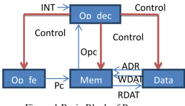
With above assumptions, the basic block diagram of the processor.
Figure 1 Basic Block of Processor
There are two techniques to optimize circuits
(I) Compilation Techniques
Key to machine-specific optimization is instruction scheduling. The MIPS processor is designed to make all processor units visible to software, which allows the compiler to emit instructions in an order that utilizes each unit to its maximum efficiency. Rather than providing expensive scheduling and interlocking in hardware, the compiler is relied upon to ensure consistency between instructions. This optimization improves performance by an average of 20%.
(II) Global Optimization
The MIPS global optimizer[3] performs all the common global optimizations. While these optimizations are not machine-specific, they are more effective on RISC
Op_dec oder
Data core Mem
Op_fe tch
Control
Control INT
Pc
Opc
Control
54 All Rights Reserved © 2012 IJARCSEE
machines than on conventional ones. First, the low level of the machine functions exposes more candidates for global optimization. Second, the effects to these global optimizations are likely to be beneficial, since they are not replaceable by more complex machine instructions in RISC architecture. MIPS has refined the U-Code intermediate language to make it exposé most MIPS machine primitives to the optimizer. Also, most of the optimizations were specifically tuned to the MIPS environment.The global optimizer also provides global register allocation. The load/store nature of RISC machines makes register allocation especially effective. By globally analyzing usage patterns, the register allocator decides which variables best reside in registers.
3. Micro-Architecture and module
design of 16-bit RISC Processor
The micro-architecture[1]refers to a view of the machine that exposes the registers, buses and all other important functional units such as ALUs and counters. The principle subsystems of a processor are the CPU, main memory and the input/output. The data path and the control unit interact to do the actual processing task. The control unit receives signals from the data path and sends control signals to the data path. These signals control the data flow within the CPU and between the CPU and the main memory and Input/ Output.
The processor has 16-bit instruction words and 16 general purpose registers. Every instruction is completed in four cycles. An external clock is used as the timing mechanism for the control and data path units. This section includes a summary of the main features of the processor, a description of the pins, and a high level diagram of the external interface of the chip.
(I) 16 instructions in the instruction set architecture.
(II) External Clock is used.
(III) Instruction completion in 4 clock cycles (IV)16 general purpose registers.
(V) 14 external address lines.
A. ALU
Figure 2 Top Block of ALU
55 All Rights Reserved © 2012 IJARCSEE
B. MEMORY
Figure 4 RTL view of Memory unit
C. RAM
Figure 5 RTL view of RAM
D. RISC TOP
Figure 6 Block diagram of RISC-16 bit processor
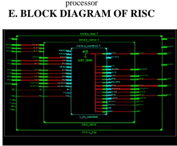
E. BLOCK DIAGRAM OF RISC
Figure 7 Pin diagram of RISC-16 bit processor
4. Simulation Results
56 All Rights Reserved © 2012 IJARCSEE
Figure 9 Data Path Simulation Result
5. Advantages and Disadvantages
There are several advantages of this design; the first is the generic design of the processor at the HDL level such that it is possible to re-configure the processor for specific application. Another is the use of less internal registers and more FPGA memories for reducing the design complexity of the processor.
However, despite having several advantages, there are few disadvantages of the design like we always has to define I/O module for each design so we require a generic one. Another is that HDL code is specific for a target FPGA so can’t be useable for other FPGA platform.
6. Conclusion& Future Work
In this paper I presented the design of 16-bit RISC processor in VHDL and also on VERILOG. The FPGA implementation of the MIPS RISC Microprocessor[9] and tools involved here represent my goal of introducing FPGAs implementation to design computer architecture. The development board and tools introduced could easily be integrated into the computer architecture.
Future work is to implement a design with generic I/O module which is applicable for any standard FPGA. Also a processor with clock gating technique can be implemented which mainly reduces the dynamic power consumption.
References
[1]. Xia Li, LongweiJi, Bo Shen, Wenhong Li and Qianling Zhang, "VLSI Implementation of a High-performance
32-bit RISC Microprocessor," International Conference on Communications,
Circuits and Systems and West Sino Expositions, IEEE 2002, Vol. 2, pp.1458-1461.
[2]. Sivarama P. Dandamudi, "Fundamentals of Computer Organization and design" Springer-Verlag New York, Inc., 2003. [3]. SamiappaSakthikumaran et al., “A Novel Low Power and High Speed Wallace Tree Multiplier for RISC Processor”, 3rd International Conference on Electronics Computer Technology - ICECT 2011. [4]. A 32-b RISC Implemented in Enhancement-Mode JFET Ga As Rasset, T.L.;Niederland,R.A.;Lane,J.H,Geideman, W.A.;McDonnellDouglas Astronautics Company, Huntington Beach, CA 92647 Date of Current Version: 27 March 2009 [5]. VHDL-based development of a 32-b pipelined RISC processor for educational Purposes Buhler, M. Baitinger, U.G. Stuttgart Univ. Date of Current Version: 06 August 2002
[6] MIPS Technologies, www.mips.com. [7] MIPS RISC PROCESSOR WHITE PAPER
[8] Altera, MAX+PLUS II Getting Started Manual, ver. 6.0, 2005.
[9] Diab, H., Demashkieh, I., “A reconfigurable microprocessor teaching tool”, IEEE Proceedings A, vol. 137, issue 5, September 2009.