WD5125C
2.5A Buck-Boost Converters with I
2C
Interface
Descriptions
The WD5125C is a high efficiency, high output current buck-boost converter fully programmable through I2C. Depending on the input voltage, it can automatically operate in boost, buck or in a novel 4-cycle buck-boost mode when the input voltage is approximately equal to the output voltage. The transitions between modes happen at defined thresholds and avoid unwanted toggling within the modes to reduce output voltage ripple. Two registers, accessible through I2C, set the output voltage, and a VSEL pin selects which output voltage register is active. Thus the devices can support dynamic voltage scaling. If the output voltage register is changed during operation or the VSEL pin is toggled, the device transits in a defined, programmable ramp-rate.
The WD5125C is available in a 2.2mm×1.3mm CSP-15L package. Standard products is Pb-Free and Halogen-Free.
Features
⚫ Input Voltage Range : 2.2V to 5.5V
⚫ Output voltage range: 1.8 V to 5.2 V
◆ I2C-configurable during operation and shutdown
◆ VSEL pin to toggle between two output voltage presets
⚫ Peak current mode buck-boost architecture
◆ Defined transitions between buck, buck-boost and boost operation
◆ Forward and reverse current operation
◆ Start-up into pre-biased outputs
⚫ Safety and robust operation features ◆ Integrated soft start
◆ Overtemperature and overvoltage protection
◆ True load disconnect during shutdown
◆ Forward and backward current limit
⚫ Pre-programmed output voltages (3.3 V, 3.45 V)
⚫ High efficiency over entire load range ◆ Low 13 μA operating quiescent current
◆ Automatic power save mode and forced PWM mode (I2
C-configurable)
Http//:www.ovt.com
CSP-15L EN C B A AGND VSEL VIN LX1 GND SCL LX2 D VIN LX1 GND LX2
SDA VOUT VOUT
E
1 2 3
Pin configuration (Top view)
= Device code = Special code
Y = Year code
W = Week code
Marking
Applications
⚫ System pre-regulator ⚫ Point-of-load regulation ⚫ Thermoelectric device supply
⚫ Broadband network radio or SoC supply
Order information
Device Package Shipping
Typical Applications
VIN VOUT
LX1
L1
V
INWD5125
C
OUT2 X 22uF
C
IN 10uFV
OUTVSEL GND
ON/OFF
ENSCL SDA
AGND
LX2
H/L
0.47uH
Pin Descriptions
Pin NO. Symbol I/O Descriptions
A1 EN I Device enable. A high logic level on this pin enables the device; a low logic level on this pin disables the device.
A2 VIN — Supply voltage for power stage A3 VIN — Supply voltage for power stage
B1 VSEL I
This pin selects which VOUT register is active. When a low logic level is applied to this pin, the VOUT1 register sets the output voltage. When a high logic level is applied to this pin, the VOUT2 register sets the output voltage.
B2 LX1 — Inductor connection B3 LX1 — Inductor connection C1 AGND — Analog ground
C2 GND — Power ground
C3 GND — Power ground
D1 SCL I/O I2C serial interface clock. Pull this pin up to the I2C bus voltage with a resistor or a current source.
D2 LX2 — Inductor connection D3 LX2 — Inductor connection
E1 SDA I/O I2C serial interface data. Pull this pin up to the I2C bus voltage with a
resistor or a current source.
E2 VOUT — Converter output
Block Diagram
ControlLogic
and PWM Logic VIN OVP
Gate Drive Gate Drive
I2C Interface
Compensation Net Isense
Isense Vref
PGND
VOUT
VIN
EN
VSEL
SDA
SCL
VOUT Discharge
EA
Comparator
AGND
LX1
LX2
Absolute Maximum Ratings
Recommended Operation Conditions
(2)Parameter Symbol Value Unit
Input voltage VIN, LX1, LX2, VOUT, SCL, SDA, EN, VSEL -0.3~+6 V
Input voltage for less than 10 ns LX1, LX2 -3~9 V
Thermal Characteristics (1) RθJA 80.5
oC/W
RθJC 0.6 oC/W
Maximum Junction Temperature TJ 150 oC
Operating Ambient Temperature Topr -40 ~ 85 oC
Storage Temperature Tstg -65 ~ 150 oC
ESD Classification HBM ±2000 V
Symbol Characteristics Min. Typ. Max. Unit
VIN Supply Voltage 2.2 5.5 V
VOUT Output Voltage
Low range 1.8 4.975
V
High range 2.025 5.2
VIH High-level input voltage SCL, SDA, VSEL 1.3 VI
V
VIL Low-level input voltage SCL, SDA, VSEL 0 0.3
VEN Input voltage EN 0 VI V
IO Output current
VO = 3.3 V, VI ≥ 2.5 V 2.5
A
VO = 3.5 V, VI ≥ 2.5 V 2
VO = 3.5 V, VI ≥ 2.8 V 2.5
VO = 3.3 V, VI ≥ 3 V 3
CIN Input capacitance, effective value 5 µF
CO Output capacitance, effective value 13 16 µF
L Inductance, effective value 0.39 0.47 0.56 µH
TA Operating free-air temperature -40 - 85 ℃
TJ Operating junction temperature -40 - 125 ℃
These are stress ratings only. Stresses exceeding the range specified under “Absolute Maximum Ratings” may cause substantial damage to the device. Functional operation of this device at other conditions beyond those listed in the specification is not implied and prolonged exposure to extreme conditions may affect device reliability.
Note 1: Surface mounted on FR-4 Board using 1 square inch pad size, dual side, 1oz copper. Note 2: The device is not guaranteed to function outside of its operating conditions.
Electronics Characteristics
VIN = 3.6 V, VOUT = 3.3 V, Typical values are at TJ = 25°C, unless otherwise noted.
PARAMETER TEST CONDITIONS MIN TYP MAX UNIT
SUPPLY AND THERMAL PROTECTION IQ;VIN Supply current into VIN
VI = 3.6 V, VO = 3.3 V, V(EN) = 3.6 V, not switching 14 µA
VI = 3.6 V, VO = 0 V, V(EN) = 3.6 V, Output disabled
with ENABLE bit in Control Register 13 µA ISD Shutdown current into VIN VI = 3.6 V, VO = 0 V, V(EN) = 0 V 0.5 µA
VIT+ Under-voltage lockout threshold VUVLO rising 2 2.1 2.2 V
VIT-HYS UVLO threshold voltage hysteresis VUVLO-HYS 150 mV
TOTP Thermal shutdown temperature Junction temperature rising 155 °C
TOTP-HYS Thermal shutdown hysteresis 20 °C
I/O SIGNALS
VIT+
Positive-going input threshold voltage
SCL, SDA, VSEL 1.17
V
EN 1.07 1.1 1.13
V
IT-Negative-going input threshold voltage
SCL, SDA, VSEL 0.42
V
EN 0.97 1 1.03
VHYS Hysteresis voltage EN 40 mV
IIH High-level input current SCL, SDA, VSEL V(SCL) = V(SDA) = V(VSEL) = 1.8 V, no pullup resistor ±0.01 ±0.1
µA
IIL Low-level input current SCL, SDA, VSEL V(SCL) = V(SDA) = V(VSEL) = 0 V, no pullup resistor ±0.01 ±0.1
IOL Low-level output current SCL, SDA VOL = 0.4 V 20 mA
IIB Input bias current EN V(EN) = 0 V to 5.5 V ±0.01 ±0.1 µA
POWER STAGE
VO
Output voltage range Low range 1.8 4.975 V
High range 2.025 5.2
Output voltage accuracy PWM operation –1.5 1.5 %
PSM operation –1.5 3.5
Default output voltage (RANGE = 0) VSEL = low 3.3 V
VSEL = high 3.45
ILIMIT Switch current limit
VI = 2.9 V, VO = 3.6 V,
boost operation, output sourcing current 5.2 6.5
A VI = 4.1 V, VO = 3.3 V,
buck operation, output sourcing current 3.8 4.3 5.2 VI = 5 V, VO = 3.3 V,
reverse-boost operation, output sinking current –1.3 –0.35 IT–(PSM) PSM entry threshold (peak) current VI = 4.2 V; VO = 3.3 V 0.85 A
IDISCHARGE Output discharge current VI = 3.6 V, VO ≥ 0.8 V 50 mA
VT+(PG) Positive-going power-good threshold voltage 95
%
VT–(PG) Negative-going power-good threshold voltage 90
VINOV Positive-going input overvoltage threshold 5.7 V
I2C INTERFACE
Timing Requirements
Over operating junction temperature range and recommended supply voltage range (unless otherwise noted)
PARAMETER TEST CONDITIONS MIN TYP MAX UNIT
fSCL SCL clock frequency
Standard mode 0 100
kHz
Fast mode 0 400
Fast mode plus 0 1000
tLOW LOW period of the SCL clock
Standard mode 4.7
µS
Fast mode 1.3
Fast mode plus 0.5
tHIGH HIGH period of the SCL clock
Standard mode 4.0
µS
Fast mode 0.6
Fast mode plus 0.26
tBUF
Bus free time between a STOP and a START condition
Standard mode 4.7
µS
Fast mode 1.3
Fast mode plus 0.5
tSU;STA
Set-up time for a repeated START condition
Standard mode 4.0
µS
Fast mode 0.6
Fast mode plus 0.26
tHD;STA
Hold time (repeated) START condition
Standard mode 4.0
µS
Fast mode 0.6
Fast mode plus 0.26
tSU;DAT Data set-up time
Standard mode 250
nS
Fast mode 100
Fast mode plus 50
tHD;DAT Data hold time
Standard mode 0
µS
Fast mode 0
Fast mode plus 0
tr
Rise time of both SDA and SCL signals
Standard mode 1000
nS
Fast mode 20 300
Fast mode plus 120
tf
Fall time of both SDA and SCL signals
Standard mode 300
nS Fast mode 20×VDD/5.5 300
Fast mode plus 20×VDD/5.5 120
tSU;STO Set-up time for STOP condition
Standard mode 4.0
µS
Fast mode 0.6
Fast mode plus 0.26
tVD;DAT Data valid time
Standard mode 3.45
µS
Fast mode 0.9
Timing Requirements (continued)
Over operating junction temperature range and recommended supply voltage range (unless otherwise noted)
PARAMETER TEST CONDITIONS MIN TYP MAX UNIT
tVD;ACK Data valid acknowledge time
Standard mode 3.45
µS
Fast mode 0.9
Fast mode plus 0.45
Cb Capacitive load for each bus line
Standard mode 400
pF
Fast mode 400
Fast mode plus 550
tW(VSEL) VSEL pulse duration VSEL = high or low 5 µS
Switching Characteristics
VIN = 3.6 V, VOUT = 3.3 V, Typical values are at TJ = 25°C, unless otherwise noted.
PARAMETER TEST CONDITIONS MIN TYP MAX UNIT
td(EN)
Delay between a rising edge on the EN pin
and the start of the output voltage ramp TJ = 25°C, VI = 3.6 V 270 450 µS td(PG) Power-good delay VO falling 50 µS
SR Slew rate of internal ramp during dynamic voltage scaling
SLEW = 00b, forced-PWM operation ±1
V/mS SLEW = 01b, forced-PWM operation ±2.5
SLEW = 10b, forced-PWM operation ±5 SLEW = 11b, forced-PWM operation ±10
fSW Inductor Switching Frequency no Load, PWM operation 1.9 2.25 2.6 MHz
td(VSEL)
Delay between rising edge of VSEL and
Typical Characteristics
Operation Informations
The WD5125C is a high-efficiency buck-boost converters that integrated four switches internally to achieve high efficiency power conversion over a wide range of input voltages and output currents. It can automatically switches between buck, boost, and buck-boost operation depends on the operating conditions.
Feature Description
Operation ModeThe device could automatically select the best operation mode (buck, boost or buck-boost) depends on operation condition as showed below:
Boost Buck - Boost Buck
VI < VO VI = VO VI > VO
Hysteresis Hysteresis
Figure x. Operation Mode Selection
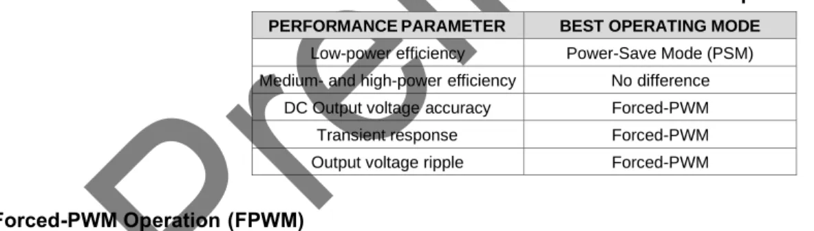
Power-Save Mode Operation (PSM)
To increase efficiency across the wide range of operating conditions, the device automatically changes from PWM at medium and high load conditions to PSM at light load condition.
To enable power-save mode, clear the FPWM bit in the Control register to 0.
Table 1. FPWM versus PSM Performance Comparison
PERFORMANCE PARAMETER BEST OPERATING MODE Low-power efficiency Power-Save Mode (PSM) Medium- and high-power efficiency No difference
DC Output voltage accuracy Forced-PWM Transient response Forced-PWM Output voltage ripple Forced-PWM
Forced-PWM Operation (FPWM)
The device always operates in PWM mode if FPWM mode bit has been set in Control register. FPWM operation has lower output voltage ripple and better transient response than power-save mode operation, but lower efficiency at low output currents (see Table 1).
Note that the device inhibits forced-PWM operation during start-up (that is, until the converter output has reached power-good for the first time).
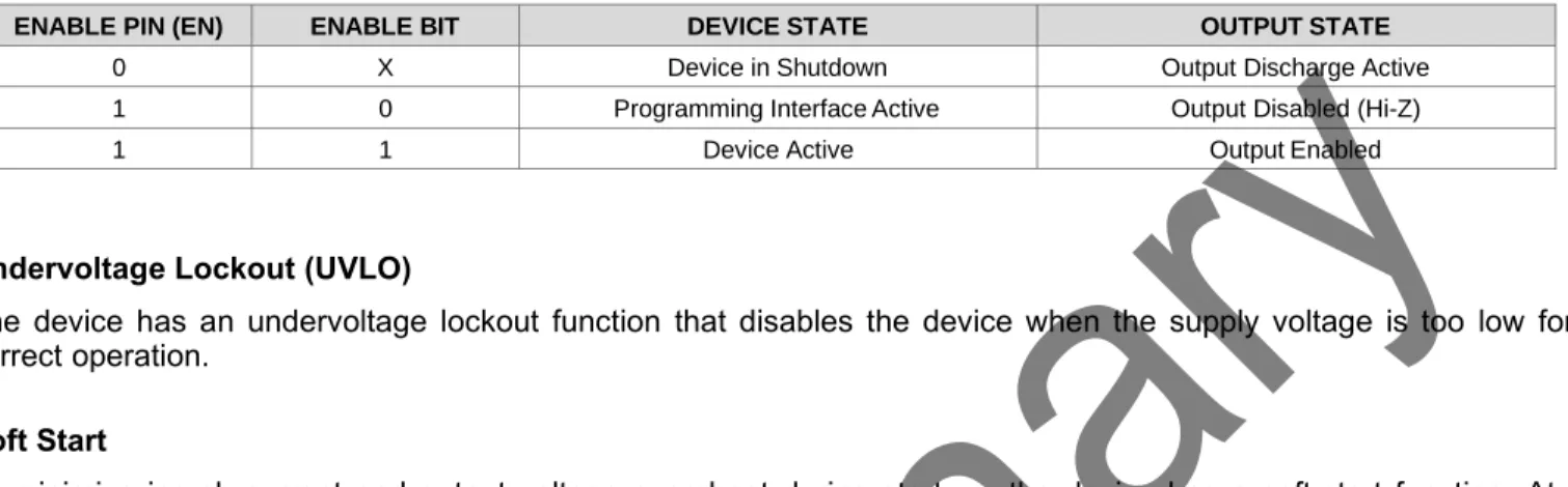
Enable (EN)
The EN pin enables and disables the device, high enable the device and low disable the device.
You can also use the ENABLE bit in the Control register to enable and disable the output of the converter (see the
Register Map).
Table 2. Device Enable Truth Table
ENABLE PIN (EN) ENABLE BIT DEVICE STATE OUTPUT STATE
0 X Device in Shutdown Output Discharge Active
1 0 Programming Interface Active Output Disabled (Hi-Z)
1 1 Device Active Output Enabled
Undervoltage Lockout (UVLO)
The device has an undervoltage lockout function that disables the device when the supply voltage is too low for correct operation.
Soft Start
To minimize inrush current and output voltage overshoot during start-up, the device has a soft-start function. At turn on, the switch current limit ramps gradually to its maximum value and the device starts up in a controlled way. The gradual increase of the current limit generates the smallest inrush current for no-load conditions. It is also possible to start into a high load as long as the load does not exceed the device current limit.
The rise time of the output voltage changes with the application circuit and the operating conditions. The output voltage rise time increases if the following occurs:
• The output capacitance is large. • The load current is large.
• The device operates in boost mode. Output Voltage Control
The device supports output voltage range from 1.8 V to 5.2 V with a resolution of 25 mV. To set the needed output voltage, you must first program the RANGE bit in the Control register to select the output voltage range:
• When RANGE = 0, you can program the output voltage from 1.8 V to 4.975 V. • When RANGE = 1, you can program the output voltage from 2.025 V to 5.2 V.
Then you can program the VOUT1 register and VOUT2 register to set the output voltage: • When RANGE = 0, VO = (VOUT[6:0] × 0.025) + 1.8 V
• When RANGE = 1, VO = (VOUT[6:0] × 0.025) + 2.025 V
VOUT[6:0] is the 7-bit value in the VOUT1 register or VOUT2 register, whichever is active.
The VSEL pin selects which VOUT register is active:
• When VSEL = low, the VOUT1 register sets the output voltage. • When VSEL = high, the VOUT2 register sets the output voltage.
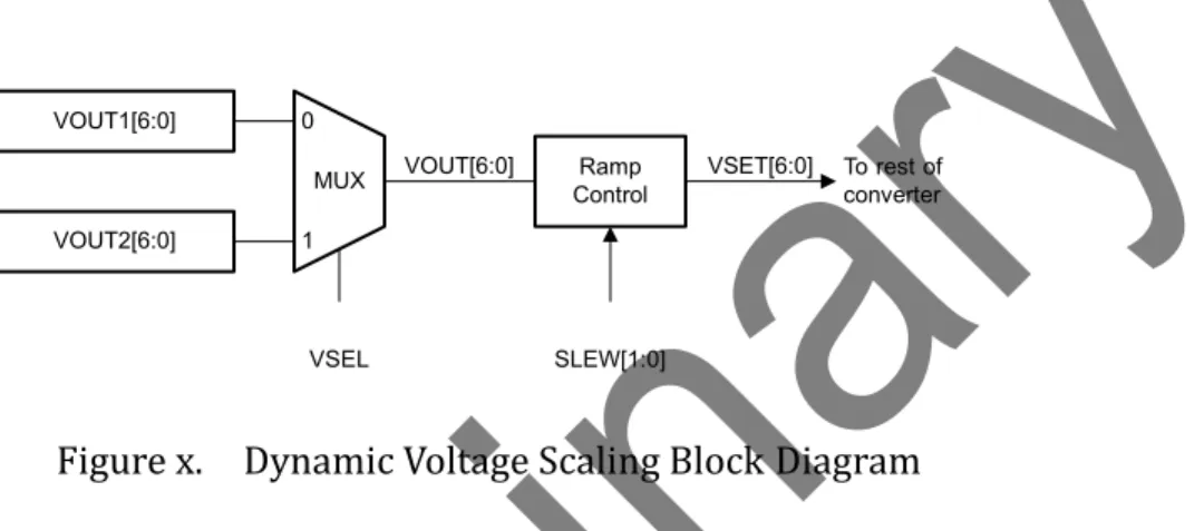
Dynamic Voltage Scaling
The device supports dynamic voltage scaling (DVS) function which lets you change the output voltage in a controlled way during operation.
Figure x shows a simplified block diagram of the DVS function. The VSEL pin selects either the VOUT1 register or the VOUT2 register to control the output voltage. The ramp control block detects when the target output voltage is different from the actual output voltage and ramps the output voltage to the target voltage in 25-mV steps. 2-bit SLEW parameter in the Control register is been used to select one of four slew rates from 0.5 V/ms to 10 V/ms.
The device starts a DVS ramp when you change the logic level on the VSEL pin or program to a new value in the active VOUT register.
VOUT1[6:0]
VOUT2[6:0]
0 MUX 1
VOUT[6:0] Ramp
Control
VSET[6:0] To rest of converter
VSEL SLEW[1:0]
Figure x. Dynamic Voltage Scaling Block Diagram
Note that if you change the contents of the active VOUT register or change the state of the VSEL pin during start-up (that is, before the end of the soft start), the converter uses the new value immediately and does not ramp gradually to the final value.
Figure x shows the timing diagram when you use the VSEL pin to change between the output voltage values in the VOUT1 and VOUT2 registers.
VSEL
VO
tr = tf = Where
IVO(1) - VO(2) I
SR
▪ VO(1) is the output voltage set by the VOUT1 register
▪ VO(2) is the output voltage set by the VOUT2 register
▪ SR is the slew rate set by the SLEW bits in the CONTROL register
Figure x. DVS Timing Diagram Using the VSEL Pin
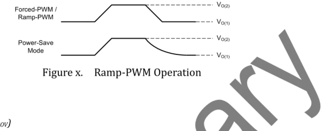
Ramp-PWM Operation (RPWM)If you want the device to operate in power-save mode, but you want to make sure that dynamic voltage scaling
t t
t t
V
ramps the output voltage up and down in a controlled way. Ramp-PWM operation need to be enabled, the device operates in forced-PWM when it ramps from one output voltage to another during dynamic voltage scaling. If the device operates in power-save mode and Ramp-PWM is disabled, the device cannot always control the ramp from a higher output voltage to a lower output voltage, because in power-save mode the device cannot sink current (see Figure x).
To enable Ramp-PWM operation, set the RAMP bit in the Control register to 1. To disable Ramp-PWM operation, clear the RAMP bit in the Control register to 0.
Forced-PWM / Ramp-PWM
Power-Save Mode
Figure x. Ramp-PWM Operation
Protection FunctionsInput Voltage Protection (VINOV)
Under certain operating conditions, current can flow from the output of the device to the input. For example, this can occur during dynamic voltage scaling when the output ramps down to a lower voltage and the VOUT pin sinks current from the output capacitor. Under such conditions, if the voltage source supplying the device cannot sink current, the voltage on the VIN pin can rise uncontrollably.
To make sure the input voltage stays within the permitted range, the device stops switching if the voltage on the VIN pin is greater than 5.7 V. The device automatically starts to switch again when the voltage on the VIN pin is less than 5.7 V.
Current Limit Mode and Overcurrent Protection
The device has a clamp circuit which limits the peak inductor current in the event of an overload. The exact value of the output current during an overload changes with the operating conditions (VI and VO) and the switching mode
(buck, buck-boost, or boost).
Overloads increase the power dissipation in the device, which increases its temperature. If the device becomes too hot, the thermal shutdown function turns off the converter. When the device cools down, the thermal shutdown function automatically turns on the converter again. Thus, under a permanent overload condition, the device can periodically turn on and off, as it cools down and then heats up.
Thermal Shutdown
The device has a thermal shutdown function which turns off the converter if the junction temperature is greater than 155°C. The device automatically turns on the converter again when the junction temperature is less than 135°C.
When the device detects an overtemperature condition, it sets the TSD bit in the Status register to 1. The device clears the TSD bit to 0 if you read the Status register when the junction temperature of the device is less than 135°C.
Power Good
The device has a power-good function which indicates if the output of the DC/DC converter is in regulation or not. The device detects a power-good condition when the output voltage is greater than 95% of its nominal value and detects a power-not-good condition when the output voltage is less than 90% of its nominal value.
V V V V
Load Disconnect
The input is disconnected from the output when the device is shut down. This prevents any current flow from the output to the input or from the input to the output.
Output Discharge
I
2C Interface
Interface Overview
The WD5125C utilizes I2C interface to write / read internal registers. It supports up to 1000Kbps fast mode plus. The 7-bit I2C address is 0x75H.
Data Transactions
Each data transaction is composed of a Start Condition, a number of byte transfers (set by the software) and a Stop Condition to terminate the transaction. Every byte written to the SDA bus must be 8 bits long and is transferred with the most significant bit (MSB) first. After each byte, an Acknowledge signal must follow. Depending upon the state of the R/W bit, two types of data transfer are possible: Slave Receiver Mode (Write Mode) or Slave Transmitter Mode (Read Mode). The following figures provide more information on this process.
S = START condition
P = STOP condition
Device Address = 1110101 (7 bits, MSB first) Register Address = Reg1 – Reg5 address (8 bits) Data = data to read or write (8 bits)
1 = Read command bit
0 = Write command bit A = acknowledge (SDA low) A* = not acknowledge (SDA high)
Register Definition
Register ListSLAVE ADDRESS REGISTER ADDRESS REGISTER NAME FACTORY DEFAULT FUNCTION
0b1110101 0x01 CONTROL 0x00 Control
0b1110101 0x02 STATUS 0x00 Status
0b1110101 0x03 DEVID 0x50 Device ID
0b1110101 0x04 VOUT1 0x3B VOUT1
0b1110101 0x05 VOUT2 0x41 VOUT2
Register Maps
Address Acronym Register
Name
Detail
Bit Field Type Reset Description
0x01
CONTROL Control7 RESERVED R/W 0b Reserved
6 RANGE R/W 0b
This bit selects the output voltage range. 0: Low range (1.800 V to 4.975 V) 1 : High range (2.025 V to 5.200 V)
5 ENABLE R/W 1b This bit controls operation of the converter. 1 : Converter operation enabled
4 OOA R/W 0b
This bit controls the out-of-audio function.
0 : out-of-audio operation disabled
1 : out-of-audio operation enabled
3 FPWM R/W 0b
This bit controls the forced-PWM function.
0 : forced-PWM operation disabled
1 : forced-PWM operation enabled
2 RPWM R/W 0b
This bit controls the ramp-PWM function.
0 : ramp-PWM operation disabled
1 : ramp-PWM operation enabled
1-0 SLEW R/W 00b
These bits control the slew rate of the converter when the output
voltage setting is changed to a new value. 0b = 1 V/ms
1b = 2.5 V/ms 10b = 5 V/ms 11b = 10 V/ms
0x02
STATUS Status7-2 RESERVED R 0b Reserved
1 TSD R 0b
This bit shows the status of the thermal shutdown function.
0 : temperature good
1 : an overtemperature event was detected
0 /PG R 0b
This bit shows the status of the power-good comparator.
Register Maps(continued)
Address Acronym Register
Name
Detail
Bit Field Type Reset Description
0x03
DEVID Device Identity7-4 MANUFACTURER[3:0] R 0101b
These bits identify the device manufacturer.
器件区分唯一编码
3-2 MAJOR[1:0] R 00b
These bits identify the major silicon revision.
电源厂商自定义
1-0 MINOR[1:0] R 00b
These bits identify the minor silicon revision.
电源厂商自定义
0x04
VOUT1 Device Identity7 Reserved R/W 0b Reserved.
6-0 MINOR[1:0] R/W 0111011b
These bits set the output voltage when the VSEL pin is low.
0011111b=2.6V 0111011b=3.3V 1101111=4.6V
Eg.:25mV step,0100000=2.625V
0x05
VOUT2 Device Identity7 Reserved R/W 0b Reserved.
6-0 MINOR[1:0] R/W 0111011b
These bits set the output voltage when the VSEL pin is high.
0011111b=2.6V 1000001=3.45V 1101111=4.6V
PACKAGE OUTLINE DIMENSIONS
CSP-15L
e2
e1
e
b
A
A2
A1
D
E
e
TOP VIEW
SIDE VIEW
BOTTOM VIEW
A3
Symbol Dimensions in Millimeters
Min. Typ. Max.
A 0.51 0.56 0.61
A1 0.19 0.21 0.23
A2 0.32 0.35 0.38
A3 0.025REF
b 0.24 0.26 0.28
D 1.94 1.97 2.00
E 1.14 1.17 1.20
e 0.40BSC
e1 0.80BSC
TAPE AND REEL INFORMATION
Reel Dimensions
Tape Dimensions
Quadrant Assignments For PIN1 Orientation In Tape
W
P1
Q1 Q2
Q4 Q3
Q1 Q2
Q4 Q3
RD Reel Dimension
W Overall width of the carrier tape
P1 Pitch between successive cavity centers Pin1 Pin1 Quadrant
User Direction of Feed
Reel Dimensions
RD
7inch 13inch
8mm 12mm
2mm 4mm 8mm