Memorization Based Low Power FPGA
Design Using Approximate Computing
G.Sangeetha1, Dr.S.Sumathi2,
M.E. VLSI Design, Adhiyamaan College of Engineering, Hosur, TN, India1
Head of Department, Adhiyamaan College of Engineering, Hosur, TN, India2
ABSTRACT VLSI Circuits are increasingly used as the computing platform for fast and energy-efficient execution of recognition, mining, and search applications. Approximate computing is one promising method for achieving energy efficiency. This project presents an approximate computing methodology for VLSI Circuit design, which target approximate processors and arithmetic blocks. This system proposed memoization as a method for approximation on VLSI Circuits, analyzes different architectural and design parameters that should be considered. The proposed design flow leverages on high-level synthesis to enable memoization-based microarchitecture generation, thus also facilitating a HDL-to-register-transfer-level synthesis. When compared with the previous approaches of bit-width truncation and approximate multipliers, memoization-based approximate computation will achieves a significant dynamic power saving with very small area overhead and better power-to-signal noise ratio values for the benchmarks data.
KEYWORDS: Approximate computing, field-programmablegate array (FPGA), high-level synthesis (HLS).
I. INTRODUCTION
Approximate computing has been proposed as an alternative to exact computing for power reduction in embedded computing systems. It assumes that the applications under investigation can tolerate approximate results, and hence, exact computation becomes unnecessary. Some application examples are data-mining, search, analytics, and media processing, which are collectively referred to as the class of recognition, mining, and search (RMS) applications. Approximation can help to reduce the computation efforts, resulting in lower power consumption. In fact, energy efficiency is one of the main driving forces behind approximate computing.
Approximate computing has been studied at different levels, including processors, language design, and ASIC-style computational blocks, such as imprecise adders. However, there has been only a few previous works that investigate approximate computing on VLSI Circuit design as the computing substrate, although it is widely used to accelerate RMS applications. Implementing memoization-based approximate computing on FPGAs faces a number of challenges. Since memoization requires a comparison of input values, the comparison logic and the read–write operations on a block of memory resource will incur additional area overhead, which must be clearly balanced against the power saving. Additional resources like these also present anadditional load on the clock network on the FPGA and may impact the maximum operating frequency of the design if not managed properly. Memoization-based approximate computing is also challenging from an applica-tion perspective. Different comparison measures need to be selected according to the application type in order to achieve the maximal power saving while sacrificing minimal quality.
image-processing applications and common computation kernels with their data sets, we make recommendations regarding selection of proper memoization techniques and comparison measures. The exper-imental results show a significant power saving (around 20%) with small quality degradation.
AIM OF THE PROJECT
This project focuses on developing the automatic synthesis flow to exploit the benefits of memoization for approximate computing. Memoization is a technique that involves reusing a previously computed value for the same input arriving again later and thus skipping repeated computation. In this way, memoization has the potential to improve the performance and save energy by trading computation for a few memory operations. Memoization has been extensively studied for processors, where the focus was on accelerating application execution by reducing the number of required computations by the reuse of the previous stored output. In this paper, we extend the range of output reuse to provide approximation instead. In the simplest case, if two inputs, which are temporally spaced, differ from each other by a small threshold or follow a pattern, then the computed output value of one input can be used as the output for the other input, thus leading to approximation.
Implementing memoization-based approximate computing on VLSI Circuits faces a number of challenges. Since memoization requires a comparison of input values, the comparison logic and the read–write operations on a block of memory resource will incur additional area overhead, which must be clearly balanced against the power saving. Additional resources like these also present an additional load on the clock network on the FPGA and may impact the maximum operating frequency of the design if not managed properly. Memoization-based approximate computing is also challenging from an application perspective. Different comparison measures need to be selected according to the application type in order to achieve the maximal power saving while sacrificing minimal quality.
BLOCK DIAGRAM
OVERVIEW BLOCK DIAGRAM OF PROPOSED SYSTEM PROPOSED SYSTEM OVERVIEW:
In this Project, we analyze memoization-based approximate computing with VLSI Design as the computing substrate from all of the above perspectives. We present and discuss the static memoization and dynamic memoization as well as the comparison measure settings for the applications to benefit from these specific memoization techniques. The nature and the availability of data sets are analyzed, which determines the proper memoization method for a better quality of results. An integrated high-level synthesis (HLS) flow is developed to automatically synthesize the memoization-based design. Based on our experiments using both the image-processing applications and common computation kernels with their data sets, we make recommendations regarding selection of proper memoization techniques and comparison measures.
flow. It shows snippets of code from a C-language source file, where a function denominated edge_detect has been identified for HLS. It additionally shows an example configuration file (config.tcl) which shows the function that has been identified for memoization. The configuration file additionally takes as input other paramount parameters, such as kindred attribute measure, threshold, and so on, which are described in detail in Section IV-A. The source file is first processed by an HLS implement, such as Vivado HLS or LegUp, resulting in the generation of a register transfer level (RTL) descrip-tion called edge_detect.v.
PROPOSED ITERATIVE DESIGN FLOW FOR MEMOIZATION-BASED APPROXIMATE COMPUTING.
We surmise an iterative design flow for memoization-predicated approximate computing. The details of this iterative design flow are shown in proposed iterative design flow. Here, P1 and P2 refer to the potency values obtained without memoization and with memoization, respectively; R1 and R2 refer to the computed values obtained without memoization and with memoization, respectively; P and T are the puissance and result precision thresh-olds, respectively. Proposed iterative design flow shows not only the memoization architecture generation flow but additionally the considerations cognate to power and precision of results that must be considered. The red block shows that an application or task described in C/C++ language is synthesized utilizing an HLS implement.
evaluate the potential power preserving (green block). The potency analysis is performed utilizing the data set corresponding to the application (vigorous or impuissant). The percentage distinction between P1 and P2 should be more preponderant than utilizer-defined threshold P compared with the area overhead due to the wrapper.
The potency dissipation due to the HLS synthesized design (P1) and the potency dissipation due to memoized architecture (P2) are calculated utilizing vendor implements, such as Xilinx Xpower analyzer (XPA) . Simulation results of data set processing, i.e., R1 (plenarily correct result, no approximation) and R2 (approximated result due to memoization), are then compared to visually perceive if their difference is within a utilizer-defined tolerable limit T for precision. If any of these conditions fail, the utilizer needs to adjust the memoization conditions (threshold, homogeneous attribute measure, and so on) for the memoization wrapper engenderer to regenerate another wrapper for evaluation.
A single homogeneous attribute measure will result in just one design for a given power and quality threshold. However, if a designer provides a list of homogeneous attribute measures, the iterative design flow can probe for a more optimized design. With a list of kindred attribute measures, multiple designs satiating a given power and quality threshold will be engendered.A designer can then cull one design among these utilizing power preserving per-unit area (PSPA) metric (defined in Section IV-B) to compare the engendered designs. In integration, the design flow is flexible for a utilizer to set incipient constraints. For instance, if a designer provides a set of puissance thresholds, the iterative design flow will engender multiple designs with different power savings, from which the designer can cull one design.
MEMOIZATION ARCHITECTURE GENERATOR
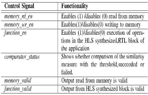
as he/she is more vigilant of the domain of application to which the proposed memoization-predicated approximate computing is being applied. we only provide detailed guidelines to avail that decision making process with veneration to the effect on hardware architecture and power consumption. The paramount control signals of the wrapper are listed in Table I. Here, the recollection_wr_en signal is utilized only in dynamic memoization wrapper, while the others are mundane signals in both the architectures.
II. POWER AND COMPUTATIONAL ACCURACY ANALYSIS
After the memoized architecture generated has been placed and routed on the FPGA device using a vendor specific placement and routing tool (such as Xilinx ISE), its dynamic power analysis is performed using the FPGA vendor tools. Strong data set is used for statically memoized architecture, and weak data set is used for dynamically memoized archi-tecture. The timing simulation of the design after placement and routing provides both the computation results as well as information on switching activity. The switching activity information is used as input to the power analysis tools for the dynamic power analysis. It should be noted here that the static power consumption of an FPGA device is constant irrespective of the design implemented on it. Hence, only dynamic power consumption is of relevance. Such a power analysis is also performed on the base architecture, which is simply the HLS synthesized block without any wrapper. The computation results of the two architectures utilizing the data set are withal compared. If the percentage of potency preserving due to the utilization of memoized architecture and the difference in the precision of the computation results are acceptable, the memoized architecture is substantiated as the final design.
Since the wrapper will integrate extra resource utilization, in order to take this area overhead into consideration, we introduce a supplemental figure of merit called PSPA for evaluating the architecture, as defined in
PSPA = Dynamic Power Preserving/Area Overhead.
The area overhead corresponds to the resources in the FPGA utilized by the wrapper. Such resources include slice flip-flops (FFs), LUTs, and so on. PSPA is expressed in per unit of a resource and calculated for those architectures which have passed tests for power preserving and precision. An archi-tecture that achieves the maximum power preserving with the least area overhead would be regarded as the best candidate. PSPA is proposed as a metric, because it avails in comparing different memoized architectures.
Table I
Important control signal present in the wrapper
III. STATIC MEMORIZATION ARCHITECTURE
An RTL wrapper wraps an HLS synthesized block which implements the computational task. The kindred attribute measure of an input vector with a reference vector is calculated in the kindred attribute measure calculation block inside the RTL wrapper. The result of calculation is then compared with the threshold (Th) in the compare with threshold block and if it lies within the threshold, comparator_status signal is set to be true. Consequently, recollection_rd_en signal is set to be true to enable the recollection address generation. Then, a recollection address corresponding to the output value stored in read only recollection (ROM) for the reference vector is engendered, and the output value can be read out from the ROM. We utilize ROM here since for the static memoization cases, the recollection block is preinitialized with output values according to the offline analysis of the vigorous data set. The inverted version of comparator_status signal drives the function_en signal. When comparator_status is true, func-tion_en becomes erroneous, and as a result, the HLS synthesized block is incapacitated. No computation takes place in this block, and hence, there is no switching activity in this block. Otherwise, when the comparator_status is set to be mendacious as a result of a failed comparison with the threshold, the HLS synthesized block will drive the final output. The latencies of the computation path in the wrapper (beginning from homogeneous attribute measure calculation and ending at the output of ROM) are best matched with the latency of the HLS synthesized block to ascertain that there is zero or least increase in the total delay.
IV. DYNAMIC MEMORIZATION ARCHITECTURE
A RAM block is needed for the dynamic memoization cases, as both indite and read accesses to the recollection resource are needed. The recollection_wr_en signal is engendered only for dynamic memoization wrapper. The memoization wrapper engenderer additionally engenders a counter. The number of count stages that this counter goes through betokens the number of output values to be indited to the RAM block and the number of reference vectors to be stored in reference input set during run time. The step count of the counter denotes the temporal disseverment between the extracted reference values. The step count can be any number depending on the requisites of the particular use-case of the application. For instance, if the step count is 1 and the terminal count is 5, then a total of five output values will be indited to the RAM. In another case, if the step count is 3 and the terminal count is 6, then a total of two output values will be indited to the RAM.
Let us take the case of terminal count equals 5 and step count equals 1 as a detailed example. In this case, the indite_valid signal is set to true for the first five input vectors. These input vectors are indited to the reference input set block. As long as indite_valid is true, the blocks of kindred attribute measure calculation, compared with threshold, and recollection address engenderer (outside red block) are incapacitated. The read port of RAM is withal incapacitated. The HLS synthesized block is enabled and its output drives the final output. The output value is additionally indited to the RAM utilizing the address engendered by recollection address engenderer (inside red block). Thus, the indite port of RAM is enabled as long as indite_valid is true. After the first five input vectors, the indite_valid signal becomes erroneous. Hence, all the blocks inside the red block are incapacitated. Thereafter, the architecture functions like the statically memoized architecture.
For the cases where the step count is not 1, the architecture functions in a more involute way. There is alternative inditing to and reading from the RAM until the counter reaches its terminal count. Let us take an example where the terminal count is 6 and the step count is 2. In this case, input vector arriving at time t = 0, t = 2, t = 4, and t = 6 is stored as reference input vectors, and their output values calculated by the HLS synthesized block are indited to the RAM. At t = 0, indite_valid is true, and hence, the input vector is stored as reference input vector. As discussed in the last example, kindred attribute measure calculation, comparison with threshold and so on, blocks, and read port of RAM are incapacitated. The output of HLS synthesized block is stored. For the input vector at t = 1, indite_valid is set to erroneous, and hence, kindred attribute measure is calculated with veneration to the reference vectors stored until now (which is the input vector at t = 0 in this case). If comparison with threshold prospers, the output value stored in the RAM is read out, else the HLS synthesized block engenders an output by processing the input vector at t = 1. The pattern reiterates until the counter reaches it terminal value. Again, after that, indite_valid is always erroneous, there is no more writing to the RAM and the blocks inside the red box remain disabled without switching activity thereafter.
V. CHOICE OF MEMORY RESOURCES
Both the ROM and the RAM need to be mapped to a recollection resource on the FPGA. The size of the recollection required is predetermined during the static memoization as the output values to be stored are already kenned. On the other hand, this size is resolute utilizing step count and terminal count values together with the output bit width.
The memoization wrapper engenderer automatically utilizes an opportune recollection resource. For up to 128 bits of recollection, the FFs on the FPGA are culled as registers distributed recollection, which is implemented in slice recollection (LUTs configured as recollection), is culled for up to 512 bits, and for more than 512 bits, guidelines are utilized when designs are targeted for Altera FPGAs.
VI. EXPERIMENTAL SETUP AND RESULTS
FPGA contrivance. We report dynamic power preserving, area overhead, and quality of result metrics, such as MSE or power signal-to-noise ratio (PSNR), as per the congruousness to application under investigation.
Table II
MEMOIZATION-BASED DYNAMIC POWER SAVING (AT 100 MHz) F OR REAL SVM APPLICATIONS
VII. CONCLUSION AND FUTURE WORK
We have proposed memoization-predicated approximate computing and applied it to approximate com-puting on FPGAs. A consummate C-to-RTL design flow is with all presented. The results of applying static or dynamic memoiza-tion to commonly used kernels in approximate computing and
investigation, paramount observations were withal made in approximate computing on FPGA.The proposed design methodology is more oriented toward FPGA than ASIC, because it is not possible to utilize ASIC design techniques, such as multiple voltage islands, power gating, and so on, in subsisting FPGAs. In additament, approximate designs of functional units, such as multipliers and targeting ASIC technologies, do not necessar-ily lend well to FPGAs, as shown in this paper. We would relish to note that, in principle, the proposed memoization methodology can withal be applied to the memoization in the ASIC design, where it can be combined with other methods to achieve benefits.
REFERENCES
[1] J. Huang, J. Lach, and G. Robins, “A methodology for energy-quality tradeoff using imprecise hardware,” in Proc. 49th Annu. Design Autom. Conf., 2012, pp. 504–509.
[2] J. Han and M. Orshansky, “Approximate computing: An emerging paradigm for energy-efficient design,” in Proc. 18th IEEE Eur. Test Symp., Avignon, France, May 2013, pp. 1–6.
[3] H. Esmaeilzadeh, A. Sampson, L. Ceze, and D. Burger, “Architecture support for disciplined approximate programming,” in Proc. 17th Int. Conf. ASPLOS, 2012, pp. 301–312.
pp. V. Gupta, D. Mohapatra, S. P. Park, A. Raghunathan, and K. Roy,“IMPACT: Imprecise adders for low-power approximate computing,” in Proc. Int. Symp. Low Power Electron. Design (ISLPED), Aug. 2011,409–414.
[4] K. Shi, D. Boland, and G. A. Constantinides, “Imprecise data-path design: An overclocking approach,” ACM Trans. Reconfigurable Technol. Syst., vol. 8, no. 2, Apr. 2015, Art. ID 6.
[5] D. Citron, D. Feitelson, and L. Rudolph, “Accelerating multi-media processing by implementing memoing in multiplication and division units,” in Proc. 8th Int. Conf. ASPLOS, 1998, pp. 252–261.
[6] F. Khalvati and M. D. Aagaard, “Window memoization: An effi-cient hardware architecture for high-performance image processing,” J. Real-Time Image Process., vol. 5, no. 3, pp. 195–212, Sep. 2010.