ABSTRACT
ZWEBER, AM Y ELIZABETH. Enhancement of the Lithographic Process Using Supercritical Carbon Dioxide in the Development Step. (Under the direction of Dr. Ruben G. Carbonell.)
As microelectronic features reach the 45 nm- node and beyond, extreme ultraviolet (EUV)
lithography and other techniques are being explored as the next generation lithographic
process. The current and continuing challenges faced by these practices are the reduction of
image collapse and line width roughness (LWR). This dissertation covers two techniques
utilizing CO2 in the development step with the means to reduce these challenges: a CO2
drying method to remove the development rinse solution and a carbon dioxide compatible
salt / supercritical carbon dioxide (CCS / scCO2) direct development.
The CO2 drying method uses scCO2 to reduce the surface tension of the water rinse
solution after development. This method has potential to reduce image collapse but not in a
timely manner due to the water solubility in CO2 being too low for chemical removal and yet
too high for mechanical removal.
On the other hand, the CCS / scCO2 direct development of standard EUV photoresists
achieves reduction of both line width roughness and image collapse in high aspect ratio
features. The CCS / scCO2 one step development takes advantage of the scCO2 low surface
tension to help prevent image collapse and the plasticizing properties of CO2 in polymers to
assist in reduction of line width roughness. The CCS, a fluorinated ammonium salt,
associates with the photoresist Brönsted acid groups in the unexposed regions promoting the
photoresist dissolution into the scCO2 rich phase, which results in a reverse development.
A simplified rate model and quartz crystal microbalance (QCM) rate experiments were
the high pressure CCS / scCO2 solution. At 5mM CCS, the zero order photoresist removal
confirmed that the photoresist phase transfer, photoresist mass transfer, or both were the rate
limiting steps which was the premise used for the rate equation. Increasing temperature
(35ºC-50ºC) at a density of 0.896 g/ml was found to increase the removal rate due to phase
transfer limitations and followed an Arrhenius behavio r (Ea = 79.0 kJ/mol). Increasing
pressure (4000-5000 psig) at 40ºC also increased the removal rate due to an increasing CO2
solubility parameter and phase transfer coefficient, but at 50ºC pressure had little effect on
the removal rate where phase transfer limitations were no longer present. When the CCS
concentration was in global excess of Brönsted acid groups 2400:1 at 5mM, the CCS / scCO2
developer removed the photoresist linearly with time. At lower CCS concentrations but still
in global excess of Brönsted acid groups, the photoresist removal slowed (0.5mM CCS,
~240:1) or was prevented (0.03mM CCS, ~15:1) due to partitioning of the CCS between the
CO2 rich phase and the film.
The fundamentals of CO2 and CCS adsorption onto the SiO2 substrate and CO2
absorption into the photoresist film were also investigated using the high pressure QCM at
35°C and 50°C. Adsorption studies of scCO2 were comparable to other flat plate geometry
studies. The adsorption of CCS was found to begin at 8.0 MPa with a temperature of 35°C
and at 9.4 MPa at a temperature of 50°C, where the adsorption of the CCS was driven by
entropy. The absorption of CO2 into the glassy photoresist resin was also measured with
QCM and found comparable to CO2 absorption in glassy polystyrene for 35°C and 50°C.
The diffusion behavior during CO2 absorption was found to be comparable to fluorescent
ii
DEDICATION
BIOGRAPHY
Amy Zweber, formerly Amy Geissler, was born and raised by Irvin and Colleen Geissler
in Bloomington, MN. During her time as an undergraduate at the College of Saint Benedict
in St. Joseph, MN, she spent four months studying abroad in Salzburg, Austria. In 2002, she
graduated with a major in chemistry and minor in mathematics from the College of Saint
Benedic t receiving a Bachelor of Arts degree. In aspirations of a higher degree and warmer
weather, she moved to North Carolina to attend graduate school at North Carolina State
University. In 2004, she married Jeffrey Zweber and received a Master of Science from
North Carolina State University in the Department of Chemical Engineering. In 2007, she
defended this dissertation and received a Doctorate of Philosophy also in the Department of
Chemical Engineering at North Carolina State University. Following graduation, Amy
Zweber will begin her professional career at IBM in Burlington, VT as a Mask Development
iv
ACKNOWLEDGMENTS
The material is based upon work supported by the STC Program of the National Science
Foundation under Agreement No. CHE-9876674. This work was also performed in part at
the Triangle National Lithography Center (a member of the National Nanotechnology
Infrastructure Network) which is supported by the National Science Foundation under
Cooperative Agreement ECS-0335765.
I would like to thank my advisor, Dr. Ruben Carbonell, for the numerous opportunities to
attend and present at conferences and also for guiding me through my research and the PhD
program. I would also like to thank Micell Technologies, Inc. for engaging me in the CCS /
scCO2 development project, and especially Dr. Mark Wagner for his valuable and ongoing
help and discussion. I appreciate the time and effort of the people in the Triangle National
Lithography Center, especially Dave Vellenga, Myrick Peacock, Dr. Ginger Yu, and Joan
O'Sullivan, and also the people in the Analytical Instrumentation Facility, especially Dr. Dale
Batchelor, Chuck Mooney, and Roberto Garcia. I would like to thank the graduate students
in the NSF STC and in the Kenan CO2 center, especially Ke Wang, Yazan Hussain, Mary
Kate Boggiano, Dave Frankowski, Dawei Xu, Alan Chang, and Shaun Tanner, for the ir help
in the laboratory. For their help and support in my core courses, I thank Victoria Wagner and
Alison Julson. I am grateful for the help, encouragement and relief from work provided by
the other graduate students, especially Kristen Comfort, Don Comfort, Julie Willoughby,
Paul Chin, Michael Weiger, Sabrina Tachdjian, Alex Marchet, Josh Michel, Brian Prevo, and
many more. I am indebted and thankful to my husband's family for taking me in as a family
member when I needed them most and to my own family for keeping me involved with the
happenings in Minnesota when I wasn't around and giving me unconditional support and
TABLE OF CONTENTS
Page
LIST OF TABLES ...viii
LIST OF FIGURES ...ix
1. LITHOGRAPHIC PROCESS BACKGROUND AND CHALLENGES ...1
1. 1 Motivation...1
1.2 Lithographic Process Overview...3
1.2.1 Spin Coat...4
1.2.2 Post Applied Bake...5
1.2.3 Exposure...6
1.2.4 Post Exposure Bake ...7
1.2.5 Development ...8
1.2.6 Hard Bake ...8
1.2.7 Etch ...8
1.2.8 Strip ...9
1.2.9 Photoresists ...9
1.3 Current Lithographic Challenge s and Literature Review ...15
1.3.1 Image Collapse...15
1.3.2 Line Width Roughness...19
1.4 Supercritical CO2 in Microelectronics ...21
1.4.1 Properties and Benefits of Supercritical CO2...21
1.4.2 Methods of a scCO2-Modified Development to Reduce Image Collapse and LWR...22
1.5 Conclusions ...27
References ...28
2. CCS / scCO2 DIRECT DEVELOPMENT PROCESS AND CHEMISTRY...33
2.1 Introduction...33
2.2 CCS / scCO2 Development Chemistry ...34
2.3 CCS / scCO2 Development Procedure with QCM as a Dissolution Rate Monitor ...36
2.3.1 Synthesis and Purification of CCS Components ...37
2.3.2 CCS Solution Preparation...37
2.3.3 QCM Apparatus and Measurements ...38
2.3.4 CCS Solution Flush...40
2.3.5 Conversion of Frequency Changes to Mass Changes ...41
2.4 Efficacy of CCS / scCO2 Solution Flush to Displace CO2...42
2.5 Typical Photoresist Removal Experimental Results ...44
2.6 Photoresist Dissolution Reproducibility ...50
vi 2.8 CO2 Drying Step and Adhesive Coating Effect on Photoresist
Development ...54
2.8.1 Photoresist Removal Monitored by QCM ...56
2.8.2 Photoresist Coated Wafer Development ...61
2.10 Conclus ions ...65
References ...66
3. THERMODYNAMICS AND KINETICS OF CCS / scCO2 DEVELOPMENT...69
Abstract ...69
3.1 Introduction...70
3.2 Theory...71
3.3 Materials and Methods...76
3.3.1 CCS Cloud Point Curve Measurement ...76
3.3.2 High Pressure QCM Experiments...77
3.3.3 Determining Photoresist Dissolution Pressure...77
3.4 Results and Discussion ...78
3.4.1 Cloud Point Curve of CCS in CO2 and Photoresist Dissolution Curve in CCS/CO2...78
3.4.2 Temperature Effect on Photoresist Removal Rate ...79
3.4.3 Mass Transfer Effect on Removal Rate ...82
3.4.4 Pressure Effect on Removal Rate...84
3.4.5 CCS Concentration Effect on Removal Rate ...85
3.4.6 Polymer Type Effect on Removal Rate ...91
3.5 Conclusions ...93
References ...94
4. SORPTION OF CO2 AND A CO2 COMPATIBLE SALT ONTO A BARE SIO2 SUBSTRATE AND INTO A PHOTORESIST FILM ...95
Abstract ...95
4.1 Introduction...95
4.2 Materials and Methods...98
4.3 Results and Discussion ...99
4.3.1 CO2 and CO2 / CCS Adsorption onto a Bare SiO2 Substrate ...99
4.3.2 CO2 Absorption into the Photoresist Film ...103
4.3.3 CO2 Diffusion into the Photoresist Film ...105
4.4 Conclusions ...110
References ...111
5. CO2 DRYING AFTER A TRADITIONAL DEVELOPMENT...114
5.1 Introduction...114
5.2 Removing Water Using Dissolution or Mechanical Means ...115
5.2.2 Shear Force Water Removal Model...125
5.3 CO2 Drying Procedure ...128
5.3.1 Processing Lines with Imminent Image Collapse...128
5.3.2 Drying Apparatus ...132
5.3.3 Wafer Processing ...133
5.3.4 Drying Procedure ...135
5.3.5 SEM Analysis ...136
5.4 CO2Drying Results ...137
5.4.1 Image Collapse Reproducibility...137
5.4.2 CO2 Dry and N2 Dry ...141
5.4.3 CO2 Dry and N2 Dry With and Without Helium Displacement ...144
5.5 Conclusions ...148
References ...149
6. CONCLUSIONS...151
APPENDICES ...154
Appendix A...155
Appendix B...158
Appendix C ...160
viii
LIST OF TABLES
Page
Table 2.1 Removal rate reproducibility ...51
Table 3.1 Estimated mass transfer coefficients...73
Table 3.2 Effect of temperature at constant CO2 density on photoresist removal rate...81
Table 3.3 Effect of pressure on photoresist removal rate at 40°C and 50°C ...84
Table 3.4 Effect of CCS concentration on photoresist removal rate ...86
Table 3.5 CCS partition coefficient ...89
Table 3.6 Estimates of the ratio of CCS molecules in the film to photoresist reactive groups ...90
Table 5.1 Peng-Robinson equation of state parameters for carbon dioxide and water...117
LIST OF FIGURES
Page
Figure 1.1 Moore's Law of DRAM ½ pitch features over time as reported by
the ITRS 2005 ...1
Figure 1.2 The lithographic process ...4
Figure 1.3 Effect of spin speed and solvent content on film thickness ...5
Figure 1.4 Geometry pertaining to the numerical aperture of the focusing length ...7
Figure 1.5 Novolac structure ...10
Figure 1.6 DNQ light driven reactio n into an indenecarboxylic acid ...11
Figure 1.7 Difference in dissolution rates of exposed and unexposed novolac photoresist with and without DNQ allows for photoresist contrast...11
Figure 1.8 Acid production from the PAG after exposure followed by acid catalyzed photoresist deprotection during the post exposure bake ...12
Figure 1.9 Examples of photoresists for 248 nm lithography and 193 nm lithography ...13
Figure 1.10 EUV lithography tool prototype ...15
Figure 1.11 Profile and top view examples of image collapse with the EPIC-V41 193nm photoresist...16
Figure 1.12 Schematic of residual rinse solution between photoresist features...17
Figure 1.13 Scanning electron microscope image demonstrating line width roughness in the EPIC-V41 193 nm photoresist ...19
Figure 1.14 CO2 phase diagram...21
Figure 1.15 Methods for using scCO2 in the development step ...23
Figure 1.16 SEM images comparing EUV photoresist patterned with a 130 nm half-pitch...25
x
Figure 2.1 CCS structure ...34
Figure 2.2 CCS reaction with the unexposed photoresist as seen on the top portion allows for photoresist dissolution, and the exposed photoresist as seen on the bottom portion prohibits photoresist dissolution ...35
Figure 2.3 QCM apparatus ...38
Figure 2.4 Mass fraction photoresist removed plotted with the CSTR model...44
Figure 2.5 Example of typical QCM photoresist removal results at 5mM CCS, 50°C, and 34.5 MPa ...45
Figure 2.6 Resistance-Frequency plots...49
Figure 2.7 Removal of photoresist film coated with dip and spin coating methods ...52
Figure 2.8 Removal of photoresist films coated using dip coating ...53
Figure 2.9 Optical microscope images and AFM images showing the bare QCM SiO2 substrate, a dip coated film, and a spin coated film ...54
Figure 2.10 AFM images of a developed QCM substrate with CO2 drying step and a developed pre-coated wafer with HMDS adhesive coating ...56
Figure 2.11 Sample holders used to position the QCM substrate and the silicon wafer vertically in the development cell during the experiment ...56
Figure 2.12 Removal of photoresist with time at 50°C and 34.5 MPa...58
Figure 2.13 AFM images of the photoresist film with varying process conditions of a CO2 drying step and HMDS adhesive coating...62
Figure 2.14 Contour AFM image plots with a 0° pitch and 315° rotation...64
Figure 3.1 Diagram of photoresist development ...76
Figure 3.2 Phase equilibrium analyzer diagram...77
Figure 3.3 CCS in CO2 cloud point and photoresist dissolution point for temperatures 35°C - 50°C ...79
Figure 3.5 Arrhenius plot at constant density (0.896 g/ml)...81
Figure 3.6 Effect of mass transfer on photoresist removal...83
Figure 3.7 Effect of pressure on photoresist removal rate...85
Figure 3.8 Effect of CCS concentration at 50°C and 34.5 MPa...87
Figure 3.9 Example plots at 50°C and 34.5 MPa of low CCS concentration experiments ...88
Figure 3.10 Van't Hoff plot of partition coefficient temperature dependence ...89
Figure 3.11 Photoresist dissolution dependence on CCS concentration within the film...90
Figure 3.12 Comparison of the CCS / scCO2 development of various commercial EUV photoresists ...91
Figure 3.13 Removal of commercial photoresist compared to poly(hydroxystyene) and poly(acrylic acid)...92
Figure 4.1 Schematic depicting sorption experiments in this chapter...97
Figure 4.2 QCM apparatus ...99
Figure 4.3 CO2 adsorption onto the bare SiO2 substrate measured using QCM at 35°C and 50°C ...100
Figure 4.4 Weight gain on the QCM SiO2 surface due to CO2 and CO2 / CCS adsorption at 35°C and 50°C...102
Figure 4.5 Mass of CCS adsorbed as a function of pressure for 35°C and 50°C ...103
Figure 4.6 Comparison of CO2 absorption into polystyrene from the literature to CO2 absorption data into the standard EUV photoresist from this work at 35°C and 50°C ...105
Figure 4.7 Example experimental data used for calculating the diffusion coefficient of CO2 in the photoresist film at 50°C ...106
Figure 4.8 Example plot of M versus −1 t from the data in Figure 4.7 ...107
xii Figure 4.10 Example plot of experimental data from Figure 4.7 and calculated
values of M/M∞ versus t ...108
Figure 4.11 Diffusion coefficients in CO2 swollen polystyrene ...109
Figure 5.1 Surface tension of water in the presence of CO2 at temperatures 30-60oC ...115
Figure 5.2 Amount of water in CO2 plotted as mole fraction and water concentration...116
Figure 5.3 Flat plate geometry used to determine flux of water and IPA into fluid phase by convective force ...118
Figure 5.4 Initial geometry of CO2 flowing over water ...119
Figure 5.5 Effect of pressure on the flux of water/IPA into CO2 (T=40oC and CO2 velocity=0.0211 m/s) ...121
Figure 5.6 Effect of temperature on the flux of water/IPA into CO2 (P=9.7 MPa and CO2 velocity=0.0211 m/s)...122
Figure 5.7 Effect of CO2 velocity on the flux of water/IPA into CO2 (T=40oC and P=9.7 MPa) ...122
Figure 5.8 Convective Diffusion Model with mass transfer coefficients corresponding to laminar, turbulent, and jet flow...123
Figure 5.9 Jet removal of the water/IPA mixture from the high pressure cell using CO2...124
Figure 5.10 Schematic of CO2-rich phase flowing over liquid phase ...125
Figure 5.11 Shear force water removal model at 40oC and 9.7 MPa ...127
Figure 5.12 Test mask layout ...129
Figure 5.13 The critical aspect ratio for which the features will collapse...130
Figure 5.14 The critical aspect ratio is plotted for equal line and space features (l = d = 80nm) and for overexposed features (d = 80nm, l = 100nm) ...131
Figure 5.16 Drying apparatus ...133
Figure 5.17 Wafer matrix for scanner exposure ...134
Figure 5.18 Sample holder ...135
Figure 5.19 Flowchart for conceptual picture of image collapse experiment program...137
Figure 5.20 ICE images show inconsistency in positions on wafer...138
Figure 5.21 Line and space strip and SEM image box size comparison...139
Figure 5.22 SEM images of the positions analyzed for a CO2 dried sample at 110 nm half-pitch...140
Figure 5.23 Percent image collapse as a function of position for three methods of drying 110 nm half-pitch lines and spaces...140
Figure 5.24 Drying with CO2 and N2...142
Figure 5.25 Concentration of water in CO2 and N2 phases at equilibrium for 323K ...144
Figure 5.26 Drying with CO2 and N2 with and without helium displacement ...146
1
C
HAPTER1
Lithographic Process Background and Challenges
1. 1 Motivation
Integrated circuits, or microchips, are used for many of today’s advanced electronic and
communications technology, including computers and cell phones. The integrated circuit
consists of a web of features that are created by a process called lithography, which assemble
and interconnect up to and beyond a million electronic components per chip. Consumer
demand for faster, higher storage devices drives the need to fabricate smaller integrated
circuit features. The precipitous reduction of feature size with time in the microelectronics
industry is often described by Moore’s Law (see Figure 1.1), which predicts that the typical
DRAM 1/2 pitch will decrease from 70 nm today to 45 nm by 2010. This dramatic feature
size reduction has been made possible by continuous improvements in the lithographic
process.
Chapter 1: Lithographic Process Background and Literature Review
Two important issues facing litho graphy users today are the reduction of image collapse
and line width roughness (LWR). These issues will become increasingly problematic for
smaller features, where more stringent tolerances are essential. For example in regards to
LWR, the necessary critical dimension (CD) control for a 70 nm DRAM ½ pitch is 7.4 nm,
while the necessary CD control for a 32 nm DRAM ½ pitch is 3.3 nm. According to the
ITRS 2005 edition, the manufacturable solution for 3.3 nm CD control is not yet known.1
Image collapse and LWR adversely affect device performance and production yield, and thus
solving these problems is of utmost importance to the integrated circuit industry.
Beyond the technical issues of image collapse and LWR, lithography also consumes a
large quantity of solvents and chemicals. According to a study performed in 2002, the
production of a 2-gram 32MB DRAM microchip consumes 1.7 kg of chemicals and fossil
fuels, 32 kg of water, and 0.7 kg of elemental gases.2 In reaction to this concern, the
environmental, health, and safety section of the ITRS 2005 edition suggests reducing waste
from "wet" processes in lithography by further optimization of the current processes.1
The overarching goal of this project was to reduce the challenges resulting from
decreasing feature sizes and excessive material usage by converting the lithographic process
to a "dry" process. Previous work has focused on the synthesis of novel photoresists that are
soluble in both liquid and supercritical CO2, which allows the photoresist to be spin coated
with liquid CO2 and developed with supercritical CO2.3-5 The research for this dissertation
focused on the search for a "dry" process which would eliminate the need for new photoresist
materials and be more easily integrated into the current lithographic process. The objective
was to study the potential use of supercritical carbon dioxide (scCO2) in the development
Chapter 1: Lithographic Process Background and Literature Review
3 This chapter contains an introduction to the lithographic process, a description of how the
current lithographic challenges are being addressed in literature, and a section focusing on
using scCO2 as a means to reduce some of these challenges. The remaining chapters delve
into the results for using scCO2 in the development step using two different techniques. The
first technique is the direct development of a standard photoresist with a scCO2 and CO2
compatible salt (CCS) solution, and the second technique involves developing the photoresist
with a standard solution with subsequent drying using scCO2.
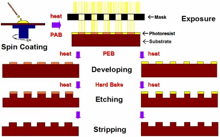
1.2 Lithographic Process Overview
The objective of lithography is to pattern a substrate (i.e., silica) with micro- and
nanostructures, where 25 or more lithographic process repetitions results in complete
fabrication of an integrated circuit.3 Lithography itself is a multi-step process: spin coat, post
applied bake, exposure, post exposure bake, development, hard bake, etch, and strip. (see
Figure 1.2). In this section, each step will be explained to provide a basic understanding of
Chapter 1: Lithographic Process Background and Literature Review
Figure 1.2. The lithographic process: left, negative tone processing; right, positive tone processing.
1.2.1 Spin Coat
In the first step, a uniform layer of a photosensitive polymer (photoresist) is deposited by
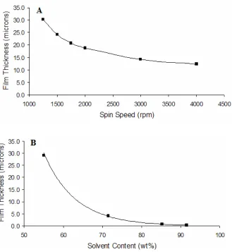
spin coating the material onto the substrate to be patterned. The thickness of the resulting
photoresist film is dependent on the spin speed and the solution viscosity giving the
lithographer control of the film thickness as demonstrated by Figure 1.3. As the spin speed
increases, the film thickness decreases due to centrifugal forces removing photoresist from
the surface before the film dries. As the viscosity decreases, the solution is less restrained
from spreading and the film thickness decreases. In Figure 1.3B, the effect of solution
viscosity on film thickness is represented by diluting the photoresist solution with solvent.
The more dilute solution is less viscous, which results in a thinner film. Typically,
Chapter 1: Lithographic Process Background and Literature Review
5
Figure 1.3. Effect of spin speed and solvent content on film thickness. Graph (A) shows the effect of spin speed on film thickness with the as received propylene glycol monomethyl ether acetate (PGMEA) solvent concentration. Graph (B) shows increasing concentrations of PGMEA or reduced viscosities of the photoresist solution and the film thickness corresponding with those concentrations.
The spin speed was 1300 rpm for 60 seconds. Both studies used thick film AZ50XT photoresist and were post applied baked at 95°C for 90 seconds before measuring the thickness with profilometry.
1.2.2 Post Applied Bake
The residual spin-coating solvent is removed from the photoresist film by heating the
wafer with a hot plate or oven during the post applied bake. The post applied bake raises the
photoresist temperature near its glass transition temperature (Tg), releasing trapped residual
solvent and densifying the photoresist film. This seemingly straightforward step has a strong
Chapter 1: Lithographic Process Background and Literature Review
length of the post applied bake.6-11 Initially, the residual solvent is removed exponentially
and the rate is dependent on the solvent volatility, where higher temperatures remove more
solvent by increasing the solvent volatility. As the film densifies the removal becomes
dependent on solvent mass transfer due to slowing solvent diffusion through the film. In
regards to adjusting the two parameters, the length of the post applied bake only needs to be
long enough to relax the polymer and remove the bulk of the residual solvent. The post
applied bake temperature has two constraints: the temperature must be above the Tg to
maximize the solvent removal and below the degradation temperature. More detail on how
the solvent content and the post applied bake affect the resulting features for specific
photoresist types will be discussed in the photoresist section.
1.2.3 Exposure
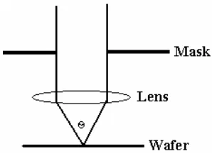
In the next step, the photoresist is exposed to light through a mask that contains the
pattern to be transferred to the wafer. The mask pattern is projected onto the photoresist and
the light creates a chemical reaction in the exposed regions. The smallest obtainable feature
size or resolution
( )
R in lithography is directly proportional to the wavelength of exposurelight
( )
λ and inversely proportional to the numerical aperture of the focusing length( )
NA .12NA k
R= λ
The numerical aperture (NA) is related to the refractive index of the atmosphere that the light
propagates (n) and the angle at which the light is focused onto the wafer (θ) (see Figure 1.4
for geometry).
θ
sin
Chapter 1: Lithographic Process Background and Literature Review
7 As a result, the wavelength of light used in lithography is one of the variables used to reduce
feature size by decreasing over time from 436 nm wavelength to the current 193 nm
wavelength exposure. Initially, the trend of reducing the wavelength of light made 157 nm
lithography appear to be the most logical next step in reducing the smallest possible feature
size, but this proposal was met by a variety of photoresist and exposure tool complications.
Instead, it is expected that future reductions in feature size will be made by increasing the
numerical aperture (NA) using techniques such as immersion lithography or eventually
leaving optical lithography for extreme ultraviolet (EUV) (13nm) lithography.
Figure 1.4. Geometry pertaining to the numerical aperture of the focusing length.
1.2.4 Post Exposure Bake
Following exposure, the wafer is baked in the next step called the post exposure bake.
The post exposure bake temperature is set near the glass transition temperature of the
photoresist to improve diffusion in the polymer resin and to propagate the photosensitive
reaction originally initiated by exposure. Even heat distribution is important to allow for
even diffusion and reaction propagation. During this step, the chemically modified regions
can be visually seen appearing on the photoresist. The chemical reactions occurring in the
photoresist during exposure and the post exposure bake vary from one photoresist to another
Chapter 1: Lithographic Process Background and Literature Review
1.2.5 Development
After the post exposure bake, the exposed regions of the photoresist differ chemically
from the unexposed regions, and a developing solution, commonly 0.26 N
tetramethylammonium hydroxide (TMAH), selectively removes one region, leaving the other
behind. In negative tone development, unexposed photoresist dissolves in the developing
solution and is removed. In positive tone development, the exposed photoresist is soluble in
the aqueous TMAH solution and removed during development. A common development
method is puddle development where a fixed volume is deposited on the wafer and spun off
with a rotating table. Water is used to rinse the remaining developer and is also spun off the
surface. In the experiments presented within this dissertation using the traditional
development, the photoresist is placed in a TMAH bath followed by a water rinse bath to
remove the base from the surface.
1.2.6 Hard Bake
An optional hard bake often follows to drive off residual water from the development
process. The lithographic steps beyond the hard bake were not executed for this research.
The rest of this section briefly explains them for clarity on the entire lithographic process
typically used in integrated circuit processing.
1.2.7 Etch
With the pattern now on the photoresist, the wafer is etched. The photoresist is resistant
to the etching process, so that only the exposed areas of the substrate are etched. The two
types of etching used are the dry and wet etch. The wet etch is more cost effective, but is
Chapter 1: Lithographic Process Background and Literature Review
9 nanometer size features. The components and conditions of each etch vary widely to
accommodate for the variety of substrates and photoresists used in the lithographic process.
1.2.8 Strip
Finally, the remaining photoresist is stripped from the wafer with a stripping solution,
leaving the patterned wafer behind. Stripping solutions are traditio nally a sulfuric acid and
hydrogen peroxide mixture. At this point the patterned wafer is ready for application of
dopants, metals, or other layers befo re repetition of the lithographic process.
1.2.9 Photoresists
The name photoresist comes from its purpose in lithography. The photoresist resin used
must be light sensitive ('photo') and resistant to the etching step ('resist') in order to produce
the desired features in the substrate. A variety of photoresists are available commercially,
which are each tailored to meet specific applications. Some photoresists are used to build
integrated circuits through multiple lithographic steps, while some are used for packaging
purposes and need high aspect ratio holes for electrical contacts. The photoresists ha ve
different chemistries, some which dissolve after being exposed to light (positive tone) and
some dissolve without exposure to light (negative tone). Overall, photoresists need to meet a
few basic requirements. The photoresist must have a built- in chemistry available that upon
exposure to a certain wavelength of light it reacts in such a way to provide contrast upon
development. The photoresist must be transparent to that same wavelength of light, so the
light can propagate through the photoresist material. The photoresist must also be rigid
enough to prevent defects. Finally, the photoresist must have a molecular weight below the
critical entanglement molecular weight, so that dissolution in the development solution is
Chapter 1: Lithographic Process Background and Literature Review
In the next few paragraphs, some typical positive tone photoresists used to make
integrated circuit features in the different feature size nodes will be discussed concerning
their application, chemistry, and basic properties. This explanation of lithography and the
photoresists involved is aimed to give the reader a general understanding of the process.
There are also many other techniques to improve the process, such as addition of a quencher
to the photoresist and use of double patterning, which are not covered here for simplicity.
Micron Size Features: G-line and I-line Lithography
Used mainly for micron sized features, both G- line (436 nm wavelength) and I-line (365
nm wavelength) lithography use novolac resists (see Figure 1.5). The no volac resin by itself
is not photoactive, so a second molecule is needed to provide contrast upon exposure to light.
The photoactive compound used is diazonaphthoquinone (DNQ) (see Figure 1.6). The
contrast in development between exposed and unexposed no volac comes from a difference in
dissolution rates. DNQ acts as a dissolution inhibitor, but after exposure to light the DNQ
photoproduct acts as a dissolution promoter. Thus, the unexposed regions of novolac and
DNQ have a slow dissolution rate in TMAH, while the exposed regions of novolac and the
indenecarboxylic acid photoproduct have a much faster dissolution rate in TMAH (see Figure
1.7).
Chapter 1: Lithographic Process Background and Literature Review
11
Figure 1.6. DNQ light driven reaction into an indenecarboxylic acid.12
Figure 1.7. Difference in dissolution rates of exposed and unexposed novolac photoresist with DNQ allows for photoresist contrast.13
The post applied bake plays an important role in processing thick novolac photoresist
films because it controls the film residual solvent content. In the novolac photoresist, the
DNQ light activated reaction requires water to form the photoproduct carboxylic acid, which
provides the photoresist with contrast. The amount of residual solvent in the film after the
post applied bake can determine how fast the film can hydrate. With thin novolac photoresist
films, film hydration is fast, but with thick photoresist films, the necessary hydration time is
approximately 90 minutes in a cleanroom where the humidity is well monitored. If the
Chapter 1: Lithographic Process Background and Literature Review
form interconnects.14 If the solvent content is too low, the novolac resist cracks or
delaminates under stress15-17 and the photospeed is reduced due to little to no rehydration.14
100 Nanometer to Micron Size Features: Deep Ultraviolet Lithography
Deep ultraviolet (DUV) lithography, which includes 248 nm and 193 nm wavelengths
coming from an excimer light source, is used to make features as small as 100 nm. The light
sources are weaker causing the photoresist resin contrast to be insufficient. A new technique
using chemically amplified resists and a photoacid generator (PAG) was implemented to
increase resist contrast. The chemically amplified polymer resins have protecting groups to
make them insoluble in TMAH. Once exposed to UV light each PAG produces an acid
which reacts with the photoresist to remove the protecting group. (see Figure 1.8) The
removed protecting group then produces another acid group. Since the acid is reproduced in
this catalytic process and can unprotect another polymer segment, the photoresist is
considered chemically amplified. Contrast is possible by the unexposed photoresist
insolubility and the exposed photoresist solubility in the developing solution.
Chapter 1: Lithographic Process Background and Literature Review
13 Poly(hydroxystyrene) is typically used in 248 nm lithography due to its transparency in
248 nm wavelength light, while the photoresist typically used for 193 nm lithography is
poly(acrylic acid). One type of protecting group used for both types of photoresists is the
tertiary-butoxycarbonyl (t-BOC) group. Figure 1.9 shows poly(acrylic acid) and polystyrene
with and without the t- BOC protecting group. Beyond these basic photoresists, variations are
used that include copolymers and blends of these and other polymers.
Figure 1.9. Examples of photoresists for 248 nm lithography and 193 nm lithography. Poly(hydroxystyrene)-type photoresist with t-BOC protecting group shown on left and poly(acrylic
acid)-type photoresist with t -BOC protecting group shown on right.
Residual solvent remaining after the post applied bake affects chemically amplified
photoresist sensitivity and contrast with more intensity than those without chemical
amplification due to acid diffusion. Looking again at the chemistry, remaining solvent in the
film acts as an acid diffusion path facilitating the acid mobility.7, 8 Increasing the post
applied bake temperature or length reduces the residual solvent content and acid diffusion,
which positively affects image contrast. At the same time, the exposure dose required to
create these features (photoresist sensitivity) increases with decreasing solvent content due to
increased photoresist density and inhibition to diffusion.7-10 A compromise must be reached
Chapter 1: Lithographic Process Background and Literature Review
Sub-100 Nanometer Lithography
193 nm lithography can achieve features just below 100 nm, but its ability to make
smaller features is limited. Lithographers attempted to move to 157 nm lithography to
further decrease the wavelength used and improve the possible resolution, but the challenges
met were extreme. Instead the industry has moved to increase the numerical aperture (NA).
The latest technique is 193 nm immersion lithography, where the light propagates through a
median with a higher refractive index than air (n = 1.00) which inc reases the NA. Currently,
water (n = 1.33) is one medium being explored, and exposure tools are being developed to
accommodate for this change.
Once photolithography can not be extended further, extreme ultraviolet (EUV)
lithography is expected to follow. EUV lithography uses 13 nanometer light from a xenon
gas source directed onto a mask and then onto the photoresist coated wafer. Challenges
include producing mirrors which are smooth and reflective enough to provide adequate
exposure to the wafer. Sandia National Laboratories is one location where this idea is being
explored, and Figure 1.10 shows the concept and prototype of the EUV tool being developed.
The photoresist used in EUV lithography is similar to the 248 nm lithography photoresist in
Chapter 1: Lithographic Process Background and Literature Review
15
Figure 1.10. EUV lithography tool prototype. Images taken from Sandia National Laboratories website.
1.3 Current Lithographic Challenges and Literature Review
The lithographic process often needs to be repeated 25 or more times on each wafer to
fabricate a complete integrated circuit.3 Integrated circuit manufacturing is both energy and
material intensive,2 as mentioned previously. In addition to health and environmental
concerns, the use of organic solvents and water poses significant defect related challenges to
the production of the next generation 35 nm features, including image collapse and line width
roughness. In this section, both image collapse and line width roughness are discussed.
1.3.1 Image Collapse
Image collapse is one of the main concerns during the development process using
aqueous solvents. As the aspect ratio of deposited photoresist patterns increases, image
collapse is promoted. Image collapse, which is the deformation of photoresist structures, is
caused by weak adhesion of photoresist to the substrate, the weak structure of the photoresist,
and the high surface tension of the aqueous rinse solution.18, 19 As the rinse solution
evaporates from feature crevices, the surface tension of the remaining rinse solution can pull
Chapter 1: Lithographic Process Background and Literature Review
collapse, the new development process must prevent image collapse for aspect ratios greater
than three, be of relatively low cost, and also be compatible with current development times,
which are about 2-3 minutes, to be attractive to industry.
Figure 1.11. Profile and top view examples of image collapse with the EPIC-V41 193nm photores ist.
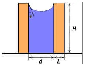
A closer look at the theory behind image collapse helps identify the aspect ratio where
the features will collapse. A beam sway model for the resist feature and the surface tension
acting on it has been used to model the forces responsible for image collapse. The
expressions below describe the aspect ratio (Ac) at which the features will begin to collapse
(see Figur e 1.12 for geometry) :18
For o
90 << θ 3 / 1 2 ) cos(
24
= = θ γH d E L H A c c
For o
90
≈
θ is
3 / 1 2 ) sin(
4
Chapter 1: Lithographic Process Background and Literature Review
17 The parameters used to estimate the critical aspect ratio are the resin critical tensile modulus
(Ec), the distance between the features (d), the fluid surface tension (γ ), the height of the
feature (H), and the contact angle of the fluid on the resist wall (θ ). Looking more closely
at the parameters involved, increasing the strength of photoresist material (Ec) and reducing
the surface tension of the development rinsing solution (γ ) can help prevent image collapse
for high aspect ratio features.
Figure 1.12. Schematic of residual rinse solution between photoresist features.
Enhancing Photoresist Strength
Photocrosslinking the photoresist20 and using blended polymer additives, such as
fullerenes21, are methods that have been used to increase photoresist strength and rigidity.
Tanaka, et al., photocrosslinked photoresist features underwater by flood exposure and dried
the features with nitrogen gas. Flood exposure increases the crosslink density of the
photoresist preventing image collapse. Shibata, et al., blended C60 and C70 fullerenes to
positive tone ZEP520 photoresist.21 Aspect ratios of 5.5 were achieved for a 90 nm pitch
feature with a height of 250 nm, but the approach was expensive. The added cost of
fullerenes per wafer was approximately $28 if 10 weight percent fullerenes were used as
Chapter 1: Lithographic Process Background and Literature Review
Reducing Surface Tension
Tanaka, et al., were some of the first researchers to reach the conclusion that image
collapse occurred during the drying step of development because they observed no image
collapse while the features remained in the rinse solution.18 The authors acted on their
finding by replacing the water rinse with tert-butylalcohol and then freeze-drying to remove
the solvent.22 Freeze-drying lowers the rinse solution surface tension to near-zero, and image
collapse was prevented. Finding the best rinse solution to freeze dry posed problems because
the rinse solution should not damage the resist, the volume change during the freeze-drying
process must be small, and the melting point of the rinse solution must be around room
temperature.22 Instead of freeze-drying, Yamashita chose to use perfluorohexane to rinse
water because of its low surface tension (10 dyne/cm) compared to water (72.8 dyne/cm).23
Aspect ratios of 5.25 were achievable with a ZEP resist, but outermost lines of the pattern
still collapsed. Extra or dummy lines outside of the necessary pattern were the recommended
solution, which hindered efficiency and reduced wafer real estate.
Simply adding surfactants to the aqueous rinse solution also reduces surface tension.
This method could be easily incorporated in a fabrication plant without changing current
equipment. The necessary surfactant concentration to reduce surface tension and the
compatibility with the photoresist have been studied by a variety of groups.24-26 High
concentrations of hydrophobic surfactants can swell and damage the photoresist, while low
surfactant concentrations do not reduce the rinse solution surface tension enough.26 The
reported surfactants that proved harmless to the resist only reduced the surface tension to
Chapter 1: Lithographic Process Background and Literature Review
19 shows that rinsing with the current tested surfactants in water will not completely reduce
image collapse anymore than a less expensive organic solvent.
1.3.2 Line Width Roughness
As features become smaller, the acceptable tolerance for the edge roughness of the lines
decreases (see Figure 1.13). For example, when targeting 70 nm DRAM ½ pitch features,
the tolerated roughness (3σ) for the critical dimensions is 7.4 nm, whereas 32 nm features
have a tolerated roughness of only 3.3 nm.1 The tolerated roughness must be stringent
because it affects device performance and production yield, especially as critical dimensions
decrease.
Figure 1.13. Scanning electron microscope image demonstrating line width roughness in the EPIC-V41 193nm photoresist.
Line width roughness (LWR) and surface roughness are caused by multiple factors,
which makes reducing roughness challenging.28, 29 Reynolds, et al., have categorized the
various factors that affect total roughness assuming each contribution is independent of the
others:27
2 2
2 2
2 2
aerial t
developmen diffusion
shotnoise mask
total σ σ σ σ σ
Chapter 1: Lithographic Process Background and Literature Review
In this approach, the square of the deviation from the mean dimension is viewed as having
contributions from mask deviations, PAG diffusion effects, development errors, and other
factors.
When Re ynolds, et al., examined experimentally the effects of exposure shot noise and
acid diffusion, they noticed that contrary to popular belief, acid diffusion plays a small role in
the overall roughness. They also found that varying post exposure bake temperature and
length had little to no effect on the overall roughness. The main contributions to LWR were
the developer concentration and mask defects. Yoshizawa and Moriya performed a similar
analysis of LWR for e-beam lithography, confirming the conclusions made by Reynolds, et
al.30 In 2002, Houle, et al., also concluded that post exposure bake temperature and length
does not control roughness.28,29 Instead, once the activation energy is met, acid catalysis
has no dependence on the post exposure bake temperature or length.
Two contributing factors absent on Re ynolds’ list are the chemical structure and
polydispersity of the photoresist. In 1993, Yoshimura, et al., found lower photoresist
molecular weight (Mw) and polydispersity (Mw/Mn) resulted in lower photoresist roughness,31
which was confirmed by Narasimhan, et al.32 Another factor Yoshimura, et al., found
contributing to LWR is photoresist rigidity. As the photoresist is developed, more pliable
resist materials are better able to flow and smooth photoresist surfaces, although reducing
photoresist rigidity can also increase image collapse. In general, the chemical structure of the
photoresist has a noticeable effect on LWR.
Overall, both image collapse and LWR are challenges that continually need to be
addressed in lithography as the feature sizes become smaller and aspect ratios become larger.
Chapter 1: Lithographic Process Background and Literature Review
21 or rinse solution surface tension with the goal to reduce image collapse and increase
photoresist pliability for LWR reduction. Both of those goals were achievable using
supercritical CO2 modifications to the development step of lithography.
1.4 Supercritical CO2 in Microelectronics
1.4.1 Properties and Benefits of Supercritical CO2
As a promising solvent, CO2 is currently used in a wide range of industries, such as
polymerization,33,34 dry cleaning,35,36 extractions,37 and pharmaceuticals.38 CO2 has
environmental and economical benefits because it is recyclable, non-toxic, inexpensive, and
nonflammable. When brought into the supercritical region, the density of CO2 is highly
tunable with the ability to reach values close to 1 g/ml, and the CO2 surface energy is near
zero. Beyond high density and low surface tension, supercritical CO2 (scCO2) has a
liquid-like viscosity, while maintaining a gas- liquid-like diffusivity, which can easily be accessed due to
the relatively low critical pressure and temperature (Pc = 7.375 MPa, Tc = 31°C) as seen in
the phase diagram in Figure 1.14.
Chapter 1: Lithographic Process Background and Literature Review
In microelectronics, CO2 has been pursued in the cleaning or stripping,39 spin coating,3, 5
and development4 steps of lithography. Using CO2 specifically in microelectronics has the
valuable potential to replace traditional solvents reduc ing toxicity, the cost of the materials,
and the cost of their disposal.40, 41 Additional to these benefits the ultimate drive for utilizing
scCO2 is based on further improvements to the current microelectronic processes. For
example, the low surface tension, tunable density, and gas- like diffusivity of scCO2 were
employed to improve dirt and scum removal from small crevices between features in
photoresist stripping and cleaning. In this dissertation, these same properties were used in
the development step to reduce image collapse in the high aspect ratio photoresist features.
Reduction of LWR was realized by taking advantage of the ability of CO2 to act as a
plasticizer in the photoresist film, which improved photoresist pliability during development.
The following section focuses on the use of CO2 during the development step found in
literature, and introduces the CO2-modified development techniques used in this dissertation.
1.4.2 Methods of a scCO2-Modified Development to Reduce Image Collapse and LWR
Image collapse results from capillary forces occurring during the development step of
lithography. As explained in the current lithographic challenges section, an aqueous, basic
solution of TMAH develops the patterned features in the photoresist, a water rinse displaces
the TMAH, and the water is dried from the surface during photoresist development. The
surface tension of water tends to pull the features together as it dries within the crevices. At
a critical aspect ratio and spacing, the features will collapse from the surface tension.18, 19
Thus far, a few techniques have been implemented to reduce image collapse by reducing the
Chapter 1: Lithographic Process Background and Literature Review
23 secondary rinse solution22-26 resulting in longer processing times and/or are limited by the
lowest value attainable for the surface tension, which is approximately 20 mN/m.
Supercritical carbon dioxide (scCO2), with properties of low surface tension, low
viscosity, and high density, has the potential to reduce image collapse and LWR in
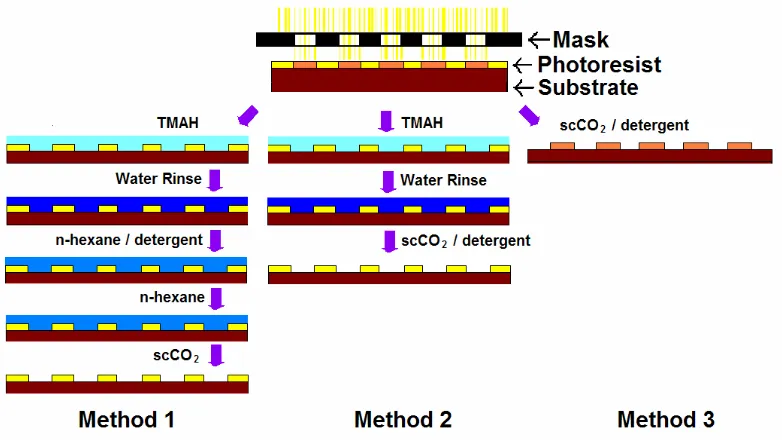
lithography. Three approaches have been examined to use scCO2 in the deve lopment process
(see Figure 1.15). Method 1 and its variants use a CO2-soluble rinsing solution, such as
hexane, to displace water, and then subsequently remove the CO2-soluble rinse solution with
scCO2.42-45 Then, when only pure scCO2 remained in the high pressure development
chamber, the chamber was vented, and image collapse was prevented. The method
successfully reduced image collapse in the photoresist features but also added further solvent
waste, cost, and processing time. Development of only one wafer coupon took longer than
one hour, while traditional development is about 2-3 minutes for a TMAH development,
rinse with water, and spin dry.43
Chapter 1: Lithographic Process Background and Literature Review
A second CO2 drying method was investigated which uses scCO2 to displace the rinse
water directly with the aid of a cosolvent or surfactant (see Figure 1.15, Method 2).46 A
cosolvent or surfactant is necessary for efficient water removal because water solubility in
pure CO2 is low. For example, the solubility of water is only 0.13 weight percent in CO2 at
25oC and 16.5 MPa.47 Zhang, et al., determined water removal using pure CO2 takes
approximately 62 minutes to dry water from a 12x4 mm wafer piece.46 Some of the
surfactants used for this method are fluoroether carboxylate45 and a nonionic methylated
branched hydrocarbon surfactant (TMN-6).46 The total development time when using
fluoroether carboxylate was not reported, and when using TMN-6, 26 minutes was needed.
Incorporating mechanical removal methods Zhang, et al., reduced total development time to
12 minutes by rinsing the wafer coupon with TMN-6 / scCO2, rotating the cell 45o, and
venting.46 Even though the process time was halved, the development time is still four times
longer than traditional development. It is evident that further improvements are necessary
before the semiconductor industry will consider scCO2 development modifications.
However, it is clear from their work that mechanical removal techniques should be examined
more thoroughly to speed up process throughput.
Later investigations in literature led to direct development with a scCO2-based
development solution, which was a more efficient approach to utilizing the beneficial
properties of scCO2 in lithography. Method 3 from Figure 1.15 depicts direct development
with scCO2. Previous work in this area focused on the synthesis and use of novel
photoresists that have been modified to increase their solubility in CO2, usually through
Chapter 1: Lithographic Process Background and Literature Review
25 this area has been limited, however, since the studies used unproven resist systems and
significant improvements in the reduction of pattern collapse were not observed.
Recently, a new technique for the direct development of standard EUV resists with
development times comparable to the standard TMAH process has been reported.52-54 The
process uses a proprietary CO2 compatible salt in homogenous scCO2 (CCS / scCO2) solution
to dissolve the unexposed portions of positive tone EUV photoresists resulting in reverse
image development. Figure 1.16 contains scanning electron microscopy images of a
commercial EUV photoresist developed with TMAH (A), and the same photoresist
developed using the CCS / scCO2 method (B). The photoresist features developed with
TMAH have an aspect ratio of 4.5 and exhibit image collapse, while the photoresist
developed with CCS / scCO2 has features with an aspect ratio of approximately 12 showing
no image collapse. Aspect ratio up to four times greater than TMAH developed features
have been seen using the CCS / scCO2 development method. The CCS / scCO2 technique
takes advantage of the scCO2 properties of low surface tension to reduce image collapse, low
viscosity to develop small features, and high density to dissolve the photoresist.
Figure 1.16. SEM images comparing EUV photoresist patterned with a 130 nm half-pitch. The photoresist was developed with (A) the standard TMAH process (110 nm linewidth) and with (B) CCS
Chapter 1: Lithographic Process Background and Literature Review
In addition to reducing image collapse, the CCS / scCO2 direct development method also
tends to reduce LWR due to the ability of scCO2 to plasticize the polymeric photoresist. In
Figure 1.17, the CCS / scCO2 developed sample is noticeably smoother than the comparable
sample developed in TMAH. Measurement of LWR using a three parameter model
developed by the Institute of Microelectronics (IMEL) has shown an average 30% reduction
in RMS roughness for CCS / scCO2 developed samples versus control samples developed
with standard the TMAH process.55 Multiple factors have been proven to affect LWR,
including resist properties, development conditions, and mask deviations.27, 30 -32, 56-57
Previously proposed remedies to LWR include using surface conditioner solutions after the
development step,58 using a new photoresist with a higher glass transition temperature and
higher transparency,59 and using a new photoresist with a lower molar mass.60 However,
direct development with CCS / scCO2 is a simpler method using commercial EUV
photoresists and developing the resist in a one step process, while reducing both roughness
and image collapse. The CCS / scCO2 direct development mechanism and material properties
Chapter 1: Lithographic Process Background and Literature Review
27
Figure 1.17. SEM images comparing EUV photoresist developed with the standard TMAH process (A, B) and with reverse image development using CCS chemistry in scCO2 (C, D) in which the unexposed
area is removed and the exposed area remains. Images taken by Micell Technologies , Inc.
1.5 Conclusions
The current lithographic process and its challenges have been discussed in this chapter.
As feature sizes decrease, the lithographic process must be reinvented to address the ensuing
challenges. This dissertation explores the use of supercritical CO2 in the development step
using both methods 2 and 3. Method 3 CCS / scCO2 development was the main thrust for
this dissertation due to its fruitful results and potential application to industry. The chemistry
of the CCS and a basic understanding of the CCS / scCO2 development are given in Chapter
2. In Chapter 3, the effects of temperature, mass transfer, pressure, CCS concentration, and
photoresist type on the photoresist removal rate are discussed. In Chapter 4, the CO2 and
CCS sorption behavior on the substrate and in the polymer film, as well as, the CO2 diffusion
into the glassy polymer are explored. Finally, Chapter 5 discusses the attempt to further
reduce the process time of method 2 CO2-modified development, where the final results
show that with the current cell design the time could not be reduced due to the limitations of
Chapter 1: Lithographic Process Background and Literature Review
References
(1) SEMATECH. International Technology Roadmap for Semiconductors. 2005, www.itrs.net/Common/2005ITRS/Home2005.htm.
(2) Williams, E. D.; Ayres, R. U.; Heller, M. Environ. Sci. Technol. 2002, 36, 5504-5510. (3) Hoggan, E. N.; Flowers, D.; Wang, K.; DeSimone, J. M.; Carbonell, R. G. Ind. Eng. Chem. Res. 2004, 43, 2113-2122.
(4) Boggiano, M. K.; DeSimone, J. M. Abs. Amer. Chem. Soc. 2005, 229, U1115-U1116. (5) Hoggan, E. N.; Wang, K.; Flowers, D.; DeSimone, J. M.; Carbonell, R. G. IEEE Sens. J. 2004, 17, 510-516.
(6) Ishii, T.; Matsuda, T. Jap. J. Appl. Phys., Part 2. 1991, 30, L1215-L1217.
(7) Asakawa, K.; Ushirogouchi, T.; Nakase, M. J. Vac. Sci. Technol., B. 1995, 13, 833-839. (8) Itani, T.; Yoshino, H.; Hashimoto, S.; Yamana, M.; Samoto, N.; Kasama, K. Jap. J. Appl. Phys., Part 1. 1996, 35, 6501-6505.
(9) Raptis, I. Jap. J. Appl. Phys., Part 1. 1997, 36, 6562-6571. (10) Raptis, I. Jap. J. Appl. Phys., Part 1. 2001, 40, 5310-5311.
(11) Mack, C. A.; Mueller, K. E.; Gardiner, A. B.; Sagan, J. P.; Dammel, R. R.; Willson, C.
G. J. Vac. Sci. Technol., B. 1998, 16, 3779-3783.
(12) Levinson, H. J. Principles of Lithography. SPIE Press: Washington, 2001. (13) Henderson, C. L., Integrated Circuits: A Brief History;
http://dot.che.gatech.edu/henderson/Introductions/microlithography%20intro.htm.
(14) Dammel, R. R. interview. 2005, February.
Chapter 1: Lithographic Process Background and Literature Review
29 (16) Lei, H.; Francis, L. F.; Gerberich, W. W.; Scriven, L. E. AIChE J. 2002, 48, 437-451. (17) Lei, H.; Payne, J. A.; McCormick, A. V.; Francis, L. F.; Gerberich, W. W.; Scriven, L.
E. J. Appl. Polym. Sci. 2001, 81, 1000-1013.
(18) Tanaka, T.; Morigami, M.; Atoda, N. Jap. J. Appl. Phys., Part 1. 1993, 32, 6059-6064. (19) Namatsu, H.; Kurihara, K.; Nagase, M.; Iwadate, K.; Murase, K. Appl. Phys. Lett. 1995,
66, 2655-2657.
(20) Tanaka, T.; Morigami, M.; Oizumi, H.; Ogawa, T.; Uchino, S. Jap. J. Appl. Phys., Part 2. 1994, 33, L1803-L1805.
(21) Shibata, T.; Ishii, T.; Nozawa, H.; Tamamura, T. Jap. J. Appl. Phys., Part 1. 1997, 36, 7642-7645.
(22) Tanaka, T.; Morigami, M.; Oizumi, H.; Ogawa, T. Jap. J. Appl. Phys., Part 1. 1993, 32, 5813-5814.
(23) Yamashita, Y. Jap. J. Appl. Phys., Part 1. 1996, 35, 2385-2386. (24) Shin, K. S.; Lee, G. J. Photopolym. Sci. Technol. 2003, 16, 363-367.
(25) Jung, M. H.; Kim, H. W.; Lee, S. H.; Woo, S. G.; Cho, H. K.; Han, W. S. J. Photopolym. Sci. Technol. 2003, 16, 463-466.
(26) Tanaka, K.; Yamada, Y.; Masuda, S.; Kobayashi, M.; Kim, W. K.; Anyadiegwu, C.;
Padmanaban, M.; Dammel, R. R. J. Photopolym. Sci. Technol. 2004, 17, 527-534. (27) Reynolds, G. W.; Taylor, J. W. J. Vac. Sci. Technol., B. 1999, 17, 334-344.
(28) Hinsberg, W. D.; Houle, F. A.; Sanchez, M. I.; Wallraff, G. M. IBM J. Res. Dev. 2001,
45, 667-679.
Chapter 1: Lithographic Process Background and Literature Review
(30) Yoshizawa, M.; Moriya, S. J. Vac. Sci. Technol., B. 2000, 18, 3105-3110.
(31) Yoshimura, T.; Shiraishi, H.; Yamamoto, J.; Okazaki, S. Jap. J. Appl. Phys. 1993, 32, 6065-6070.
(32) Narasimhan, B.; Wanat, S. F.; Rahman, M. D. Polym. Eng. Sci. 2000, 40, 2251-2261. (33) Desimone, J. M.; Guan, Z.; Elsbernd, C. S. Science. 1992, 257, 945-947.
(34) Desimone, J. M.; Maury, E. E.; Menceloglu, Y. Z.; McClain, J. B.; Romack, T. J.;
Combes, J. R. Science. 1994, 265, 356-359.
(35) McClain, J. B.; Betts, D. E.; Canelas, D. A.; Samulski, E. T.; DeSimone, J. M.;
Londono, J. D.; Cochran, H. D.; Wignall, G. D.; ChilluraMartino, D.; Triolo, R. Science. 1996, 274, 2049-2052.
(36) DeSimone, J. M.; Romack, T. J.; Betts, D. E.; McClain, J. B. US Pat. 5,944,996. 1999. (37) McHugh, M.; Krukonis, V. Supercritical Fluid Extraction: Principles and Practice. Butterworths: Boston, 1996.
(38) Cocero, M. J.; Ferrero, S. J. Supercrit. Fluids. 2002, 22, 237-245.
(39) Supercritical Fluid Cleaning: Fundamentals, Technology and Applications. Noyes Publications: Westwood, New Jersey, 1998.
(40) Jones, C. A.; Zweber, A.; DeYoung, J. P.; McClain, J. B.; Carbonell, R.; DeSimone, J.
M. Crit. Rev. Solid State Mater. Sci. 2004, 29, 97-109.
(41) Weibel, G. L.; Ober, C. K. Microelectron. Eng. 2003, 65, 145-152.
(42) Namatsu, H.; Yamazaki, K.; Kurihara, K. Micoelectron. Eng. 1999, 46, 129-132. (43) Goldfarb, D. L.; de Pablo, J. J.; Nealey, P. F.; Simons, J. P.; Moreau, W. M.;
Angelopoulos, M. J. Vac. Sci. Technol., B. 2000, 18, 3313-3317.
Chapter 1: Lithographic Process Background and Literature Review
31 (45) Namatsu, H. J. Vac. Sci. Technol., B. 2000, 18, 3308-3312.
(46) Zhang, X. G.; Pham, J. Q.; Ryza, N.; Green, P. F.; Johnston, K. P. J. Vac. Sci. Technol., B. 2004, 22, 818-825.
(47) Weibe, R. Chem. Rev. 1941, 29, 475.
(48) Pham, V. Q.; Rao, N.; Ober, C. K. J. Supercrit. Fluids. 2004, 31, 323-328.
(49) Sundararajan, N.; Yang, S.; Ogino, K.; Valiyaveettil, S.; Wang, J. G.; Zhou, X. Y.;
Ober, C. K.; Obendorf, S. K.; Allen, R. D. Chem. Mater. 2000, 12, 41-48.
(50) Pham, V. Q.; Weibel, G. L.; Nguyen, P. T.; Ferris, R. J.; Ober, C. K. Abs. Am. Chem. Society. 2002, 224, U469-U469.
(51) Pham, V. Q.; Ferris, R. J.; Hamad, A.; Ober, C. K. Chem. Mater. 2003, 15, 4893-4895. (52) Wagner, M.; DeYoung, J.; Harbinson, C. Proc. SPIE. 2006, 6153, 61533W.
(53) Wagner, M.; DeYoung, J.; Harbinson, C.; Miles, M. Proc. SPIE. 2006, 6153, 615346. (54) DeYoung, J.; Wagner, M.; Harbinson, C.; Miles, M.; Zweber, A. E.; Carbonell, R. G.
Proc. SPIE. 2006, 6153, 615345.
(55) Constantoudis, V.; Gogolides, E.; Patsis, G. P.; Wagner, M.; DeYoung, J.; Harbinson,
C. Proc. SPIE. 2006, 6153, 61533W-1.
(56) Eder-Kapl, S.; Loeschner, H.; Zeininger, M.; Fallmann, W.; Kirch, O.; Patsis, G. P.;
Constantoudis, V.; Gogolides, E. Microelectron. Eng. 2004, 73-74, 252-258.
(57) Ma, Y. S.; Tsvid, G.; Cerrina, F. J. Vac. Sci. Technol., B. 2003, 21, 3124-3130.
(58) Zhang, P.; Jaramillo, M., Jr.; Rao, M. B.; Ross, B.; Horvath, B.; Wong, P.; Gehoel, W.;
Sinkwitz, S. Proc. SPIE. 2005, 5753, 1018-1023.
(59) Somervell, M. H.; Fryer, D. S.; Osborn, B.; Patterson, K.; Cho, S.; Byers, J.; Wilson, C.
Chapter 1: Lithographic Process Background and Literature Review
(60) Chang, S. W.; Yang, D.; Dai, J.; Felix, N.; Bratton, D.; Tsuchiya, K.; Kewark, Y.;
33
C
HAPTER2
CCS / scCO
2Direct Development Process and Chemistry
2.1 Introduction
The most efficient way to implement low surface tension scCO2 in the development step
is to use scCO2 directly as the developer. As discussed in Chapter 1, direct development with
scCO2 requires the photoresist material to be soluble in scCO2 either before or after exposure
with acceptable contrast and sensitivity, which usually entails synthesis of a new fluorinated
photoresist material. Recently a CO2 compatible salt (CCS) has been synthesized, which
allows standard commercial EUV photoresists to be developed directly in the CCS / scCO2
solution.1-5 CCS / scCO2 direct development not only reduces image collapse and LWR but
eliminates the use of a traditional tetramethylammonium hydroxide (TMAH) developer and
is compatible with existing standard photoresists.
The development of the photoresist with the CCS / scCO2 developing solution relies on
the selective reaction of the CCS, a fluorinated ammonium salt shown in Figure 2.1, with the
unexposed photoresist to produce high contrast features. The chemistry of this process
involves the reaction of the CCS with the photoresist rendering it soluble in CO2. Without
the CCS-photoresist reaction, the photoresist is insoluble in CO2. This chapter explains the
chemistry occurring during the process and then delves into the procedure used for
Chapter 2: CCS / scCO2 Direct Development Process and Chemistry
Figure 2.1. CCS structure.
2.2 CCS / scCO2 Development Chemistry
The CCS / scCO2 development is both a reactive and diffusive process, involving the
same general four steps as TMAH development: 1) diffusion of the CCS from the bulk
developer solution to the polymer/solution interface and into the polymer, 2) reaction of the
CCS with the photoresist acidic groups, 3) dissolution of reacted photoresist, and 4) diffusion
of the dissolved photoresist into the bulk development solution. The fundamental reactive
step in the CCS / scCO2 process is the association of the CO2 soluble cation of CCS with
unprotected Brönsted acid groups in the resist. In Figure 2.2, the simplified, unexposed
photoresist depicted on the top left consists of protected and unprotected polymer pendant
groups as well as a photoacid generator (PAG). When the photoresist is developed with the
CCS / scCO2 developing solution, the CCS interacts with the Brönsted acid groups in the
polymer backbone to modify the photoresist and enable solubility in CO2. In the regions
exposed to light shown on the bottom left of Figure 2.2, the photoacid generator cleaves the
protecting groups and leaves excess acid in the film. During the CCS / scCO2 development,
the CCS-photoresist reaction is no longer favored due to Le Chatelier's principle, which
renders the resist insoluble in CO2. The high level of contrast and reverse image
development observed in CCS / scCO2 development is believed to be due to this inhibition of
Chapter 2: CCS / scCO2 Direct Development Process and Chemistry
35