ABSTRACT
YANG, LIYU. Techniques to Improve the Performance of Wide Operation Range DC-DC Converters. (Under the direction of Dr. Alex Q. Huang.)
Techniques to Improve the Performance of Wide Operation Range DC-DC Converters
by Liyu Yang
A dissertation submitted to the Graduate Faculty of North Carolina State University
in partial fulfillment of the requirements for the Degree of
Doctor of Philosophy
Electrical Engineering
Raleigh, North Carolina 2010
APPROVED BY:
_______________________________ ______________________________
Dr. Alex Q. Huang Dr. Mesut Baran
Committee Chair
DEDICATION
To my parents
Chaoyu Yang and Shanzhen Li
BIOGRAPHY
ACKNOWLEDGMENTS
I would like to thank my advisor, Dr. Alex Q. Huang, for his continuous support and encouragement to my research and study in North Carolina State University. He provided me the opportunity to explore diverse areas in power electronics and power management IC design. With his inspiration, I can choose the topic that I feel most interested in and conduct research. His guidance led me through the numerous challenges in research. Without his support and guidance, it would not be possible for me to complete this dissertation.
I am very grateful to my other committee members, Dr. Mesut Baran, Dr. Subhashish Bhattacharya and Dr. Srdjan Lukic for their comments and suggestions during the course of this work. Also I would like to thank Dr. Tao Xie to serve as the Graduate School Representative of my defense.
I would also like to thank my colleague students who have helped with discussions and experimental assistance over the years: Dr. Xiaoming Duan, Dr. Jinseok Park, Mr. Ding Li, Dr. Xiaojun Xu, Mr. Ning Zhu, Mr. Hongtao Mu, Dr. Jiwei Fan, Mr. Xin Zhou, Mr. Sungkeun Lim, Mrs. Rong Guo, Mr. Xiaopeng Wang, Mr. Jifeng Qin, Mr. Pochih Lin, Mrs. Jingzhen Hu, Mr. Gaurav Bawa, Mr. Anand Ramamurthy, Dr. Chong Han, Dr. Bin Chen, Dr. Wenchao Song, Mr. Zhaoning Yang, Dr. Yu Liu, Mr. Tiefu Zhao, Mr. Shoubhik Doss, Mrs. Zhengping Xi, Mr. Xiaohu Zhou, Mr. Jun Li, Mr. Sameer Mundkur Mr. Zhigang Liang, Mr. Qian Chen, Mr. Yu Du, Mr. Gangyao Wang, Dr. Yan Gao, Dr. Jun Wang, Dr. Jeesung Jung, Mr. Woongje Sung, Mr. Edward van Brunt, Dr. Jinsang Kim and Ms. Juming Lai.
I appreciate the assistance from the Staff members of SPEC and FREEDM Center, especially Mr. Anousone Sibounheuang, Mrs. Colleen Reid and Mr. Seth Crossno.
TABLE OF CONTENTS
LIST OF TABLES ………...viii
LIST OF FIGURES ………ix
Chapter 1 . Introduction ...1
1.1. Introduction and motivation...1
1.2. Organization of this dissertation ...6
Chapter 2 . Adaptive PWM ramp slope for Buck converters with the spread spectrum function and the input voltage feed-forward function ...8
2.1. Introduction to the input voltage feed-forward function ...8
2.2. Introduction to the spread spectrum function ...10
2.3. Practical circuit to implement the spread spectrum and the input voltage feed-forward functions...14
2.4. The solution to the problem of the spread spectrum function ...19
2.5. Summary of Chapter 2...23
Chapter 3 . Adaptive external ramp for peak current mode controlled Buck converters with wide operation range...24
3.1. Introduction...24
3.2. Theoretical derivation ...28
3.3 Verification with SIMPLIS...42
3.4. Experimental verification ...44
3.5. Summary of Chapter 3...49
4.2. Introduction to the AVP function ...54
4.3. Controller design for phase shedding Buck converters with active droop AVP ....58
4.4. Controller design for phase shedding Buck converters with PCM controlled AVP ...77
4.5. Summary of Chapter 4...85
Chapter 5 . Adaptive device size to improve the light load efficiency of regulated charge pump converters...86
5.1. Introduction...86
5.2. Power stage design...88
5.3. Design of the error amplifier ...99
5.4. Use adaptive device size method to improve light load efficiency ...102
5.5. Transistor level simulation result...110
5.6. Experimental verification with PCB prototype ...112
5.7. Summary of Chapter 5...117
Chapter 6 . Conclusions and future work...119
6.1. Conclusions...119
6.2. Future work...120
LIST OF TABLES
Table 1-1 Operation range of some commercial DC-DC converters ...2 Table 3-1 Working conditions of the eight operation corners ...30 Table 3-2 Transient response comparison between the adaptive Se control method and the
fixed Se control method...49 Table 4-1 Specification of the demonstration board of phase shedding Buck controller
LIST OF FIGURES
Figure 2-1 Circuit diagram of a voltage mode control Buck converter with Vin
feed-forward...9 Figure 2-2 Basic ramp generation circuit...10 Figure 2-3 Large output voltage variation caused by the spread spectrum function ...12 Figure 2-4 Practical circuit implementation of the spread spectrum and the input voltage
feed-forward functions...14 Figure 2-5 Large output voltage variation when the spread spectrum function is enabled
in the practical clock and ramp generation circuit ...16 Figure 2-6 Simulation waveform showing the problem for Buck converters with input
feed-forward when enabling the spread spectrum function...18 Figure 2-7 Using additional current sources to implement the adaptive PWM ramp slope
...20 Figure 2-8 Theoretical waveform to implement adaptive slope for the PWM ramp with
the additional current source method...21 Figure 2-9 Simulation waveform with solution to the problem for Buck converters with
input feed-forward when enabling the spread spectrum function...22 Figure 3-1 Circuit diagram of a peak current mode controlled Buck converter...26 Figure 3-2 Small signal model of a peak current mode controlled Buck converter in CCM
Figure 3-6 Bode plot of the first term of Gvc(s) with fixed external ramp...34
Figure 3-7 Bode plot of the second term of Gvc(s) with fixed external ramp ...35
Figure 3-8 Bode plot of the second term of Gvc(s) with adaptive external ramp...38
Figure 3-9 Bode plot of the first term of Gvc(s) with adaptive external ramp ...39
Figure 3-10 Bode plot of the Gvc(s) with adaptive external ramp ...40
Figure 3-11 Bode plot of the loop gain curves with adaptive external ramp...41
Figure 3-12 Bode plot of the loop gain curves with adaptive external ramp, zoomed in to 10kHz - 100kHz...42
Figure 3-13 SIMPLIS simulation circuit with adaptive external ramp control ...43
Figure 3-14 Loop gain comparison between the small signal model (red dashed line) and the SIMPLIS simulation (blue solid line) ...44
Figure 3-15 Photo of the demonstration board with adaptive external ramp control ...45
Figure 3-16 Steady state operation waveform at Vin=6V, Vo=1.2V, Io=5A ...46
Figure 3-17 Steady state operation waveform at Vin=24V, Vo=5V, Io=0.5A ...46
Figure 3-18 Load transient test waveforms for the adaptive external ramp method ...48
Figure 3-19 Load transient test waveforms for the fixed external ramp method...48
Figure 4-1 Multi-phase Buck converter...52
Figure 4-2 Phase shedding...53
Figure 4-3 Output characteristic of the AVP function...54
Figure 4-4 Equivalent circuit for converters with the AVP function...55
Figure 4-7 Small-signal block of a Buck converter with AVP function using active droop method...59 Figure 4-8 Simulation of AVP function using active droop without phase shedding ...61 Figure 4-9 Simulation of AVP function using active droop with phase shedding ...62 Figure 4-10 Simulation of AVP function using active droop with phase shedding and
modified compensator...65 Figure 4-11 Transfer functions of Buck converter with active droop AVP --- 4-phase
power stage withAv conventional_ ...66 Figure 4-12 Transfer functions of Buck converter with active droop AVP --- 2-phase
power stage withAv conventional_ ...67 Figure 4-13 Transfer functions of Buck converter with active droop AVP --- 2-phase
power stage withAv_ modified...67 Figure 4-14 Photo of the demonstration board for phase shedding Buck converter with
active droop AVP...69 Figure 4-15 Test waveforms of phase shedding Buck converter with active droop AVP,
no phase shedding, Av conventional_ ...70 Figure 4-16 Test waveforms of phase shedding Buck converter with active droop AVP,
with phase shedding, Av conventional_ ...71 Figure 4-17 Test waveforms of phase shedding Buck converter with active droop AVP,
with phase shedding, Av_ modified. ...72 Figure 4-18 Close loop output impedance magnitude with 2-phase compensator and
Figure 4-19 Close loop output impedance magnitude with 1-phase compensator and different number of active phases ...73 Figure 4-20 Simulation waveform of 1-phase compensator design for phase shedding
Buck with active droop AVP, load change between 0A and 30A (between 1-phase and 2-phase) ...74 Figure 4-21 Simulation waveform of 1-phase compensator design for phase shedding
Buck with active droop AVP, load change between 30A and 80A (between 2-phase and 4-phase) ...75 Figure 4-22 Simulation waveform of 1-phase compensator design for phase shedding
Buck with active droop AVP, load change between 0A and 80A (between 1-phase and 4-phase) ...75 Figure 4-23 Loop gain T2 magnitude with 1-phase compensator and different number of
active phases ...76 Figure 4-24 Circuit diagram of a Buck converter with AVP function using peak current
mode control ...77 Figure 4-25 Small-signal block of a Buck converter with AVP function using peak
current mode control ...78 Figure 4-26 Load transient simulation of a four-phase PCM Buck converter with AVP,
constant Ri, without phase shedding. ...80 Figure 4-27 Load transient simulation of a four-phase PCM Buck converter with AVP,
constant Ri, with phase shedding ...81 Figure 4-28 Load transient simulation of a four-phase PCM Buck converter with AVP,
Figure 4-29 Control loop transfer functions for phase shedding Buck converter with PCM
control, constant Ri, without phase shedding...83
Figure 4-30 Control loop transfer functions for phase shedding Buck converter with PCM control, constant Ri, with phase shedding...84
Figure 4-31 Control loop transfer functions for phase shedding Buck converter with PCM control, adaptive Ri, with phase shedding...85
Figure 5-1 IRU3039 evaluation board ...86
Figure 5-2 TPS60255 EVM board...87
Figure 5-3 Power stage of the regulated multi-mode charge pump converter...89
Figure 5-4 The charge pump’s operation in (4/3)x mode ...90
Figure 5-5 The charge pump’s operation in (3/2)x mode ...92
Figure 5-6 The charge pump’s operation in 2x mode...93
Figure 5-7 Simplified equivalent circuit for 2x mode operation in the first half switching period ...96
Figure 5-8 Simplified equivalent circuit for 2x mode operation in the second half switching period...96
Figure 5-9 Using the error amplifier to control the gate of MN1 ...100
Figure 5-10 Simplified schematic of the error amplifier ...101
Figure 5-11 Light load efficiency improvement method --- adaptive device size...103
Figure 5-12 Using a Sense FET to sense the current in MN1 to determine light load condition ...105
Figure 5-13 Current sensing circuit ...107
Figure 5-16 Time domain waveform at Vin=2.7V and Iload=500mA. (From top to bottom:
MN1 current, Vin, Vout and C3 voltage.)...111
Figure 5-17 Transistor-level simulation result of the multi-mode charge pump efficiency ...112
Figure 5-18 Photo of the demonstration board for the multi-mode charge pump with discrete devices ...113
Figure 5-19 Steady state operation waveform at Vin=2.8V (2x mode)...114
Figure 5-20 Steady state operation waveform at Vin=3.6V ((3/2)x mode)...115
Figure 5-21 Steady state operation waveform at Vin=4.5V ((4/3)x mode)...115
Figure 5-22 Experimental efficiency curves at full load ...116
Chapter 1 . Introduction
1.1. Introduction and motivation
The DC-DC converter is one of most common types of electric power converters. It takes a DC source, either regulated or unregulated, as input, and provides one or more DC voltages at the output. In most cases, the output is regulated. DC-DC converters are used everywhere in people’s daily lives and in many industries.
A lot of DC-DC converters need to work with a wide operation range. Some of them have regulated input and output voltages, while the output load current has a wide range. Examples are the voltage regulators for the CPU of computers. Some of them have unregulated input as well. Examples are those using batteries as input. Some of them have an even wider operation range for their input voltage, output voltage, and load current. A lot of commercial DC-DC controllers or converters have the ability to work with this kind of wide operation range. Some of these converters are listed in Table 1-1.
Table 1-1 Operation range of some commercial DC-DC converters
Commercial DC-DC converters
Vin Vout Iout
TPS54362 3.6-48V 0.9-18V 0-3A MAX8655 7-28V 0.7-12V 0-25A
LT3972 3.6-33V 0.79-30V 0-3.5A LM22674 4.5-42V 1.285-5V 0-0.5A
LT3493 3.6-36V 0.78-12V 0-1.2A
Some of the common desirable performance for DC-DC converters can be listed here: good efficiency for heavy load and light load, fast transient response or high control band width, easy compensation design or even integrated compensator, and low Electro-Magnetic Interference (EMI).
When the operation range is wide, it is challenging for people to obtain the above performance because of two major reasons. Firstly, when the operation range is wide, the power stage working condition of the DC-DC converter has a big variation. In other words, the control plant for the compensator design has a big variation, which makes it difficult to design a single compensator to obtain good control performance over the entire operation range.
Secondly, a good technique to improve one part of the performance can be bad for another part of the performance. For example, for higher control bandwidth, the switching frequency needs to be high, but this is not desirable in an efficiency point of view. For example, if the compensator is integrated and fixed, it is difficult to obtain a high bandwidth for all the operating conditions. Another example is that the devices with small on-state resistance are good for heavy load efficiency. But normally they have large gate capacitance too, which is not good for light load efficiency.
For DC-DC converters with a wide load range, people were mainly focusing on the full load efficiency. The reason is that the full load efficiency determines the maximum loss and heat, and therefore the size of the heatsink, and the power density. However, the light load efficiency is becoming a more and more important specification as well. This is especially true in the case of battery-powered applications. The light load efficiency determines the time duration that a battery-powered equipment can stay in the standby mode. To improve the light load efficiency, the method of burst mode is widely used in DC-DC converters nowadays [ 4 ]. Under the burst mode operation, the output of the DC-DC converter is compared with a preset threshold that is less than the nominal output voltage. When the light load condition is detected, the DC-DC converter stops switching and no energy is delivered from the input. So the output is drained by the load slowly. When it reaches that threshold voltage, the DC-DC converter is enabled again, and delivers a certain amount of energy to the output and pulls the output voltage high again. The amount of energy being delivered is determined by a preset timer or by comparison to another preset upper threshold. After that, if the load is still light, the DC-DC converter will enter the burst mode again.
(20Hz-20kHz) and cause an unpleasant noise. Secondly, the output voltage ripple is enlarged in the burst mode operation.
Phase shedding is another way to improve the light load efficiency ( [ 1 ] - [ 2 ] and [ 5 ] - [ 8 ] ). It is applied to the multi-phase converters only. When the light load condition is detected or a command is sent from the load, some phases can be shut down to save the switching loss and the driving loss. Previous literature has shown significant improvements for light load efficiency. However, very few papers have talked about the effect of phase shedding on the compensator design and the transient response of converters with adaptive voltage positioning (AVP) control.
Based on the above discussion, many techniques have been proposed to improve the performance of wide operation range DC-DC converters. However, there are still some topics which require more research, and more novel techniques can be proposed to further improve the performance of wide operation DC-DC converters. This dissertation moves forward along this path, and its contents are organized as shown in Section 1.2.
1.2. Organization of this dissertation
In Chapter 2, it is revealed that the output voltage of DC-DC converters can have a large variation if the spread spectrum function is enabled. The reason is analyzed, and a solution is proposed based on derived analytical equations. The transistor-level simulation verifies that the proposed adaptive PWM ramp slope control can effectively fix this problem, and it is easy to implement in common IC processes. Moreover, the proposed clock and ramp generation circuit integrates both of the spread spectrum function and the input voltage feed-forward function. Very little literature has reported this feature before.
In Chapter 3, a novel adaptive external ramp method is proposed for peak current mode controlled Buck converters with a wide operation range. Assuming one fixed compensator design, the proposed method can significantly improve the bandwidth and the transient response speed compared to a fixed external ramp design.
responses can happen if the controller design is based on the previous guidelines only. The reasons are analyzed, and the solutions are proposed and verified experimentally.
In Chapter 5, the design of a regulated multi-mode charge pump converter is presented. To meet the specifications of the wide input range and the load current range, the sizes of the PMOS and NMOS devices need to be large, which causes the light load efficiency to be low. An adaptive device size method is proposed to be used for the regulated charge pump in this chapter. The simulation and experimental results show that this method can improve the light load efficiency significantly.
Chapter
2
. Adaptive PWM ramp slope for Buck
converters with the spread spectrum function and the
input voltage feed-forward function
2.1. Introduction to the input voltage feed-forward function
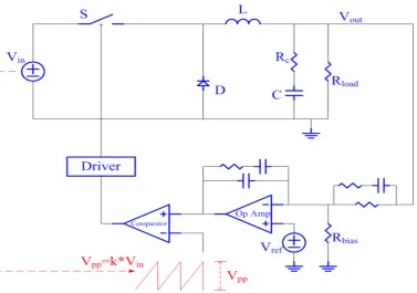
The input voltage feed-forward function is a technique that is widely used for wide operation range Buck converters with voltage mode control [ 9 ] - [ 12 ]. For these Buck converters, if the Pulse Width Modulation (PWM) ramp amplitude is self-adjusted to be proportional to the input voltage Vin, theoretically the bandwidth is approximately the same for all Vin ranges. Therefore, one single compensator is good for all Vin ranges. Also, the impact of input voltage change to output voltage is minimized. One example is the LM22674 from National Semiconductor, which is a monolithic Buck converter with an internal fixed type III compensator and Vin feed-forward. Figure 2-1 shows the circuit diagram of this technique.
The loop gain can be expressed in (2. 1).
1 2
2
1 2
0
1 (1 / )(1 / )
1 ( ) ( )
(1 / )(1 / )
( ) /
c I Z Z
m vd comp in
pp P P
sR C s s
T F G s G s V
V s s s s
where 2 0 2 0 ( )s s s
Q
, 0 1
LC
and
0
1 1
/ c
Q
L R R C
.
As can be seen from (2. 1), if Vpp=k*Vin, the expression of loop gain T is almost the same
for all Vin values.
Figure 2-1 Circuit diagram of a voltage mode control Buck converter with Vin feed-forward
Figure 2-2 Basic ramp generation circuit
However, the basic ramp generation circuit in Figure 2-2 does not have the input voltage feed-forward function. To implement this function, the current source needs to be a voltage-controlled-current-source. Its value needs to be proportional to the input voltage.
2.2. Introduction to the spread spectrum function
In many applications such as in the automotive and medical environments, there are Electro-Magnetic Interference (EMI) regulations or standards that are published and enforced. The DC-DC converters need to meet these standards before they are allowed to be installed.
One of theses techniques is the spread spectrum function [ 15 ] - [ 23 ]. The switching frequency of the DC-DC converter is modulated around the nominal value with a certain pattern. The modulation scheme can be fixed, random, or pseudo-random. For example, if the nominal switching frequency is 2MHz, with this spread spectrum function enabled, the switching frequency can be modulated to 1.9MHz for 10 switching cycles, and then modulated to 2.1MHz for another 10 switching cycles, and then returns to 2MHz for 10 switching cycles. The number of the steps and the duration of each step can be varied to achieve the desired result of EMI noise peak reduction. Many papers have shown that this technique is quite effective in reducing the peak values of the EMI noise generated by the DC-DC converter.
As pointed out in [ 18 ] - [ 23 ], when the spread spectrum function is implemented, the output voltage variation of the DC-DC converter can be increased. One of the main causes of this problem can be illustrated in Figure 2-3.
spectrum mechanism, the rate to change the switching frequency is better to be greater than 20kHz. If the rate of the switching frequency change is too fast for the feedback control and Vc to follow, the output voltage can have a large variation as shown in Figure 2-3. Apparently, to minimize the output voltage variation caused by this mechanism, the PWM ramp amplitude needs to be constant even when the spread spectrum function is enabled.
Figure 2-3 Large output voltage variation caused by the spread spectrum function
feed-forward function requires the PWM ramp amplitude to increase proportionally as the input voltage increases. But, when the input voltage is constant, even if the spread spectrum function is enabled, the PWM ramp amplitude needs to be constant to minimize the output voltage variation.
Some applications, such as automotive applications, have a wide range of input voltage. Therefore, the input voltage feed-forward function is preferred when the voltage mode Buck converter is used. At the same time, many of these applications prefer low EMI. So, it is a desirable feature if these two functions can be integrated together. Unfortunately, very little literature can be found to propose a solution to include both of these two functions. Looking at the commercial DC-DC controllers or converters, very few of them integrate these two functions together in the same controller. The LM3370 from National Semiconductor is one of these very few commercial products. However, the spread spectrum range for LM3370 is 20kHz, which is only 1% of the 2MHz switching frequency. Therefore, even if the clock and ramp generation circuits still follow the basic design, the output voltage variation is not significant. Also, very little information about its clock and ramp generation circuit design is available to the public. [ 18 ] presents a method of spread spectrum for a Buck converter TPS40200 which has an input voltage feed-forward function. However, this implementation is not part of the internal circuits of TPS40200, and an external signal generator is needed.
without a large output voltage variation. The transistor-level simulation verifies the proper function of this solution.
2.3. Practical circuit to implement the spread spectrum and the
input voltage feed-forward functions
A practical circuit implementation for both the spread spectrum and the input voltage feed-forward function is shown in Figure 2-4 [ 10 ].
In Figure 2-4, all the components are inside the controller IC except the resistor ROSC for setting the switching frequency.
The amplifier at the left side applies a voltage that is proportional to the input voltage (k*Vin) across the resistor ROSC, and generates a reference current of Ir. This current is mirrored into two branches, where one branch of the mirrored currents (n*Ir) will generate the PWM ramp, whose amplitude is proportional to the input voltage, by charging and periodically resetting the voltage of CRAMP. This is how the input voltage feed-forward function is realized.
Another branch of the mirrored current (Ir) is applied to the capacitor COSC. The generated ramp is compared to a reference signal REFmod and determines the clock frequency. The value of REFmod is proportional to the input voltage as well. By doing that, once the switching frequency is determined by ROSC, both the amplitude of the clock ramp and the charging current for COSC will change their values simultaneously if the input voltage changes its value, so the switching frequency can be kept the same with the input voltage feed-forward function implemented.
As mentioned earlier in this chapter, a Buck converter can have a large output voltage variation when the spread spectrum function is enabled. The circuit in Figure 2-4 also has this problem. The theoretical waveform of this clock and ramp generation circuit is illustrated in Figure 2-5.
When the spread spectrum function is enabled, the value of REFmod voltage is modulated, therefore the ramp for the clock has a corresponding amplitude change and the frequency of the clock is modulated. However, the amplitude of the PWM ramp VRAMP is correspondingly changed too. The reason is that the charging current for the capacitor CRAMP is still the same for a fixed input voltage but the charging time is different.
To keep the same output voltage Vout, the duty cycle of the Buck converter needs to be constant for a certain input voltage. Because the PWM ramp amplitude is changing, the error amplifier output voltage Vc needs to be changed accordingly to maintain the same duty cycle. There is always some delay for the error amplifier output voltage to respond, so it causes a large output voltage variation.
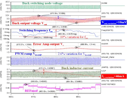
The above analysis can be verified by the transistor-level simulation waveform shown in Figure 2-6. The simulation waveform is obtained by CADENCE simulation of a 2MHz voltage mode Buck converter with a 10V input voltage, a 3.3V output voltage, and a 500mA load current. The power stage components’ models are ideal, but the circuit used to implement the input voltage feed-forward function and the spread spectrum function is a transistor-level circuit in a BiCMOS process.
has a 61mV peak to peak ripple voltage. Subtracting the 13mV ripple voltage under normal operation, the output variation is 48mV. The inductor current has a 495mA peak-to-peak ripple current. Subtracting the 254mA ripple under normal operation, the inductor current variation is 241mA. Both of these variations are undesirable and should be minimized.
2.4. The solution to the problem of the spread spectrum function
From the above analysis, the fundamental reason for the problem of the spread spectrum is the amplitude variation of the PWM ramp. The question is how to maintain the same amplitude for the PWM ramp even when the spread spectrum function is enabled. Since the time duration for the PWM ramp is changing when the spread spectrum function is enabled, the question is translated to how to obtain an adaptive slope for the PWM ramp so that its amplitude can be kept constant.
Based on the above analysis, there are three solutions to the problem. The first one is to adaptively change the capacitance value of CRAMP. But this method is not easy or not cost effective in IC processes. The second one is to adaptively change the charging current for CRAMP. This can be implemented by adding or subtracting current from the nominal charging current of n*Ir. The last solution is to use an adaptive gain stage to correct the variation of the PWM ramp amplitude. It is theoretically possible, but because the falling edge of the PWM ramp is so sharp, this adaptive gain stage needs to have extremely high bandwidth, which is very difficult to be implemented.
Figure 2-7 Using additional current sources to implement the adaptive PWM ramp slope
Figure 2-8 Theoretical waveform to implement adaptive slope for the PWM ramp with the additional current source method
The equation for the PWM ramp amplitude is shown below.
0 1
1
( ) ( )
r additional
RAM P SW
RA M P
r additional O SC X
IN
RA M P r X
n I I
V T
C
n I I C R R R
k V
C I R R
(2.2)
As long as the product of (n I r Iadditional) and 0 1 1
( X )
X
R R R
R R
are kept the same, the
The theoretical waveform with this improvement method is shown in Figure 2-8, and the transistor-level simulation waveform is shown in Figure 2-9 under the same condition as that of Figure 2-6. The switching frequency is still modulated with a 10% variation, but, because of the proposed adaptive slope control for the PWM ramp, the variation of the PWM ramp is reduced to 2.6%. The error amplifier output does not need to change much to keep the same duty cycle. So, the output voltage variation and the inductor current variation are reduced significantly (by ~5 times) to 10mV and 46mA, respectively.
2.5. Summary of Chapter 2
Chapter 3 . Adaptive external ramp for peak current
mode controlled Buck converters with wide operation
range
3.1. Introduction
Buck converters with a wide operation range are frequently seen. For example, TI’s product TPS54362 has an input range from 3.6V to 48V, an output range from 0.9V to 18V, and an output current of up to 3A. Maxim’s product MAX8655 has an input range from 7V to 28V, an output range from 0.7V to 12V, and an output current of up to 25A.
However, sometimes it is preferable to use one fixed compensator to fit a wide operation range. If a DC-DC controller is designed with a fixed compensator, it is easier for the end users since they don’t need to go through the calculation, simulation, and bench tuning process. Another advantage is that the resistors and the capacitors in the compensator can possibly be monolithically integrated into the controller IC. By doing so, the controller IC can use less pins, less external resistors and capacitors, and therefore save the PCB area. The DC-DC converter can be designed with a more compact layout. One example of such a controller is the LT3493 from Linear Tech, which is a peak current mode controlled Buck converter with an internal compensator.
Some control methods have been proposed to design one fixed compensator for wide operation range DC-DC converters. One example is the input voltage feed-forward method mentioned in Chapter 2 for voltage mode Buck converters with a wide Vin range. Since the bandwidth is almost the same for all input voltages if the ramp amplitude is self-adjusted to be proportional to Vin, then one single compensator is good for the whole Vin range.
sensing gain, and the output voltage feed-forward gain, respectively. The term He(s) is from the sample-and-hold effect.
Figure 3-1 Circuit diagram of a peak current mode controlled Buck converter
voltage. It is not clear whether this mechanism is optimum for the application where one single fixed compensator works for a wide range of output voltage. The paper [ 27 ] also discusses a method to improve the bandwidth of peak-current controlled voltage regulators by selecting a suitable external ramp. But the analysis is also for the application of well-defined input voltage and output voltage.
Figure 3-2 Small signal model of a peak current mode controlled Buck converter in CCM
3.2. Theoretical derivation
To design a single fixed compensator for a DC-DC converter with a wide operation range,
one needs to look at the control to output transfer functions
c o vc v
v s
G ( )ˆ ˆ for all working
conditions. Based on the small signal mode in Figure 3-2, the G svc( )function for a PCM
Buck converter can be derived as in (3.1) [ 24 ].
ˆ ( ) 1
( ) ( ) ( )
ˆ 1 ( ) ( ) r ( ) 1 ( 0.5)
m
o vd
vc p h
s
c id m i e vd m i
c
G s F
v R
G s F s F s
R T
v G s F R H s k G s F R m D
L ( 3.1)
where ( ) RC
in
RC L
vd
Z
Z Z
G s V
, ( ) in 1
RC L
id Z Z
G s V
, 1
1/ 1/( 1/( ))
RC
c
Z
R R s C
, ZL s L ,
1
( )
m
e n s
F
S S T
, 2 i r s R k L f
, 2 2
2 ( )
( ) 1
s s e s s f f H s
1
1 /
( ) c
p p sCR s F s , 1 ( 0.5) s p c T m D CR LC
, 1 e
c
n
S m
S
, 2 2
1
1 /( ) /
( )
n n
h s Q s
F s
, n
s T
and
1
( c 0.5)
Q
m D
.
A fixed external ramp of Se=Ri*(Vo,max/L)=50mV/us is used to ensure no sub-harmonic oscillation for all working conditions. The G svc( ) Bode plots in Figure 3-3 covers the
eight corners of the wide operation range as listed in Table 3-1 below.
Table 3-1 Working conditions of the eight operation corners
Trace 1 Trace 2 Trace 3 Trace 4 Trace 5 Trace 6 Trace 7 Trace 8
Vin (V) 24 24 24 24 6 6 6 6
Vo (V) 5 5 1.2 1.2 5 5 1.2 1.2
Io (A) 5 0.5 5 0.5 5 0.5 5 0.5
If the G svc( ) for each case is identical or similar to each other, it will be very easy to
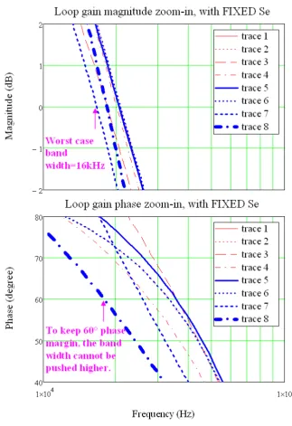
design a single fixed compensator and obtain good control performance over the wide operation range. However, as can be seen from Figure 3-3, there is quite a lot of difference between these curves. Some conventional design guidelines recommend the bandwidth to be 0.1*fsw to 0.2*fsw for Buck converters. If we look at this frequency range (20kHz to 40kHz) in Figure 3-3, the difference in the magnitude is 2dB to 5dB, while the difference in the phase is 20 to 30 degrees. This variation is a limiting factor in obtaining high control bandwidth using a single fixed compensator.
As pointed out in [ 32 ], if the ESR zero is not sufficiently lower than the switching frequency, the loop gain of the PCM Buck converter needs to have at least a 60 degrees phase margin to obtain an optimum load transient response. To ensure that the loop gain for all working conditions has at least a 60 degrees phase margin, a fixed compensator
2650 1 / 2000 1 /1000000 ( ) comp s G s s
s
is used. The compensation zero is placed close to the
dominant pole p, while the compensation pole is placed at the frequency of the ESR
The Bode plots in Figure 3-4 are the loop gain T curves, where TG s Gvc( ) * comp( )s , while
Figure 3-5 is the same set of curves but they are zoomed in to 10kHz-100kHz to illustrate at least a 60 degrees phase margin for all loop gains.
The bandwidth cannot be pushed higher, otherwise the phase margin will be less than 60 degrees for the working condition of Vin=6V, Vo=1.2V and Io=0.5A (trace 8, high-lighted with thicker traces in Figure 3-5).
As can be seen from Figure 3-5, the worst case bandwidth is 16kHz (trace 7, Vin=6V, Vo=1.2V, Io=5A), which is only about 1/12 of the switching frequency. If the external ramp can be adjusted automatically instead of fixed, can it improve the control bandwidth?
If the external ramp Se can be adjusted, it means 1 e c
n S m
S
can be changed. Based on
Equation (3.1) , changing mc will affect the G svc( ) function in three aspects: the DC gain
1
1 s ( 0.5)
i
c
R
R T
R m D
L
, the pole frequency 1 s ( 0.5)
p c
T
m D
CR LC
for F sp( ), and
the quality factor 1
( c 0.5)
Q
m D
for F sh( ) . To see these three effects, the
approximated G svc( ) function in (3.1) can be separated into two terms as listed in (3.2)
and (3.3)
_ _
1 ( )
1 /
1 ( ) 1
1 ( 0.5) 1 ( 0.5)
c vc first term
p p s s i i c c sCR G s s
R F s R
R T R T
R m D R m D
L L
( 3.2)
_ sec _ 2
2
1 ( )
1 ( )
vc ond term
n n
h
s
s s
Q
G F s
( 3.3)
effects on the big variation in G svc( ). The first term is plotted in Figure 3-6. In the
intended crossover frequency range (0.1*fsw to 0.2*fsw), we can see that all the
_ _ ( ) vc first term
G s curves have only negligible variation in terms of magnitude, while the
variation in phase is about 10 to18 degrees.
But, as can be seen from Figure 3-7, in the intended crossover frequency range (0.1*fsw to 0.2*fsw), the Gvc_ second term_ ( )s in Equation (3.3) has about 2 to 4dB variation in magnitude
and 19 to 22 degrees variation in phase using fixed external ramp Se. The variation of the second term is more significant than that of the first term.
As mentioned before, a big variation in magnitude and phase of the G svc( ) transfer
functions means there will be difficulty in designing one fixed compensator for high bandwidth. The question is how to eliminate the variation. The variation in the first term
_ _ ( ) vc first term
G s shows up almost only in the phase, which is mainly determined by the
frequency of the pole 1 s ( 0.5)
p c
T
m D
CR LC
of F sp( ). Once the output capacitor is
calculated and selected, this pole is mainly determined by the load resistanceR, which is normally a design specification instead of a design option. So it is not something that can be controlled by the designer.
However, the designer can have more choice in designing the second term Gvc_ second term_ ( )s .
By observing Equation (3.3), noticing that n
s T
is the same for all cases, if the quality
factor Q can be designed in such a way that it is the same for all working conditions, the
variation for the second term can be eliminated. Therefore, the external ramp Se should be
adaptive such that 1 ( c 0.5)
Q
m D
is a constant, which means m Dc should be a
constant. According to [ 28 ], Q should be less than 1 to ensure the current loop won’t
oscillate. On the other hand, if Q is too small, the external ramp Se is much larger than
the sensed current ramp Sn. The control loop will behave more like voltage mode control instead of current mode control, and the advantages of current mode control is lost. A
Se by using a voltage-controlled-current-source to charge a capacitor and to reset its voltage at the beginning of each cycle. This seems to reach the same implementation as that in [ 25 ]. But, different from [ 25 ], to make Se proportional to Vo is not the only
choice to minimize G svc( ) variation. As long as Q can be kept the same for all operating
conditions, the variation of Gvc_ second term_ ( )s can be eliminated. Q can be other values instead of 2 / , but it is more difficult to implement.
With this adaptive Se control scheme, the second term Gvc_ second term_ ( )s will be the same for
all working conditions as shown in Figure 3-8.
Figure 3-9 Bode plot of the first term of Gvc(s) with adaptive external ramp
With the adaptive external ramp control scheme, the big variation in G svc( )is reduced in
Figure 3-10 Bode plot of the Gvc(s) with adaptive external ramp
Because the variation of G svc( ) is reduced, it allows a new compensator
_
4290 1 / 2000 1 /1000000
( ) comp new
s G
s s
s
to be used while keeping at least a 60 degrees phase
Figure 3-11 Bode plot of the loop gain curves with adaptive external ramp
Figure 3-12 Bode plot of the loop gain curves with adaptive external ramp, zoomed in to 10kHz - 100kHz
The above analysis is verified using the SIMPLIS software, which has been considered as a powerful tool in recent years to verify transfer functions of switch mode power supplies. The reason is that it can obtain transfer functions directly from time domain simulation without using the average models. The simulation circuit is shown in Figure 3-13.
Figure 3-13 SIMPLIS simulation circuit with adaptive external ramp control
Figure 3-14 Loop gain comparison between the small signal model (red dashed line) and the SIMPLIS simulation (blue solid line)
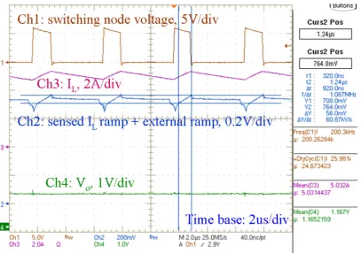
To show the advantage of the proposed adaptive external ramp control, a demonstration board has been built and tested on the bench with the same wide operation range mentioned in Section 3.2: Vin=6V-24V, Vo=1.2V-5V, Io=0.5A-5A, fsw=200kHz, C=100uF, Rc=10mΩ, L=10uH, and current sense gain Ri=0.1V/A. Figure 3-15 shows a photo for this PCB board. The control loop is fixed for the whole operation range except the value of a resistor Rbias connected between the inverting input of the error amplifier and the circuit ground for setting different Vo. The amplitude of the external ramp is automatically controlled by the circuit itself to extend the control bandwidth.
Figure 3-15 Photo of the demonstration board with adaptive external ramp control
The steady state operation waveforms in Figure 3-16 and Figure 3-17 demonstrate that the controller with the adaptive external ramp can work stably for a wide operating range with the proposed automatically self-adjusted external ramp method.
The channel 2 waveforms, sum of the sensed current waveform and the adaptive external ramp, in Figure 3-16 and Figure 3-17, deserve more explanation. To avoid adding more parasitic components to the loop composed of the top switch, the bottom switch, and the input capacitor, the current sensing is done for the inductor current [ 33 ] instead of the top switch current. So both the rising slope Sn and the falling slope Sf are added to the external ramp Se. With the choice of Q2 / , the external ramp Se is automatically
equal to the negative value of the falling slope Sf. So, during the time of bottom switch conduction (D’·T), the external ramp Se and the down slope Sf cancel out, and the channel 2 waveforms in Figure 3-16 and Figure 3-17 are flat during D’·T. During the time of top switch conduction (D·T), the channel 2 waveform should be the sum of the rising slope Sn and the external ramp Se. As indicated by the cursor measurement results shown on the right side of each waveform, the summation slopes are 60.87kV/s and 240.7kV/s, respectively, which are very close to the theoretical values of 60kV/s and 240kV/s. The external ramp capacitor’s voltage is reset at both the rising edge and the falling edge of the PWM signal.
To compare the load transient response, the two compensators 2650 1 / 2000
1 /1000000 ( ) comp s G s s
s
and _ 4290 1 / 2000
1 /1000000 ( ) comp new s G s s
s
are implemented
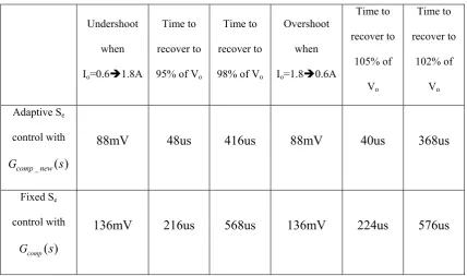
The load transient test results for the case of Vin=6V, Vo=1.2V and Io=0.6A1.8A with the adaptive Se control scheme is shown in Figure 3-18, while the test result with the fixed Se control is shown in Figure 3-19. Based on these two figures and the measurement results comparison listed in Table 3-2, the adaptive external ramp control scheme has a better transient response because of its higher control bandwidth.
Table 3-2 Transient response comparison between the adaptive Se control method and the fixed Se
control method
Undershoot
when
Io=0.61.8A
Time to
recover to
95% of Vo
Time to
recover to
98% of Vo
Overshoot
when
Io=1.80.6A
Time to recover to 105% of Vo Time to recover to 102% of Vo
Adaptive Se
control with
_ ( )
comp new
G s
88mV 48us 416us 88mV 40us 368us
Fixed Se
control with
( ) comp
G s
136mV 216us 568us 136mV 224us 576us
3.5. Summary of Chapter 3
shows that the Q of the second term of Gvc( )s needs to be identical in order to make
( ) vc
G s more similar to each other for wide operation range PCM Buck converters. By
Chapter 4 . Controller design issues and solutions for
Buck converters with phase shedding and AVP
In this chapter, the controller design issues and solutions for multi-phase Buck converters with phase shedding and AVP functions will be discussed.
4.1. Introduction to the phase shedding function
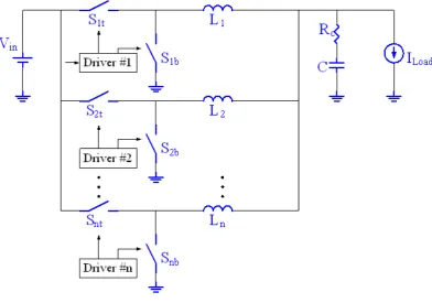
Many applications require the DC-DC converter to deliver a large amount of current to the load. One example is the Voltage Regulator (VR) for computer processors. The recent design guidelines for the VR asks for a 100A or more current to be delivered to the CPU [ 1 ]. For such a high output current application, it is neither practical nor optimal to use a single-phase Buck converter because the power loss generated from the devices is too much.
The circuit diagram of a multi-phase Buck converter is shown in Figure 4-1. The driving signal for each phase is shifted and equally distributed within a switching cycle.
Figure 4-1 Multi-phase Buck converter
The CPU or similar loads can remain in the idle state or other light load state for a long time. In the light load condition, the conduction loss is not significant, but the switching loss and the driving loss are still high due to the afore-mentioned reasons. It causes the light load efficiency to be poor.
As mentioned before, the light load efficiency is becoming a more and more important specification for many DC-DC converters. For a multi-phase converter to improve the light load efficiency, one method is to shut down some phases during the light load condition. This function is called phase shedding. The idea can be seen in Figure 4-2.
Many papers ([ 1 ] -[ 2 ] and [ 5 ] - [ 8 ]) have shown theoretical and experimental data to demonstrate that the light load efficiency can be improved significantly with phase shedding.
4.2. Introduction to the AVP function
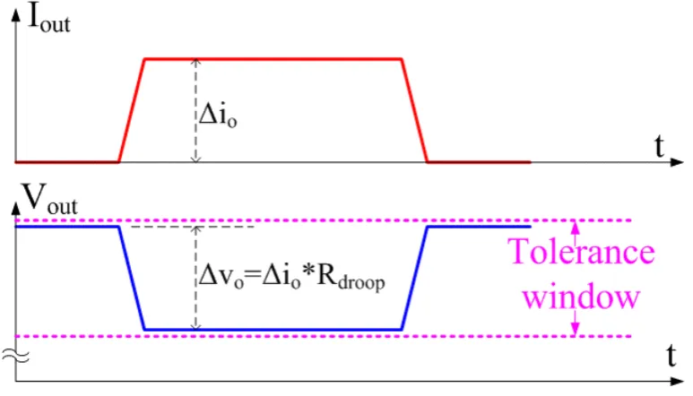
There are two types of characteristics for the output regulation of the DC-DC converters. The first type of characteristic tries to regulate the output voltage to a defined voltage, no matter what the load current is. The second type is called Adaptive Voltage Positioning (AVP). The characteristic is shown in Figure 4-3.
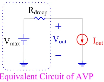
For the AVP characteristic, the output voltage is not intended to be regulated at a fixed voltage regardless of the output current. Instead, the output voltage is dependant upon the output current. More specifically, the output voltage is regulated to be a little lower than the upper limit of the tolerance window at no load, and a little higher than the lower limit of the tolerance window at full load. Therefore, the equivalent circuit of the Buck converter with the AVP output characteristic is an ideal voltage source Vmax in series with a load-line resistor Rdroop as shown in Figure 4-4.
Figure 4-4 Equivalent circuit for converters with the AVP function
window for load step-up, and there is a 0.05V window for load step-down. But, if the output is regulated to 1.55V at no load and regulated to 1.45V at full load, then there is a 0.1V window for load step-up, and there is a 0.1V window for load step-down too. The second advantage is that the AVP can reduce the thermal dissipation at full load.
To design the Buck converter with the AVP characteristic at the output, the controller needs to be designed in different ways compared to the controller for conventional Buck converters. Many papers [ 34 ] - [ 43 ] in the literature have provided compensator design guidelines to allow Buck converters to have the AVP characteristic.
Figure 4-5 Possible worse transient response for Buck converters with AVP and phase shedding
In some applications, the command of phase shedding comes from the load, for example, the Power State Indicator (PSI#) pin from the Intel processors [ 1 ]. However, it occupies a pin for the processors. Also, not every type of load provides a way like the PSI# pin to communicate with the converter. More importantly, in most cases, it is difficult for the load itself to sense the current which it consumes and to determine how many phases to shut down. On the other hand, current sensing is normally implemented in every phase of the converter. Therefore, if we can use the information from the current sensing circuits in each phase to do phase shedding, while design the feedback controller so that the AVP function can still be implemented without affecting the transient response, it will be a good solution for these two techniques (phase shedding and AVP) to work well together. This is the main purpose of the research in this Chapter.
Chapter. Section 4.3 provides the analysis for the active droop control, and Section 4.4 provides the analysis for the PCM control.
4.3. Controller design for phase shedding Buck converters with
active droop AVP
The small-signal block for the active droop AVP Buck converter is shown in Figure 4-7.
Figure 4-7 Small-signal block of a Buck converter with AVP function using active droop method
In [ 34 ] - [ 35 ], a type-II compensator is used in the control loop for active droop AVP, where its transfer function is listed as in (4.1).
1 / *
* (1 / )
z v p s A K s s
( 4.1)
The compensator zero z is placed at the same frequency of the system’s double pole
frequency (the resonant frequency of the inductor and the output capacitor), and the
compensator pole p is placed at high frequency to attenuate the switching noise. The
value of K is to let the crossover frequency of the outer loop T2 approximately equal to the ESR zero frequency of the output capacitor.
Following this design guideline, a 4-phase Buck converter circuit is simulated with the following parameters: Vin=12V, Vout=1.5V, fsw=500kHz, L=300nH (per phase) and C=5600uF/0.5mΩ, Iout changes between 0A and ILoad_max=80A in 5us. The load transient simulation waveforms without and with the phase shedding function are shown in Figure 4-8 and Figure 4-9, respectively. The phase shedding function is implemented as follows: when the sum of the inductor current is less than 40A, phase 2 and phase 4 are turned off after a de-glitch timer expires; when the sum is greater than 40A again, phase 2 and phase 4 are turned on immediately (without a de-glitch time).
how much current it requires, while the current sensors in each phase can do the job accurately, determine the optimum phase number, and save the PSI# pin.
As can be seen from Figure 4-8, following the design guidelines in [ 34 ] - [ 35 ], the AVP function can be obtained. However, if the phase shedding function is implemented, using the same compensator, there is a voltage dip at load step-up transient as shown in Figure 4-9. The voltage dip is 17mV, which is significant compared to the 40mV AVP voltage drop for an 80A load current.
Figure 4-9 Simulation of AVP function using active droop with phase shedding
The following transfer function expressions are used for analysis.
2
1
1 (( ) )
c vd in
c L eq
s R C
G V
s R R C s L C
( 4.2)
2
1 (( ) )
id in
c L eq
s C
G V
s R R C s L C
( 4.3)
2 1
1 (( ) )
c ii
c L eq
s R C G
s R R C s L C
, _
1 m
pp PWM ramp F
V
( 4.5)
v vd m v
T G F A ( 4.6)
i id m i v
T G F A A ( 4.7)
2 1 v
i T T
T
( 4.8)
2
(1 ) (1 / )
1 (( ) )
c eq L
o L
c L eq
s R C s L R
Z R
s R R C s L C
( 4.9)
(1 ) 1
1
o i ii vd m i v c
oi
i
Z T G G F A A s R C
Z
T s C
( 4.10)
2 1 oi oc Z Z T
( 4.11)
whereRcis the ESR of the output capacitor, and RL includes the DC resistance of the
inductor, the on-state resistance of the switches and the trace resistance. Gvdis the transfer
function from duty cycle to output voltage. Gidis the transfer function from duty cycle to
inductor current. Gii is the transfer function from inductor current to load current. Fm is
the gain of the PWM modulator. Tv is the voltage loop gain. Ti is the current loop gain.
2
T is the outer loop gain. Zo is the output impedance when both the current loop and the
voltage loop are open. Zoi is the output impedance when the current loop is closed and
the voltage loop is open. Zoc is the output impedance when both the current loop and the
voltage loop are closed. To implement the AVP characteristic, the magnitude of Zoc
Actually, when phase 2 and phase 4 are shut down, the equivalent inductance is Leq=300/2=150nH, while it is Leq=300/4=75nH without phase shedding. So the double
pole frequency is lower with phase shedding, therefore zshould be changed in (4.1).
Also, because the Gvd, Gid and Gii transfer functions are changed for the same reason, a different Kvalue should be used in (4.1) to make T2’s crossover frequency the same as
the ESR zero frequency. The ideal solution is to change z and Kdynamically. However,
this is not easy to implement with analog control.
As can be seen from the circuit diagram in Figure 4-6, the steady state value of Vout
doesn’t depend on the value of z or K. As long as the Ai=Rdroop is designed properly
Figure 4-10 Simulation of AVP function using active droop with phase shedding and modified compensator
Using the conventional design guideline, the compensator
is 5
_
(1 / 48800) 3.9 *10 *
* (1 /1571000)
v conventional s A s s
, while the modified compensator is
5 _ mod
(1 / 34500) 5.85 *10 *
* (1 /1571000)
v ified s A s s
based on the 2-phase power stage. Using Av_ modified ,
This problem can be investigated in the frequency domain too. Figure 4-11, Figure 4-12 and Figure 4-13 illustrate the control loop transfer functions including the close loop output impedance magnitude |Zoc| for the three cases: 4-phase power stage with Av conventional_ ,
2-phase power stage with Av conventional_ and 2-phase power stage with Av_ modified.
Figure 4-11 Transfer functions of Buck converter with active droop AVP --- 4-phase power stage
Figure 4-12 Transfer functions of Buck converter with active droop AVP --- 2-phase power stage
withAv conventional_
As can be seen in Figure 4-11, withAv conventional_ , the |Zoc| plot without phase shedding is quite flat. The DC value is -66dB (0.5mΩ) and the peak is -64dB (0.6mΩ).
Figure 4-12 corresponds to the case of phase shedding with a conventional compensator design. The |Zoc| peak value is increased to -61dB (0.9mΩ), which explains the voltage dip in Figure 4-9.
Figure 4-13 corresponds to the case of phase shedding with a modified compensator design that is based on the number of phases after phase shedding. The |Zoc| plot is quite flat and the peak value is -64dB (0.6mΩ) again. So, the conclusion is that the compensator needs to be designed for the number of phases after phase shedding.
To verify the above analysis and simulation, a demonstration board has been built and tested. The specification is listed in Table 4-1, and a photo is shown in Figure 4-14.
Table 4-1 Specification of the demonstration board of phase shedding Buck controller with active droop AVP
Input DC voltage 12V Output DC voltage 1.5V
Number of phases 4 phases for Iout>40A; 2 phases for Iout<40A.
Switching frequency 500kHz
Figure 4-14 Photo of the demonstration board for phase shedding Buck converter with active droop AVP.
In correspondence to the simulation waveforms shown in Figure 4-8, Figure 4-9 and Figure 4-10, experimental waveforms are collected as illustrated in Figure 4-15, Figure 4-16 and Figure 4-17 to show the behavior of different controller designs for a phase shedding Buck converter with an active droop AVP function.
8mV overshoot and undershoot at load step-up and load step-down. This may be caused by the fact that the practical ESR value of the output capacitor is slightly greater than the data sheet value, 5mΩ, due to the parasitic resistance of the leads and the PCB. Another possible reason is that some additional filtering has been inserted between the RC lossless current sensing circuits and the input of the differential amplifier and in other places of the control loop in order to obtain clean current sensing waveform. This additional filtering may slow down the control loop response as well.
Figure 4-15 Test waveforms of phase shedding Buck converter with active droop AVP, no phase shedding, Av conventional_ .
19mV shows up at the load step-up transient. So, if the compensator design is still based on a four-phase operation, the transient response will be worse than that of Figure 4-15.
Figure 4-16 Test waveforms of phase shedding Buck converter with active droop AVP, with phase shedding, Av conventional_ .
Figure 4-17 Test waveforms of phase shedding Buck converter with active droop AVP, with phase
shedding, Av_ modified.
The above analysis is for the phase shedding change between a 4-phase operation and a 2-phase operation. It is shown that the 2-2-phase compensator works well in this situation. If the phase number is further reduced to one, does the 2-phase compensator still work well?
Figure 4-18 Close loop output impedance magnitude with 2-phase compensator and different number of active phases
Now, if the compensator is designed based on the 1-phase power stage, the close loop output impedance magnitude can be kept flat up to the ESR zero frequency as shown in Figure 4-19. Based on the close loop output impedance magnitude curves in Figure 4-19, it is expected that the 1-phase compensator can provide AVP output characteristics for all of the 4-phase, the 2-phase, and the 1-phase power stages under the phase shedding operation. The simulation waveforms in Figure 4-20 to Figure 4-22 verify that the compensator designed based on the 1-phase power stage can obtain the AVP characteristic for any transition between phase and 2-phase, 2-phase and 4-phase, or 1-phase and 4-1-phase (through 2-1-phase briefly).
Figure 4-21 Simulation waveform of 1-phase compensator design for phase shedding Buck with active droop AVP, load change between 30A and 80A (between 2-phase and 4-phase)
4.4. Controller design for phase shedding Buck converters with
PCM controlled AVP
The papers [ 35 ] - [ 36 ] provide the design guidelines for conventional PCM controlled Buck converters to obtain the AVP characteristic. The papers [ 42 ] - [ 43 ] propose and analyze a high gain PCM control to improve the regulation accuracy for steady state output voltage.
Figure 4-25 Small-signal block of a Buck converter with AVP function using peak current mode control