ABSTRACT
PARK, JINSEOK. Sample-Data Modeling for Double Edge Current Programmed Mode Control in High Frequency and Wide Range DC-DC Converters. (Under the direction of Dr. Alex Huang.)
This dissertation focuses on sample-data modeling for double edge current programmed
mode control (DECPM) and its application to high frequency and wide range DC-DC
converters. Steady state conditions and subharmonic oscillation issues for DECPM are
addressed. By combining the conventional peak and valley current programmed mode
control, a sample-data model for DECPM is proposed. A small signal model for DECPM
is developed by deriving the modulation gains (Fm) and the sampling gains (He) for
DECPM from the proposed sample-data model. The sampling frequency dependence on
the duty ratio and a large current loop gain at high frequency for DECPM are
empha-sized. The analytical results are verified by the simulation. Finally, DECPM is proposed
as a method to control the high frequency and wide range DC-DC converters. A 10MHz
four switch buck boost converter is implemented with DECPM to verify the viability of
c
Copyright 2010 by Jinseok Park
Sample-Data Modeling for Double Edge Current Programmed Mode Control in High Frequency and Wide Range DC-DC Converters
by Jinseok Park
A dissertation submitted to the Graduate Faculty of North Carolina State University
in partial fulfillment of the requirements for the Degree of
Doctor of Philosophy
Electrical Engineering
Raleigh, North Carolina
2010
APPROVED BY:
Dr. Subhashish Bhattacharya Dr. Doug Barlage
Dr. Kevin G. Gard Dr. Alex Huang
DEDICATION
To my wife,
Hana Lee
and my parents,
BIOGRAPHY
The author, Jinseok Park, was born in Daegu, Korea, on Oct. 6th. 1974. He received his
B.Sc. degree from Kyungpook National University, Daegu, Korea, in 2000, and his M.Sc.
degree from Pohang University of Science and Technology (POSTECH), Kyungbuk,
Ko-rea, in 2002, both in electrical engineering. He is working towards the Ph.D degree at the
Department of Electrical and Computer Engineering, North Carolina State University,
Raleigh, NC. His research interests include analog and mixed signal IC design for power
ACKNOWLEDGEMENTS
I wish first to thank my advisor, Dr. Huang, who brought me into this research area and
continuously supported me throughout my Ph.D study. His extensive knowledge, broad
vision and creative thinking have been a source of inspiration for me through my entire
study and research work. I would also like to extend my gratitude to Dr. Bhattacharya,
Dr. Gard and Dr. Barlage, for serving on my committee. Their knowledge in different
fields is a valuable resource to my research work. I am indebted to the past friends and
colleagues Dr. Xin Zhang, Dr. Heifei Deng, Dr. Xiaoming Duan, Dr. Xiaojun Xu, Mr.
Ding Li, Dr. Yan Gao, Mr. Hongtao Mu, Mr. Ning Zhu, Mr. Jifeng Qin, Dr. Jeesung
Jung for their stimulating conversations and friendship. Here, I would like to express
my special thanks to Mr. Jiwei Fan and Mr. Xiaopeng Wang. They are not only great
partners, but also friends who are always willing to provide me help and encouragement.
It would not be possible to complete this research project without their contributions.
Of course, my gratitude goes out to all members of the Semiconductor Power Electronics
Center (SPEC), including Mr. Sungkeun Lim, Mr. Sung,Woongje, Mr. Sunghun Baek,
Mr. Jun Wang, Mr. Xin Zhou, Mr. Liyu Yang, Ms. Rong guo, Mr. Gurava Bawa,
Ms. Jingzhen Hu, Mr. Pochih Lin, Mr. Anand Ramamurthy. We shared the good times
working and studying in SPEC. My heartfelt thanks belong to my wife, Hana Lee. She
supported me with her brilliant ideas and soothing manner. Her love accompanied me
through ups and downs. Last but certainly not least, I would like to thank my parents,
Jongkyu Park and Younghee Suh for their endless support, love and interest throughout
TABLE OF CONTENTS
List of Tables . . . vii
List of Figures . . . viii
Chapter 1 Introduction . . . 1
1.1 Background : Wide range and High Frequency Applications for DC-DC converters . . . 1
1.2 Dissertation Outline . . . 4
Chapter 2 Review of the conventional Current Programmed Mode Con-trol (CPM) . . . 6
2.1 Introduction : Current Programmed Mode Control . . . 6
2.2 Steady State condition and Subharmonic Oscillation . . . 8
2.3 Sample-data modeling . . . 14
2.3.1 Sample-data current feedback transfer function . . . 16
2.4 Small Signal Model for CPM . . . 17
2.4.1 Modulation gain (Fm) derivation . . . 19
2.4.2 Sampling gain (He) derivation . . . 20
Chapter 3 Double Edge Current Programmed Mode Control . . . 24
3.1 Introduction: background and previous works on double edge modulation 24 3.2 Steady State condition and Subharmonic Oscillation . . . 31
3.3 Sample-data modeling . . . 37
3.3.1 Sample-data current feedback transfer function . . . 37
3.3.2 Comparisons of current feedback transfer function . . . 46
3.4 Small Signal Model for DECPM . . . 48
3.4.1 Modulation gain (Fm) derivation . . . 49
3.4.2 Sampling gain (He) derivation . . . 50
3.4.3 Simulation results of DECPM and its comparison with the conven-tional single CPM . . . 53
Chapter 4 Design of 10MHz CMOS 4 Switch Buck Boost Converter (4SBBC) with DECPM control . . . 60
4.1 Architecture . . . 61
4.2 Transistor level implementation . . . 65
4.2.1 Current sensor . . . 65
4.2.2 Ramp Generator . . . 69
4.3 Measurement . . . 74
Chapter 5 Power Stage Optimization of the 4SBBC for the Polar Mod-ulation Application . . . 80
5.1 Loss Breakdown of the 4SBBC . . . 81
5.2 Polar modulation and EDGE standard . . . 93
5.3 Average Efficiency and power stage optimization of 4SBBC with EDGE envelope signal . . . 97
Chapter 6 Conclusions . . . 106
6.1 Future works . . . 108
LIST OF TABLES
Table 3.1 Fms in different current programmed control . . . 50
Table 3.2 Hes in different current programmed control . . . 52
LIST OF FIGURES
Figure 1.1 Supply voltages to the components in the portable battery-powered
electronic devices . . . 2
Figure 2.1 Peak Current Programmed Mode control(CPM) (without ramp) block diagram . . . 7
Figure 2.2 Peak Current Programmed Mode control(CPM) (with ramp) block diagram . . . 9
Figure 2.3 Steady state waveform of the sensed inductor current in Peak CPM with ramp signal . . . 10
Figure 2.4 Steady-state and perturbed sensed inductor current waveforms in peak CPM . . . 11
Figure 2.5 αp and αv at the function of duty cycle without artificial ramp . 13 Figure 2.6 Peak CPM waveforms . . . 15
Figure 2.7 Small signal model for CPM . . . 18
Figure 2.8 Modulation in peak CPM . . . 19
Figure 2.9 PWM switch model and current loop with fixed voltages . . . 22
Figure 3.1 Trailing edge modulation . . . 25
Figure 3.2 Leading edge modulation . . . 25
Figure 3.3 Double edge modulation . . . 25
Figure 3.4 Sampling scheme of the PWM comparator:(a) trailing-edge PWM, and (b) double-edge PWM. . . 26
Figure 3.5 Gvcwith double edge-PWM in SIMPLIS simulation: (a) duty cycle is 50%, and (b) duty cycle is 10%. . . 27
Figure 3.6 The schematics of the pulse width modulators. . . 28
Figure 3.7 The transient waveforms with the pulse width modulators . . . . 29
Figure 3.8 Two sided latched PWM shematics . . . 30
Figure 3.9 Steady state inductor current waveform in DECPM . . . 31
Figure 3.10 Steady-state and perturbed inductor current waveforms . . . 33
Figure 3.11 α, αp and αv at the function of duty ratio without ramp signal (Ma = 0) . . . 35
Figure 3.12 α at the function of duty ratio with different ramp signals having the slopes ofMa (K =Ma/M2) . . . 36
Figure 3.13 Double edge current programmed mode waveforms . . . 39
Figure 3.14 vc to Ri·iL responses when Vin = 3.3V and Vout = 0.1V . . . 43
Figure 3.15 vc to Ri·iL responses when Vin = 3.3V and Vout = 1.65V . . . 44
Figure 3.16 vc to Ri·iL responses when Vin = 3.3V and Vout = 3.2V . . . 44
Figure 3.18 vc to Ri·iL responses when Vin = 3.3V and Vout = 5V . . . 45
Figure 3.19 vc to Ri·iL responses when Vin = 3.3V and Vout = 6.6V . . . 46
Figure 3.20 Small signal model for DECPM . . . 48
Figure 3.21 Gvc when Vin = 3.3V and Vout = 0.1V . . . 54
Figure 3.22 Gvcwhen Vin = 3.3V and Vout= 1.65V . . . 54
Figure 3.23 Gvc when Vin = 3.3V and Vout = 3.2V . . . 55
Figure 3.24 Gvc when Vin = 3.3V and Vout = 3.4V . . . 55
Figure 3.25 Gvc when Vin = 3.3V and Vout = 5V . . . 56
Figure 3.26 Gvc when Vin = 3.3V and Vout = 6.6V . . . 56
Figure 3.27 Gvc in Peak CPM with different output voltage . . . 57
Figure 3.28 Gvc in DECPM with different output voltage . . . 58
Figure 3.29 Gvc in Peak CPM with different input voltage . . . 58
Figure 3.30 Gvc in DECPM with different input voltage . . . 59
Figure 4.1 Block diagram of 4SBBC . . . 63
Figure 4.2 Implemented key signal waveforms for DECPM (a) Buck mode (b) Boost mode . . . 64
Figure 4.3 LXA and Vsense for Buck and Boost mode . . . 66
Figure 4.4 Current Sensor with the Differential Difference Amplifier . . . 66
Figure 4.5 Transistor level schematic of the Differential Difference Amplifier for the current sensor . . . 68
Figure 4.6 Input and output voltage of the current sensor at Buck mode . . 69
Figure 4.7 Input and output voltage of the current sensor at Boost mode . . 70
Figure 4.8 Ramp Generator circuit . . . 71
Figure 4.9 SIMPLIS results of the voltage regulation loop gains (T2|DECP M) with the different output voltages when Vin = 3.3V . . . 73
Figure 4.10 Micro photograph of the chip . . . 75
Figure 4.11 Evaluation board for 4SBBC . . . 76
Figure 4.12 Measurement of the Vout, LXA and LXB node with the different Vin (a) Vin=2.8V (b)Vin=3.3V (c) Vin=4V (d)Vin=4.7V . . . 77
Figure 4.13 Measurement of the Vout, LXA and LXB nodes at Vin = 3.3V (a) When Vout change from 2V to 4V (b) When Vout change from 4V to 2V . . . 78
Figure 4.14 Measured waveforms of the Vref, Vout, and switching nodes wave-forms with 100kHz sinusoidal reference (Vref) at Vin = 3.3V . . . 79
Figure 5.1 4SBBC power stage diagram . . . 81
Figure 5.2 Curve fitting result for PMOS Rdson . . . 82
Figure 5.3 Voltage drop model for MD . . . 84
Figure 5.5 Duty ratio comparison between Eq.(5.3) and ideal case . . . 86
Figure 5.6 test bench forCiss . . . 89
Figure 5.7 Power loss breakdown @ Vin = 3.3V . . . 90
Figure 5.8 Efficiency vs. Vout with different WA and WD when WB =WC = 23mm . . . 91
Figure 5.9 Efficiency comparison between calculation and simulation @Vin = 3.3V . . . 92
Figure 5.10 Efficiency comparison between calculation and measurement @ Vin = 3.3V . . . 92
Figure 5.11 Block diagram of polar modulation with buck boost converter as a envelope modulator . . . 94
Figure 5.12 EDGE signal in time domain (provided by RFMD) . . . 95
Figure 5.13 EDGE signal in frequency domain . . . 96
Figure 5.14 Efficiency and the histogram of the EDGE envelope signal @Vin = 3.3V . . . 97
Figure 5.15 output voltage and the corresponding instantaneous efficiency in time domain @ Vin = 3.3V . . . 98
Figure 5.16 Average efficiency with respect toWB andWC whenWA=WD = 69mm . . . 99
Figure 5.17 Average efficiency with respect toWBandWCwhenWC = 24mm, WA= WD = 69mm and WB = 24mm, WA=WD = 69mm, respectively . 100 Figure 5.18 Average efficiency with respect toWAand WD whenWB =WC = 23mm . . . 101
Figure 5.19 Average efficiency with respect toWAandWD whenWC = 72mm, WB = WC = 23mm and WA = 72mm, WB =WC = 23mm, respectively . 101 Figure 5.20 Average efficiency with respect to WA and WD with WB = W3A, WC = W3D . . . 103
Figure 5.21 Average efficiency with respect to WA and WD with WB = W2A, WC = W2D . . . 103
Figure 5.22 Average efficiency with respect to WA and WD with WB = WA, WC =WD . . . 104
Figure 5.23 Average efficiency with respect toWAandWD withWB = 2×WA, WC = 2×WD . . . 105
Figure 6.1 Simulink time domain test bench for CPM . . . 109
Figure 6.2 Simulink time domain test bench for DECPM . . . 110
Figure 6.3 Quasi DC simulation of CPM with 3nsec internal delay . . . 111
Figure 6.4 Control signals of CPM with 3nsec internal delay . . . 111
Figure 6.5 Control signals of CPM in buck mode with 3nsec internal delay . 111
Figure 6.8 Control signals of CPM with 5nsec internal delay . . . 112
Figure 6.9 Control signals of CPM in buck mode with 5nsec internal delay . 112
Chapter 1
Introduction
1.1
Background : Wide range and High Frequency
Applications for DC-DC converters
There is an ever-increasing demand for small power supplies capable of working with wide
voltage range which uses the battery as a source. These applications are automotive [1],
portable battery-powered electronic devices [2, 3, 4, 5, 6, 7, 8, 9, 10, 11, 12, 13, 14, 15,
16, 17, 18, 19], and power factor correction (PFC) [20, 21].
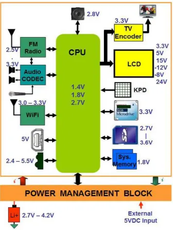
Fig. 1.1 shows typical power supply rails used in the common portable
battery-powered electronic devices. As shown in this figure, the battery voltage change from
4.2V to 2.7V and each components in the system needs the fixed or variable voltage
irrespective of the battery voltage. In order for the system to have stable operation with
wide voltage variation, the wide range DC-DC converter is necessary.
Currently, most controller of the wide range converter is compensated by external
Source : http://www.freescale.com/files/training_pdf/VFTF09_AC109.pdf
network is designed by the end users according to the worst case condition. This
conven-tional design may lose the performance at other operating conditions and need the end
users to discover the suitable compensation network to make the converter work stable.
However, if the controller can make the power plant transfer functions as constant as
possible for all operating points, the aforementioned issues are solved. That is that a
fixed compensator can make the converter operate stable with higher performance and
that the fixed compensator can be integrated into the controller for the end users not to
think of designing a proper compensator.
It is well known that the line regulation of the current programmed mode control is
superior to that of voltage mode control. It also has been reported that the conventional
current programmed mode control shows the smooth transition between CCM
(Contin-uous Conduction Mode) and DCM (Discontin(Contin-uous Conduction Mode) [22]. It is shown
in [22] that when using current-mode control, there is little change in either the stability
margin or the closed-loop performance when crossing the boundary between continuous
and discontinuous mode of operation. These characteristics shows that the conventional
current programmed mode control is suitable to the wide voltage range converter.
Power density and response speed are important performance metrics in DC-DC
power converters for mobile applications [23]. Both of these metrics can be improved
by increasing the switching frequency of the converters. The higher switching
frequen-cies are allowed to use the small valued passive components which make the physical size
of the converters. These smaller passive components provide faster response to change
in operating conditions with the help of a shorter switching period. This faster response
is very crucial on some applications such as envelope modulator for polar modulation
applications. Therefore, there has been strong motivation to move to increased switching
This dissertation proposes a new double edge current mode control (DECPM) for
wide range and high frequency application. Detail analysis on the proposed DECPM will
be addressed and the physical implementation of the DECPM into the high frequency
10MHz 4 switch buck boost converter will be shown. Therefore, DECPM will be verified
to overcome the aforementioned issues such as stable operation with wide voltage range
and high frequency operation.
1.2
Dissertation Outline
In chapter 2, the conventional current programmed mode control (CPM) is reviewed.
The steady state condition and the subharmonic issues are derived again. The
sample-data model of the peak CPM is revisited and its small signal model is shown by deriving
the modulation gain (Fm) and sampling gain (He). The Ridley’s method is used for this
modeling.
Chapter 3 introduces the double edge current program mode control (DECPM) and
its modeling. This chapter starts from the derivation the steady state conditions and
the subharmonic oscillation issues. A sample-data model for DECPM is proposed by
mathematically combining the conventional peak CPM and valley CPM models. The
de-pendence of the sampling frequency on the duty ratio is analyzed through this modeling.
A small signal model for DECPM is developed by deriving the modulation gains (Fm) and
sampling gains (He). The proposed DECPM model is compared with the conventional
single CPM by SIMPLIS simulations. The larger current loop gain at high frequency
for DECPM than single CPM will be verified. This large current loop gain introduces
DECPM to the high frequency and wide range DC-DC converter applications, and this is
buck boost converter (4SBBC) in chapter 4.
Chapter 4 shows the architecture of the 4SBBC which is made of JAZZ 0.5µm. This
chapter also show the detail design of the key blocks for the 4SBBCS such as current
sensor and ramp signal generator. The measurement results show that the implemented
4SBBC with DECPM works well with a switching frequency of 10MHz and with with
wide range input and output voltage.
Chapter 5 show the power stage optimization of the 4SBBC for polar modulation
application. Differ from the conventional DC-DC applications, the output voltage of the
4SBBC changes dynamically for the polar modulation. This chapter briefly introduces
the polar modulation application for the DC-DC converter and the characteristics of the
EDGE signal which is used as a reference signal to the 4SBBC. This chapter shows the
detail power loss break-downs of the 4SBBC and its power stage optimization based on
average energy efficiency for the EGDE signal.
Chapter 2
Review of the conventional Current
Programmed Mode Control (CPM)
2.1
Introduction : Current Programmed Mode
Con-trol
Current Programmed Mode control (CPM) is widely accepted and used in industry due
to its inherent over-current protection, superior dynamic response, and ease of
implemen-tation of current sharing [22, 24, 25, 26, 27, 28, 29, 30, 31, 32, 33]. Current Programmed
Mode control (CPM) is also called as current mode control. CPM can be divided into
peak CPM and valley CPM depending on the modulation scheme. As expected from the
naming, the peak CPM modulates the PWM signal by limiting the peak value of the
sensed inductor current signal and the valley CPM does it by limiting the valley value of
the sensed inductor current signal.
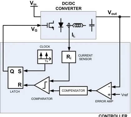
-+
COMPARATOR
Vref
COMPENSATOR
CONTROLLER
ERROR AMP
V
inV
outR
iS
R
Q
Ts CLOCK
CURRENT SENSOR
DC/DC
CONVERTER
I
LV
GLATCH
CPM. Different from voltage mode control, CPM does not have saw tooth signal to
modulate the PWM duty signal. Instead of the saw tooth signal, CPM uses the inductor
current signal to modulate the PWM duty signal. In the Peak CPM, the power switch
is turned off when the sensed inductor current is larger than control signal (vc) which is
the output of compensator in Fig. 2.1 [34][24]. As a result, the peak point of the sensed
inductor current is controlled and this modulates the PWM duty signal.
Because of the well known subharmonic oscillation problem when duty cycle is larger
than 0.5 in peak CPM [34], the conventional CPM needs a ramp signal added in the
control loop. Fig.2.2 is a modified peak CPM block diagram with an additional ramp
generator. In the steady state, the peak point of the sensed inductor current is limited
by the control signal (vc) and the ramp signal which is shown in Fig.2.3.
This chapter will revisit the conventional peak CPM. The steady state conditions
are shown, and the subharmonic oscillation issue and its solution will be revised first.
The sample-data modeling of the peak CPM will be shown here again. The step-by-step
derivations of the sample-data modeling of the peak CPM is revisited and the bandwidth
limitation due to the sample-hold effect at the switching frequency is shown.
2.2
Steady State condition and Subharmonic
Oscil-lation
In this section, the steady state condition and subharmonic oscillation problem of the
peak CPM are revisited.
Fig.2.3 shows the steady state waveforms of the sensed inductor current (Ri ·iL),
COMPARATOR
Vref
COMPENSATOR
CONTROLLER
ERROR AMPV
inV
outR
iS
R
Q
Ts CLOCK
CURRENT SENSOR
DC/DC
CONVERTER
I
LV
GLATCH
-+
+
+
Ma ARTIFICIAL
RAMP
ANALOG ADDER
m1 -ma
-m2
Ts
D Ri·iL
vc
Ri·ip
t D
0 Ts
Figure 2.3: Steady state waveform of the sensed inductor current in Peak CPM with ramp signal
value of the sensed inductor current. From the Fig.2.3, the peak (Ri ·ip) of the sensed
inductor current are derived in terms of the control signal (vc), the rising slope of the
sensed inductor current (M1) and duty (D).
Ri·ip =Ri·iL(DTs) =vc−maDTs =Ri·iL(0) +m1DTs (2.1)
To see the steady state condition of the sensed inductor current (Ri·iL), the
relation-ship of the sensed inductor currents between the adjacent switching periods are derived
as shown below.
Ri ·iL(Ts) = Ri·ip −m2D′Ts
= Ri·iL(0) +m1DTs−m2D′Ts (2.2)
m1 -ma
-m2
Ts
D
Ri·iL
vc
Ri·ip
t D
ˆ (0)
i L R i⋅⋅⋅⋅
ˆ ( ) i L s
R i T⋅⋅⋅⋅
Steady-state Waveform
Perturbed Waveform ˆ (2 )
i L s
R i⋅⋅⋅⋅ T
s T dˆ
Figure 2.4: Steady-state and perturbed sensed inductor current waveforms in peak CPM
steady state condition of peak CPM is derived from (2.2), and is
m2
m1
= D
D′ (2.3)
For analyzing the subharmonic oscillation issues [34] in peak CPM, the sensed
in-ductor current is perturbed as shown in Fig. 2.4. Then, the subharmonic oscillation
conditions can be derived from the natural response of the sensed inductor current
per-turbation (Ri·iˆL).
From the simple trigonometric analysis of Fig. 2.4, the following equations are derived.
Ri·iˆL(0) =madTˆ s+m1dTˆ s = (m1 +ma) ˆdTs (2.4)
Ri·iˆL(Ts) =madTˆ s−m2dTˆ s=−(m2−ma) ˆdTs (2.5)
From the above two equations, the following is derived directly.
ˆ
iL(Ts) =−
m2−ma
m1+ma
ˆ
By generalizing (2.6) with arbitrary timing, and it is
ˆ
iL(nTs) = −
m2−ma
m1+ma
·iˆL((n−1)Ts)
ˆ
iL(nTs) = αp·iˆL((n−1)Ts) (2.7)
αp = −
m2−ma
m1+ma
, 1−αp =
m1+m2
m1+ma
(2.8)
(2.7) is a inductor current perturbation relationship between the adjacent switching
periods in peak CPM. Here, αp is the inductor current attenuation factor for the peak
CPM. By using the steady state condition of peak CPM in (2.3), αp in (2.8) is rewritten
in terms of the duty ratio, the slope of ramp signal and the falling slope of the sensed
inductor current as shown below.
αp =
1− ma
m2
D′ D +
ma
m2
(2.9)
By doing similar derivation, the inductor current attenuation factor for the valley
CPM (αv) is derived like following.
αv = −
m1−ma
m2+ma
(2.10)
=
D′ D −
ma
m2
1 + ma
m2
(2.11)
It is well known that, without the ramp signals (Ma = 0),αp for peak CPM and αn
for valley CPM become larger than 1 when D > 0.5 and D < 0.5 respectively, which
causes subharmonic oscillation. The inductor current attenuation factors of the peak and
0 0 .5 1 0
1 0 2 0 3 0
0 0 .5 1
0 1 0 2 0 3 0
Duty Cycle
p
Duty Cycle
v
Figure 2.5: αp and αv at the function of duty cycle without artificial ramp
2.5.
αp|M
a=0 =
D
D′ (2.12)
αv|Ma=0 = D
′
D (2.13)
To avoid subharmonic oscillations for the entire duty range, the inductor current
attenuation factors should be less than 1 for all operating conditions (i.e. for all duty
ratios). This is done by adding the ramp signal with an appropriate slope (ma). One
common choice of thema in peak CPM not to have subharmonic oscillation for all duty
range is
ma=
1
With this choice of the ma, |αp| <1 for 0≤ D < 1 and αp =−1 at D= 1. This is the
minimum value of ma which make the system stable for all duty cycles. [34]
2.3
Sample-data modeling
There has been much research on control modelings for high frequency converters which
can predict up to half the switching frequency [35, 36, 37, 24, 32, 31, 25]. In order to model
the current programmed mode control accurately to high frequency including the sample
and hold effects, the sample-data model is popular and widely accepted [24, 32, 31].
During this section, the sample-data modeling technique of the Ridley’s method [24]
to derive the current feedback transfer function of the peak CPM is reviewed. After
this derivation, a popular small signal model of the peak CPM is used to derive the
modulation gain (Fm) and sampling gain (He) by comparing with the derived the
sample-data current feedback transfer function, which can apply to design the compensator for
t t s T (Exact) (approx) t s T D) 1 ( −−−− ˆ [ ]c
v n s DT ) (t D ˆ [ ] i L
R i n⋅⋅⋅⋅
ˆ [ ]
i L
R i n⋅⋅⋅⋅
ˆ [ 1]
i L
R i n⋅⋅⋅⋅ −−−−
ˆ [ 1]
i L
R i n⋅⋅⋅⋅ ++++
s
T n
dˆ[ ] dˆ[n++++1]Ts
C
v
ˆ
C C v ++++v
i L
R i⋅⋅⋅⋅
ˆ
( )
i L L
R ⋅⋅⋅⋅ i ++++i
-m
am
1-m
2-m
a ˆ ( ) i LR i t⋅⋅⋅⋅
ˆ ( )
i L R i t⋅⋅⋅⋅
ˆ [ 1]
i L
R i n⋅⋅⋅⋅ −−−− ˆ [ ]
i L
R i n⋅⋅⋅⋅ ˆ [ 1]
i L
R i n⋅⋅⋅⋅ ++++
2.3.1
Sample-data current feedback transfer function
Fig. 2.6 shows the waveforms to derive the sample-data model for the peak CPM. This
figure shows the modulated duty signal ( ˆd) and the sensed inductor current perturbation
(Ri·iˆL) as the results of the control signal perturbation ( ˆvc). As shown in Fig. 2.6, it can
be observed that the sensed inductor current (Ri ·iˆL) is updated once in one switching
period (Ts). The inductor current perturbation happens only once in each switching
period and is held for one switching period [24]. This makes the sampling frequency
of the control the same as the switching frequency of the power stage. Therefore, the
conventional CPM (here, peak CPM) has a fixed switching frequency in the power stage
and a fixed sampling frequency for the control. For this reason, the switching frequency
and the sampling frequency of the conventional CPM is considered as a same.
For the following peak CPM modeling, the voltages applied across the inductor are
kept constant and the current feedback loop is closed [24]. By using simple trigonometric
analysis at the time of (n−D)Ts from Fig. 2.6, the following two equations are derived.
Ri ·iˆL[n] = Ri·iˆL[n−1] + (m1+m2) ˆd[n]Ts (2.15)
ˆ
vc[n] = Ri·iˆL[n−1] + (m1+ma) ˆd[n]Ts (2.16)
By eliminating ˆd[n]Ts and combining (2.15) and (2.16), the following equation is derived.
Ri·iˆL[n] =−
m2−ma
m1+ma
Ri·iˆL[n−1] +
m1+m2
m1+ma
ˆ
vic[n] (2.17)
(2.17) can be rewritten and it is
Ri·iˆL[n] =αp ·Ri·iˆL[n−1] + (1−αp)·vˆc[n] (2.18)
This (2.18) is the well known discrete time inductor current dynamics of the peak CPM
which shows the relation of the sensed inductor current perturbation (Ri ·iˆL) and the
control signal perturbation ˆvc) during one switching period of Ts [32].
By applying the Z-transform equivalent to (2.18), the discrete time current feedback
transfer function of the peak CPM in Z-domain is derived and it is
Ri·iˆL[n]
ˆ
vc[n]
= 1−αp
1−αpz−1
(2.19)
In order to change it from the discrete time transfer function to a continuous time transfer
function,z =e−sTs and zero order hold function(ZOH) which hold the sampled value for
Ts are applied to (2.19). Then, the sampled-Laplace domain current feedback transfer
function of the peak CPM with ZOH for one switching period of Ts [24, 32] is
Ri·iˆL(s)
ˆ
vc(s)
= 1−αp
1−αpe−sTs
· 1−e −sTs
sTs
(2.20)
2.4
Small Signal Model for CPM
In order to design feedback circuit and apply it to DC-DC converter, it is necessary to
develop a small signal model of current programmed mode control scheme with average
power stage model. Fig.2.7 shows the well known current mode control small signal
model diagram with averaged power stage model [34].
G
id(s)G
vg(s)G
ig(s)+ +
+ +
G
vd(s)F
v_ +_
F
gF
mH
e(s)R
i(s)o
v
ˆ
L
i
ˆ
g
v
ˆ
L
i i
R ⋅⋅⋅⋅ˆ
d
ˆ
+_ˆ
c
v
m1 -m2
ma
Sensed inductor current (Ri · iL)
Artificial ramp signal
Comparator
Duty Cycle (d)
Control signal (vc)
Figure 2.8: Modulation in peak CPM
2.7 [34]. Gvd is the duty to output voltage transfer function, Gid is the duty to inductor
current transfer function,Gvg is the input voltage to output voltage transfer function and
Gig is the input voltage to inductor current transfer function. These transfer functions
are from the well known average power stage model [34]. Peak CPM related blocks are
Fm, He, Fv and Fg which are the modulation gain, the sampling gains, the feedforward
gain from output voltage and the feedforward gain from input voltage respectively. And
Ri represents the inductor current sensing gain.
In this section, the CPM related control blocks (gains) are revisited and the associated
gains of peak CPM are derived. For valley CPM, readers can follow the method shown
here to derive the equations.
2.4.1
Modulation gain (
F
m) derivation
The Fm is known as a modulation gain. In peak CPM, the duty cycle is generated from
the comparator with the control signal, the sensed inductor current, and the ramp signal.
signal approximation, Fm can be derived like below.
Fm =
1 (m1+ma)Ts
(2.21)
This Fm also can be derived from the the small signal model of [24]. From the small
signal model, the modulation gain (Fm) can be defined as the ratio of the ‘current’ duty
perturbation ( ˆd[n]) to the difference of the ‘current’ control signal perturbation ( ˆvc[n])
and the ‘previous’ sensed inductor current perturbation (Ri·iˆL[n−1]), and it is
Fm ≡
ˆ
d[n] ˆ
vc[n]−Ri·iˆL[n−1]
(2.22)
By assuming Fv = 0, Fg = 0, and He = 1 in Fig.2.7, the Fm is derived from the (2.16)
like below ans shows same as (2.21).
Fm =
ˆ
d
ˆ
vc −Ri·iˆL
= 1
(m1+ma)Ts
(2.23)
2.4.2
Sampling gain (
H
e) derivation
The He is a sampling gain to model the sample-hold effect which is derived from the
sample-data modeling shown in previous chapter. This gain has been derived with
dif-ferent ways from difdif-ferent authors so far. In this paper, Dr. Ridley’s method is used to
derive the He [24].
From the Fig.2.7, the response of ˆiL to ˆvc can be written like below.
ˆ
iL(s)
ˆ
vc(s)
= FmGid
1 +FmGidRiHe
And, by rewriting (2.20), the following equation is derived.
ˆ
iL(s)
ˆ
vc(s)
= 1
Ri
1−αp
1−αpe−sTs
· 1−e −sTs
sTs
(2.25)
Because (2.24) and (2.25) are same, theHe can be derived by equating (2.24) and (2.25)
like below.
FmGid
1 +FmGidRiHe
= 1
Ri
1−αp
1−αpe−sTs
1−e−sTs
sTs
(2.26)
At first, Gid which is independent to power stage topologies need to be derived. Gid is
the gain from duty perturbation ( ˆd) to inductor current perturbation ( ˆiL) as shown in
Eq.(2.27)
Gid ≡
ˆ
iL
ˆ
d (2.27)
Fig.2.9 is the small signal model of the power stage and CPM model with fixed voltages
[24][38]. From Fig.2.9, the Gid can be derived and expressed for all converters as follow.
Gid(s) =
Vap
s·L Vap = Vac+Vcp
m1 =
Ri·Vac
L , m2 =
Ri·Vcp
L Gid(s) =
1
Ri
m1+m2
s (2.28)
With this (2.28), (2.23) can be rewritten like below.
Fm·Gid=
1
Ri
1−αp
s·Ts
F
mH
e(s)R
i(s)ˆ
c
v
d
I
Lˆ
+_
L
d
D
V
apˆ
L
i
ˆ
p a
c PWM
1
D
d
ˆ
With (2.29) and (2.26), the following is derived,
1 +Fm·Gid·Ri·He =
esTs−α
p
esTs −1 (2.30)
From the above, the sampling gain (He) is derived and it is
He=
sTs
esTs −1 (2.31)
In [24], the (2.31) is approximated like below.
He(s) ∼= 1 +
s ωnQz
+ s
2
ω2
n
(2.32)
where,
Qz = −2
π
and,
ωn =
π Ts
This (2.32) is the second order model of (2.31) and shows that the sampling gain (He)
has the complex double zeros at the half the switching frequency (fs = 1/Ts). From the
(2.24), it can be expected that the double zeros of the He will bring the double poles of
the system. For this reason, it is well known that this double zeros of the He at the half
the switching frequency limit the system performance which use the conventional CPM
Chapter 3
Double Edge Current Programmed
Mode Control
3.1
Introduction: background and previous works
on double edge modulation
In the previous chapter 2, we revisited Current Programmed Mode control (CPM). From
the duty modulation point of view, the conventional CPM which is either the peak CPM
or valley CPM is a single edge modulation scheme. The peak CPM only can modulate
the trailing edge of the duty, and valley CPM only can modulate the leading edge of the
duty during one switching period.
Fig.3.1 and Fig.3.2 shows the conceptual duty modulation examples for the peak CPM
and valley CPM respectively. As shown Fig.3.1 and Fig.3.2, in conventional single edge
current programmed mode control (hereafter referred to as “single CPM”), only one edge
T
sDuty
cycle
Figure 3.1: Trailing edge modulation
T
sDuty
cycle
Figure 3.2: Leading edge modulation
T
sDuty
cycle
Figure 3.4: Sampling scheme of the PWM comparator:(a) trailing-edge PWM, and (b) double-edge PWM.
is unmodulated and determined by a fixed clock. In other words, the inductor current
information is updated only once during a single switching period (Ts). Therefore, the
bandwidth of a system utilizing single CPM is limited to half the switching frequency
due to the corresponding sample and hold effects [24, 25, 31, 32, 39, 40].
Other authors have investigated double edge modulation schemes for converter
ap-plications. [41] addresses double edge modulation for voltage mode control and shows
that the sampling frequency is doubled when the duty ratio is 0.5. Fig. 3.4 is the
sam-pling scheme difference between trailing-edge PWM and the double-edge PWM in voltage
mode control shown in [41]. In this reference, the author comments that “Intuitively, the
double-edge PWM has a sampling frequency twice that of the trailing-edge PWM.” and
shows that the dip on the transfer function ofGvc at two times of the switching frequency
Figure 3.5: Gvc with double edge-PWM in SIMPLIS simulation: (a) duty cycle is 50%,
Figure 3.6: The schematics of the pulse width modulators.
[42] and [43] investigated the potential of a double (dual) edge controller for VRM
applications to achieve the fast transient response. These papers emphasize the small
switching delay in the control loop due to the double edge modulation scheme. [42]
claims that dual edge controller reduces the switching action delay. Fig. 3.7 is the
conceptual waveforms of the switching delays with different types of the pulse width
modulators which is shown in Fig. 3.6 in [42]. The author explains that “The trailing
edge modulator has a delay (td) when the load steps up and the leading edge modulation
has delay when the load releases. This switching action delay causes undesirable charging
or discharging of the output capacitors and results in the output voltage peaks or dips.
In order to eliminate this delay, the dual edge modulator without RS latch is used. The
dual edge controller should be well designed in IC level to be immune to the switching
noise.”
[44] comments that a double edge control scheme can improve the tracking accuracy
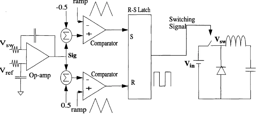
of the output voltage to the reference signal. Fig. 3.8 is the schematic which is proposed
in [44]. One comparison between the feedback signal (Sig) and a ramp is used to set the
Figure 3.8: Two sided latched PWM shematics
to reset the switch. There is an extra comparator compared to a conventional PWM
controller.
However, the sampling frequency dependence on the duty ratio and other
characteris-tics of DECPM, such as the subharmonic oscillation issue and a larger current loop gain
than conventional CPM, have not been analytically investigated from above research.
This dissertation will address the detailed analysis of DECPM with a newly proposed
model.
In this chapter, sample-data modeling of the double edge current programmed mode
control (DECPM) is newly proposed and analyzed. The steady state conditions and
the subharmonic oscillation issue of DECPM are analyzed first. Sample-data modeling
for DECPM is proposed by mathematically combining the conventional peak CPM and
valley CPM models. The dependence of the sampling frequency on the duty ratio is
-Ma
-M2
Ts
H=2Ma×Ts
Ri·iL vc
vc-H
Ri·ip
Ri·iv
t 0
M1
Ma Ramp signals
s
T
D1 D1′′′′Ts D2′′′′Ts D2Ts 0.5Ts
Figure 3.9: Steady state inductor current waveform in DECPM
deriving the modulation gains (Fm) and sampling gains (He). The proposed DECPM
model is compared with the conventional single CPM by the SIMPLIS simulations. The
larger current loop gain at high frequency for DECPM than the single CPM will be
verified in this section.
3.2
Steady State condition and Subharmonic
Oscil-lation
In this section, the steady state and subharmonic oscillation conditions of DECPM are
discussed. Fig. 3.9 shows the steady state waveforms of the sensed inductor current
(Ri ·iL), control signal (vc) and ramp signals in DECPM. Here, Ri is the gain of the
current sensor. In DECPM, two ramp signals with the slopes of Ma and−Ma are added
to the control signal (vc) to control the peak and valley value of the sensed inductor
current. As shown in Fig. 3.9, because both peak and valley values of the sensed
inductor current are controlled by DECPM, the resultant duty signals are modulated on
From Fig. 3.9, the peak (Ri ·ip) and valley value (Ri ·iv) of the sensed inductor
current are derived in terms of the control signal (vc).
Ri ·ip = Ri·iL(D1Ts)
= vc−MaD1Ts =Ri·iL(0) +M1D1Ts (3.1)
Ri·iv = Ri·iL((0.5 +D2′)Ts)
= Ri·iL(D1Ts)−M2·(D′1+D′2)·Ts (3.2)
Here, D1 andD2 are the duty ratios in the peak and valley current control region
respec-tively. Therefore, D′
1 = 0.5−D1 and D2′ = 0.5−D2, and the whole duty ratio (D) is a
sum of these D1 and D2.
To see the steady state condition of the sensed inductor current (Ri·iL), the
relation-ship of the sensed inductor currents between the adjacent switching periods are derived
as shown below.
Ri·iL(Ts) = Ri·iv+M1D2Ts
= Ri·iL(0) +M1D1Ts−M2·(D1′ +D′2)·Ts+M1D2Ts
= Ri·iL(0) +M1·(D1+D2)·Ts−M2·(D1′ +D2′)·Ts
= Ri·iL(0) +M1DTs−M2D′Ts (3.3)
In steady state, the condition of Ri ·iL(Ts) = Ri ·iL(0) should be satisfied. Thus, the
steady state condition of DECPM is derived from (3.3), and is
M2
M1
= D
-
M
2 ) 0 ( ˆ L i i R ⋅⋅⋅⋅ ) 2 ( ˆ s L i T i R ⋅⋅⋅⋅)
(
ˆ
s L ii
T
R
⋅⋅⋅⋅
s
T
d
ˆ
2 sT
d
ˆ
1−−−−
2
s
T
T
s0
M
1v
cv
c-H
s
T
D
1 sT
d
D
ˆ
)
(
1−−−−
1s s
T
D
T
22
++++
′′′′
ss
T
d
D
T
)
ˆ
(
2
++++
2′′′′
++++
2M
a-M
at
Steady-state Waveform Perturbed Waveform sT
D
1D
1′′′′
T
sD
2′′′′
T
sD
2T
sFigure 3.10: Steady-state and perturbed inductor current waveforms
This steady state condition of DECPM is same as that of the conventional single CPM.
For analyzing the subharmonic oscillation issues [34] in DECPM, the sensed inductor
current is perturbed as shown in Fig. 3.10. Then, the subharmonic oscillation conditions
can be derived from the natural response of the sensed inductor current perturbation
(Ri·iˆL).
From simple trigonometric analysis of Fig. 3.10, the following equations are derived.
Ri·iˆL(0) = −(M1+Ma) ˆd1Ts (3.5)
Ri·iˆL(
Ts
2 ) = −(Ma−M2) ˆd1Ts (3.6)
Ri·iˆL(
Ts
2 ) = (Ma+M2) ˆd2Ts (3.7)
Because (3.6) and (3.7) are equal,
ˆ
d2 =
−(Ma−M2)
Ma+M2
·dˆ1 (3.9)
By plugging (3.9) into (3.8) and generalizing it to arbitrary timing,
Ri·iˆL(nTs) =−
M2−Ma
M1+Ma
· −M1−Ma
M2+Ma
·Ri ·iˆL((n−1)Ts) (3.10)
ˆ
iL(nTs) =αp·αv·iˆL((n−1)Ts) (3.11)
=α·iˆL((n−1)Ts) (3.12)
where,
α =αp·αv (3.13)
αp =−
M2−Ma
M1+Ma
, 1−αp =
M1 +M2
M1+Ma
(3.14)
αv =−
M1−Ma
M2+Ma
, 1−αv =
M1+M2
M2 +Ma
(3.15)
(3.12) is a inductor current perturbation relationship between the adjacent switching
periods. Here,αp and αv are the inductor current attenuation factors for the peak CPM
and valley CPM respectively, and α is the inductor current attenuation factor for the
DECPM which is a product of αp and αv as shown in (3.13). By using the steady state
condition of DECPM in (3.4), α in (3.13) is rewritten in terms of the duty ratio, the
slope of ramp signal and the falling slope of the sensed inductor current as shown below.
α=αp·αv =
1− Ma
M2 D′ D + Ma M2 · D′ D − Ma M2
1 + Ma
M2
(3.16)
It is well known that, without the ramp signals (Ma = 0), αp for peak CPM and αn
Duty Cycle
0 0.5 1
1 2 3 4 5
|α
p|
|α
v|
α=|α
p·α
v|
Figure 3.11: α,αp and αv at the function of duty ratio without ramp signal (Ma = 0)
causes subharmonic oscillation. The inductor current attenuation factors without the
ramp signals (Ma = 0) are derived below and showed in Fig. 3.11.
αp|Ma=0 = D
D′ (3.17)
αv|Ma=0 = D
′
D (3.18)
α|Ma=0 = 1 (3.19)
Interestingly, the α in DECPM, which is a product of αp and αn is always 1 for the
entire duty range without the ramp signals (Ma = 0). This means once perturbation is
applied to inductor current, there is no amplification or attenuation of the disturbance
in DECPM.
To avoid subharmonic oscillations for the entire duty range, the inductor current
attenuation factors should be less than 1 for all operating conditions (i.e. for all duty
K=0.01
K=0.1
K=0.5
K=1
K=2
K=10
K=100
0
0.2
1
Duty Cycle
0.4
0.6
0.8
0.2
0.4
0.6
0.8
1
0
α
Figure 3.12: αat the function of duty ratio with different ramp signals having the slopes
terms of the duty ratios. Here, K is the ratio of the slopes of the ramp signal and the
falling slope of the sensed inductor current (K = Ma/M2). Fig. 3.12 shows that α will
always be less than 1 for the whole duty range, regardless of the slope of the ramp signal
in DECPM. However, for conventional single CPM, the slope of the ramp signals (Ma)
need to be chosen carefully to avoid subharmonic oscillation for all duty ranges [34].
3.3
Sample-data modeling
3.3.1
Sample-data current feedback transfer function
There has been much research on control modelings for high frequency converters which
can predict up to half the switching frequency[35, 36, 37, 24, 32, 31, 25]. In order to
model the current programmed mode control accurately to high frequency including the
sample and hold effects, the sample-data model is popular and widely accepted[24, 32, 31].
Among the sample-data modelings for converters, Ridley’s method[24, 25] is referred and
applied to model the DECPM in this dissertation.
Fig. 3.13 shows the waveforms to derive the sample-data model for DECPM. This
figure shows the modulated duty signal ( ˆd) and the sensed inductor current perturbation
(Ri·iˆL) as the results of the control signal perturbation ( ˆvc). As shown in Fig. 3.13, it can
be observed that the sensed inductor current (Ri·iˆL) is updated twice in one switching
period (Ts). This is a major difference between DECPM and conventional single CPM.
In conventional single CPM, the inductor current perturbation happens only once in
each switching period and is held for one switching period [24]. This makes the sampling
frequency of the control the same as the switching frequency of the power stage. However,
one switching period, and each updated inductor current perturbation is kept (held) for
DTs and (1−D)Ts respectively. Therefore, DECPM has a fixed switching frequency in
the power stage but variable sampling frequency for the control with different operating
C
v
s
T
n
d
ˆ
[
]
−−−−
)] 1 ( [
ˆ n D
i
Ri⋅⋅⋅⋅ L −−−− −−−−
s T ) ( ˆ t i Ri ⋅⋅⋅⋅ L
(Exact)
(approx) Ri⋅⋅⋅⋅iˆL[n]
]
[
ˆ
n
v
c ] 1 [ ˆ −−−−⋅⋅⋅⋅i n
Ri L
s T D) 1 ( −−−− )] 1 ( [
ˆ n D
vc −−−− −−−−
s
T D n
dˆ[ −−−−(1−−−− )]
s
DT
] [
ˆ n D
i Ri⋅⋅⋅⋅ L ++++
) (t D
-
M
aM
aM
1-M
2 ] 1 [ ˆ −−−−⋅⋅⋅⋅i n
Ri L
] [ ˆ n
i Ri⋅⋅⋅⋅ L
] [
ˆ n D
i Ri⋅⋅⋅⋅ L ++++
t
t
t
]
[
ˆ
n
i
R
i⋅⋅⋅⋅
L)] 1 ( [
ˆ n D
i
Ri⋅⋅⋅⋅ L −−−− −−−−
)] 1 ( [
ˆ n D
i
Ri⋅⋅⋅⋅ L −−−− −−−−
s T 5 . 0 ) ( ˆ t i Ri⋅⋅⋅⋅ L
H
v
C−−−−
C
C
v
v
++++
ˆ
H
v
v
C++++
ˆ
C−−−−
] [
ˆ n D
i Ri ⋅⋅⋅⋅ L ++++
] 1 [ ˆ −−−−
⋅⋅⋅⋅i n
Ri L
((((
n−−−−(1−−−−D)))))
Ts nTs((((
n++++D))))
TsFor the following DECPM modeling, the voltages applied across the inductor are kept
constant and the current feedback loop is closed as in conventional CPM modeling [24].
In addition, it is also assumed that the control signal perturbation ( ˆvc) does not change
during one switching cycle (Ts). This assumption implies that, for one switching period,
the first updated inductor current perturbation does not affect the control signal
pertur-bation ( ˆvc) which is also used for the second update of the inductor current perturbation.
Therefore, the first update and the second update of the inductor current perturbations
are independent from each other with respect to the control signal perturbation ( ˆvc).
By using simple trigonometric analysis at the time of (n−(1−D))Tsfrom Fig. 3.13,
the following two equations are derived.
Ri ·iˆL[n−(1−D)] =Ri·iˆL[n−1] + (M1+M2) ˆd[n−(1−D)]Ts (3.20)
ˆ
vc[n−(1−D)] =Ri·iˆL[n−1] + (M1+Ma) ˆd[n−(1−D)]Ts (3.21)
These (3.20) and (3.21) show the relationship among the control signal perturbation
( ˆvc), the peak point of the sensed inductor current perturbation (Ri·iˆL) and the duty
perturbation ( ˆd). This relationship is called a ‘peak current control law’ in this
disserta-tion.
With a similar derivation at the time of nTs from Fig. 3.13, the other two
equa-tions are derived in (3.22) and (3.23). These two equaequa-tions show the relaequa-tionship
be-tween the control signal perturbation ( ˆvc), the valley point of the sensed inductor current
perturbation(Ri·iˆL) and the duty perturbation ( ˆd). This relationship is called a ‘valley
Ri·iˆL[n] =Ri·iˆL[n−(1−D)] + (M1+M2)(−dˆ[n])Ts (3.22)
ˆ
vc[n] =Ri·iˆL[n−(1−D)] + (M2+Ma)(−dˆ[n])Ts (3.23)
In conventional single CPM, either one set of (3.20),(3.21) or (3.22),(3.23) is used for
peak CPM and valley CPM respectively, but DECPM needs both of them.
With (3.20) and (3.21), a following equation is derived.
Ri·iˆL[n−(1−D)] =αp ·Ri·iˆL[n−1] + (1−αp)·vˆc[n−(1−D)] (3.24)
By applying a Laplace transform, it’s time shift property and hold function for (1−D)Ts
to (3.24), the ‘peak current control law’ based current feedback transfer function of
DECPM is derived in (3.25), which looks similar to that of peak CPM.
Ri·iˆL(s)
ˆ
vc(s)
peak
= 1−αp
1−αpe−sDTs
· 1−e
−s(1−D)Ts
sTs
(3.25)
The difference between (3.25) and the conventional sampled data current feedback
trans-fer function of peak CPM[24] is the duty information in the model. The DTs in the first
term of the right hand side of (3.25) means the derived transfer function is the result
of the relationship between the control signal perturbation ( ˆvc) and the sensed inductor
held for (1−D)Ts. Therefore, the duty information in the transfer function of DECPM
shows that the sampling frequency of the control (not the switching frequency of the
power stage) varies with the different operating points.
By doing a similar derivation with (3.22) and (3.23), the ‘valley current control law’
based current feedback transfer function of DECPM is derived in (3.26).
Ri ·iˆL(s)
ˆ
vc(s)
valley
= 1−αv
1−αve−s(1−D)Ts
· 1−e −sDTs
sTs
(3.26)
Similar to (3.25), the (1−D)Ts in the first term of the right hand side of (3.26)
indicates that the derived transfer function is the result of the relationship between the
control signal perturbation ( ˆvc) and the sensed inductor current perturbation (Ri ·iˆL)
during (1−D)Ts, and the DTs in the second term implies that the sampled (updated)
information of the sensed inductor current perturbation is held for DTs.
The whole current feedback transfer function of DECPM during one switching period
is a linear sum of the (3.25) and (3.26) and is shown in (3.27). This is deduced from
the time domain waveform of Ri · iˆL(t) (approx) shown at the last waveform in Fig.
3.13. The value of Ri ·iˆL[n] is a sum of the two updated values from DECPM and the
value of Ri ·iˆL[n−1]. These two updated values in time domain correspond to (3.25)
and (3.26) in frequency domain. In other words, with the assumption of the constant
control signal perturbation ( ˆvc) during one switching period as mentioned earlier, the
two updates of the sensed inductor current perturbation in DECPM are independent
each other. Therefore, the corresponding transfer functions of (3.25) and (3.26) are also
104 105 106 107 -40 -20 0 frequency [Hz] m a g n it u d e [ d B ]
(Ri*iL)/vc magnitude and phase responses
DECPM Peak CPM Valley CPM
104 105 106 107
-180 -135 -90 -45 0 45 frequency [Hz] p h a s e [ d e g ]
Figure 3.14: vc to Ri·iL responses when Vin = 3.3V and Vout= 0.1V
feedback transfer function of DECPM during one switching period the linear sum of the
(3.25) and (3.26).
Ri·iˆL(s)
ˆ
vc(s)
= Ri·iˆL(s) ˆ
vc(s)
peak
+ Ri·iˆL(s) ˆ
vc(s)
valley
= 1−αp
1−αpe−sDTs
· 1−e
−s(1−D)Ts
sTs
+ 1−αv
1−αve−s(1−D)Ts
· 1−e −sDTs
sTs
104 105 106 107 -40 -20 0 frequency [Hz] m a g n it u d e [ d B ]
(Ri*iL)/vc magnitude and phase responses
DECPM Peak CPM Valley CPM
104 105 106 107
-180 -135 -90 -45 0 45 frequency [Hz] p h a s e [ d e g ]
Figure 3.15: vc toRi·iL responses when Vin = 3.3V and Vout = 1.65V
104 105 106 107
-40 -20 0 frequency [Hz] m a g n it u d e [ d B ]
(Ri*iL)/vc magnitude and phase responses
DECPM Peak CPM Valley CPM
104 105 106 107
-180 -135 -90 -45 0 45 frequency [Hz] p h a s e [ d e g ]
104 105 106 107 -40 -20 0 frequency [Hz] m a g n it u d e [ d B ]
(Ri*iL)/vc magnitude and phase responses
DECPM Peak CPM Valley CPM
104 105 106 107
-180 -135 -90 -45 0 45 frequency [Hz] p h a s e [ d e g ]
Figure 3.17: vc to Ri·iL responses when Vin = 3.3V and Vout= 3.4V
104 105 106 107
-40 -20 0 frequency [Hz] m a g n it u d e [ d B ]
(Ri*iL)/vc magnitude and phase responses
DECPM Peak CPM Valley CPM
104 105 106 107
-180 -135 -90 -45 0 45 frequency [Hz] p h a s e [ d e g ]