Verifiable ASICs
Riad S. Wahby⋆◦ [email protected]
Max Howald† [email protected]
Siddharth Garg⋆ [email protected]
abhi shelat‡ [email protected]
Michael Walfish⋆ [email protected]
⋆New York University ◦Stanford University †The Cooper Union ‡The University of Virginia
Abstract—A manufacturer of custom hardware (ASICs) can under-mine the intended execution of that hardware; high-assurance ex-ecution thus requires controlling the manufacturing chain. How-ever, a trusted platform might be orders of magnitude worse in per-formance or price than an advanced, untrusted platform. This pa-per initiates exploration of an alternative: using verifiable computa-tion (VC), an untrusted ASIC computesproofsof correct execution, which are verified by a trusted processor or ASIC. In contrast to the usual VC setup, here the prover and verifiertogethermust im-pose less overhead than the alternative of executing directly on the trusted platform. We instantiate this approach by designing and implementing physically realizable, area-efficient, high throughput ASICs (for a prover and verifier), in fully synthesizable Verilog. The system, called Zebra, is based on the CMT and Allspice interactive proof protocols, and required new observations about CMT, care-ful hardware design, and attention to architectural challenges. For a class of real computations, Zebra meets or exceeds the perfor-mance of executing directly on the trusted platform.
1
Introduction
When the designer of anASIC(application specific integrated circuit, a term that refers to custom hardware) and the manufac-turer of that ASIC, known as afaborfoundry, are separate en-tities, the foundry can mount ahardware Trojan[19, 35, 105] attack by including malware inside the ASIC. Government agencies and semiconductor vendors have long regarded this threat as a core strategic concern [4, 10, 15, 18, 45, 81, 111].
The most natural response—achieving high assurance by controlling the manufacturing process—may be infeasible or impose enormous penalties in price and performance.1Right now, there are only five nations with top-end foundries [69] and only 13 foundries among them; anecdotally, only four foundries will be able to manufacture at 14 nm or beyond. In fact, many advanced nations do not have any onshore foundries. Others have foundries that are generations old; In-dia, for example, has 800nm technology [12], which is 25 years older and 108×worse (when considering the product of ASIC area and energy) than the state of the art.
Other responses to hardware Trojans [35] include post-fab detection [19, 26, 73, 77, 78, 119] (for example, testing based on input patterns [47, 120]), run-time detection and disabling (for example, power cycling [115]), and design-time obfusca-tion [46, 70, 92]. These techniques provide some assurance under certain misbehaviors or defects, but they are not sensi-tive enough to defend against a truly adversarial foundry (§10). One may also applyN-versioning [49]: use two foundries, 1Creating a top-end foundry requires both rare expertise and billions of dollars, to purchase high-precision equipment for nanometer-scale patterning and etching [52]. Furthermore, these costs worsen as thetechnology node—the manufacturing process, which is characterized by the length of the smallest transistor that can be fabricated, known as thecritical dimension—improves.
deploy the two ASICs together, and, if their outputs differ, a trusted processor can act (notify an operator, impose fail-safe behavior, etc.). This technique provides no assurance if the foundries collude—a distinct possibility, given the small number of top-end fabs. A high assurance variant is to execute the desired functionality in software or hardware on a trusted platform, treating the original ASIC as an untrusted accelerator whose outputs are checked, potentially with some lag.
This leads to our motivating question: can we get high-assurance execution at a lower price and higher performance than executing the desired functionality on a trusted platform?
To that end, this paper initiates the exploration ofverifiable ASICs(§2.1): systems in which deployed ASICs prove, each time they perform a computation, that the execution is correct, in the sense of matching the intended computation.2An ASIC in this role is called aprover; its proofs are efficiently checked by a processor or another ASIC, known as averifier, that is trusted (say, produced by a foundry in the same trust domain as the designer). The hope is that this arrangement would yield a positive response to the question above. But is the hope well-founded?
On the one hand, this arrangement roughly matches the se-tups in probabilistic proofs from complexity theory and cryp-tography: interactive proofs or IPs [22, 63, 64, 80, 102], effi-cient arguments [39, 72, 74, 83], SNARGs [62], SNARKs [36], and verifiable outsourced computation [23, 60, 63, 83] all yield proofs of correct execution that can be efficiently checked by a verifier. Moreover, there is a flourishing literature sur-rounding the refinement and implementation of these proto-cols [24, 25, 29, 31–33, 41, 51, 55, 56, 58, 59, 61, 76, 88, 98– 101, 106, 108, 112, 114] (see [117] for a survey). On the other
hand, all of this work can be interpreted as anegativeresult: despite impressive speedups, the resulting artifacts are not deployable for the application of verifiable offloading. The biggest problem is the prover’s burden: its computational over-head is at least 105×, and usually more than 107×, greater than the cost of just executing the computation [117, Fig. 5].
Nevertheless, this issue is potentially surmountable—at least in the hardware context. With CMOS technology, many costs scale down super-linearly; as examples, area and en-ergy reduce with the square and cube of critical dimension, respectively [91]. As a consequence, the performance improve-ment, when going from an ASIC manufactured in a trusted, older foundry to one manufactured in an untrusted, advanced
2This is different from, but complementary to, the vast literature on hardware
foundry, can belarger than the overhead of provers in the aforementioned systems (as with the earlier example of India). Given this gap, verifiable outsourcing protocols could yield a positive answer to our motivating question—but only if the prover can be implemented on an ASIC in the first place. And that is easier said than done. Many protocols for verifiable outsourcing [24, 25, 29, 31–33, 41, 51, 56, 58, 59, 61, 76, 88, 99–101, 114] have concrete bottlenecks (cryptographic operations, serial phases, communication patterns that lack temporal and spatial locality, etc.) that seem incompatible with an efficient, physically realizable hardware design. (We learned this the hard way; see Section 9.)
Fortunately, there is a protocol in which the prover uses no cryptographic operations, has highly structured and par-allel data flows, and demonstrates excellent spatial and tem-poral locality. This is CMT [55], an interactive proof that refines GKR [63]. Like all implemented protocols for verifi-able outsourcing, CMT works over computations expressed as
arithmetic circuits, meaning, loosely speaking, additions and multiplications. To be clear, CMT has further restrictions. As enhanced by Allspice [112], CMT works best for computations that have a parallel and numerical flavor and make sparing use of non-arithmetic operations (§2.2). But we can live with these restrictions because there are computations that have the required form (the number theoretic transform, polynomial evaluation, elliptic curve operations, pattern matching with don’t cares, etc.; see also [55, 88, 99–101, 106, 108, 112]).
Moreover, one might expect something to be sacrificed, since our setting introduces additional challenges to verifiable computation. First, working with hardware is inherently diffi-cult. Second, whereas the performance requirement up until now has been that the verifier save work versus carrying out the computation directly [41, 55, 60, 88, 99–101, 112, 114], here we have the additional requirement that thewhole sys-tem—verifier together with prover—has to beat that baseline. This brings us to the work of this paper. We design, im-plement, and evaluate physically realizable, high-throughput ASICs for a prover and verifier based on CMT and Allspice. The overall system is calledZebra.
Zebra’s design (§3) is based, first, on new observations about CMT, which yield parallelism (beyond that of prior work [108]). One level down, Zebra arranges for locality and predictable data flow. At the lowest level, Zebra’s design is latency insensitive [44], with few timing constraints, and it reuses circuitry to reduce ASIC area. Zebra also responds to architectural challenges (§4), including how to meet the requirement, which exists in most implemented protocols for verifiable computation, of trusted offline precomputation; how to endow the verifier with storage without the cost of a trusted storage substrate; and how to limit the overhead of the verifier-prover communication.
The core design is fully implemented (§6): Zebra includes a compiler that takes an arithmetic circuit description to syn-thesizable Verilog (meaning that the Verilog can be compiled
to a hardware implementation). Combined with existing com-pilers that take C code to arithmetic circuit descriptions [31– 33, 40, 41, 51, 56, 88, 99, 101, 112, 114], Zebra obtains a pipeline in which a human writes high-level software, and a toolchain produces a hardware design.
Our evaluation of Zebra is based on detailed modeling (§5) and measurement (§7). Taking into account energy, area, and throughput, Zebra outperforms the baseline when both of the following hold: (a) the technology gap betweenP and V is a more than a decade, and (b) the computation of inter-est can be expressed naturally as an arithmetic circuit with tens of thousands of operations. An example is the number theoretic transform (§8.1): for 210-point transforms, Zebra is competitive with the baseline; on larger computations it is better by 2–3×. Another example is elliptic curve point multi-plication (§8.2): when executing several hundred in parallel, Zebra outperforms the baseline by about 2×.
Zebra has clear limitations (§9). Even in the narrowly de-fined regime where it beats the baseline, the price of verifi-ability is very high, compared to untrusted execution. Also, Zebra has some heterodox manufacturing and operating re-quirements (§4); for example, the operator must periodically take delivery of a preloaded hard drive. Finally, Zebra does not have certain properties that other verifiable computation do: low round complexity, public verifiability, zero knowl-edge properties, etc. On the other hand, these amenities aren’t needed in our context.
Despite the qualified results, we believe that this work, viewed as a first step, makes contributions to hardware se-curity and to verifiable computation:
• It initiates the study of verifiable ASICs. The high-level notion had been folklore (for example, [50, §1.1]), but there have been many details to work through (§2.1, §2.3). • It demonstrates a response to hardware Trojans that works
in a much stronger threat model than prior defenses (§10). • It makes new observations about CMT. While they are of mild theoretical interest (at best), they matter a lot for the efficiency of an implementation.
• It includes a hardware design that achieves efficiency by composing techniques at multiple levels of abstraction. Though their novelty is limited (in some cases, it is none), together they produce a milestone: the first hardware design and implementation of a probabilistic proof system.
Trust Domain
Foundry
Supplier
(foundry, processor vendor, etc.)
Principal
Ψ→specs forP,V
Integrator
V
P
V
P
x y
proof
Operator
FIGURE1—Verifiable ASICs. A principal outsources the production of an ASIC (P) to an untrusted foundry and gains high-assurance execution via a trusted verifier (V) and a probabilistic proof protocol.
2
Setup and starting point
2.1 Problem statement: verifiable ASICs
The setting forverifiable ASICsis depicted in Figure 1. There is aprincipal, who defines atrust domain. The principal could be a government, a fabless semiconductor company that de-signs circuits, etc. The principal wishes to deploy an ASIC that performs some computationΨ, and wishes for a third party—outside of the trust domain and using a state-of-the-art technology node (§1)—to manufacture the chip. After fabri-cation, the ASIC, which we call aproverP, is delivered to and remains within the trust domain. In particular, there is a trusted step in which anintegrator, acting on behalf of the principal, produces a single system by combiningP with a
verifierV. The operator or end user trusts the system that the integrator delivers to it.
The manufacturer or supplier ofV is trusted by the principal. For example,V could be an ASIC manufactured at a less advanced but trusted foundry located onshore [15, 45]. OrV could run in software on a general-purpose CPU manufactured at such a foundry, or on an existing CPU that is assumed to have been manufactured before Trojans became a concern. We refer to the technology node ofV as thetrusted technology node; likewise, the technology node ofP is theuntrusted technology node.
During operation, the prover (purportedly) executes Ψ, given a run-time inputx;P returns the (purported) output
ytoV. For each execution,PandV engage in a protocol. If
yis the correct output andPfollows the protocol,V must accept; otherwise,V must reject with high probability.
Pcan deviate arbitrarily from the protocol. However, it is assumed to be a polynomial-time adversary and is thus sub-ject to standard cryptographic hardness assumptions (it cannot break encryption, etc.). This models multiple cases:Pcould have been designed maliciously, manufactured with an
arbitrar-ily modified design [105], replaced with a counterfeit [10, 65] en route to the principal’s trust domain, and so on.
Performance and costs. The cost of V andP together must be less than thenative baseline(§1): a chip or CPU, in the same technology node asV, that executesΨdirectly. By “cost”, we mean general hardware considerations: energy
con-sumption, chip area and packaging, throughput, non-recurring manufacturing costs, etc. Also,V andPmust be physically realizable in the first place. Note that costs and physical real-izability depend on the computationΨ, the design ofV, the design ofP, and the technology nodes ofV andP.
Integration assumptions.There are requirements that sur-round integration; our work does not specifically address them, so we regard them as assumptions. First,P’s influence on V should be limited to the defined communication interface, otherwisePcould undermine or disableV; similarly, ifV has private state, thenPshould not have access to that state. Second,Pmust be isolated from all components besidesV. This is becauseP’s outputs are untrusted; also, depending on the protocol and architecture, exfiltrating past messages could affect soundness for other verifier-prover pairs (§4). These two requirements might call for separate power supplies, shield-ingV from electromagnetic and side-channel inference at-tacks [121], etc. However, we acknowledge that eliminating side and covert channels is its own topic. Third,V may need to include a fail-safe, such as a kill switch, in casePreturns wrong answers or refuses to engage.
2.2 Interactive proofs for verifiable computation
In designing aV andPthat respond to the problem statement, our starting point is a protocol that we callOptimizedCMT. Using an observation of Thaler [107] and additional simpli-fications and optimizations, this protocol—which we are not claiming as a contribution of this paper—optimizes Allspice’s CMT-slim protocol [112, §3], which refines CMT [55, §3; 108], which refines GKR [63, §3]; these are all interactive proofs [22, 63, 64, 80, 102]. We start with OptimizedCMT because, as noted in Section 1, it has good parallelism and data locality, qualities that ought to lead to physical realizabil-ity and efficiency in energy, area, and throughput. In the rest of this section, we describe OptimizedCMT; this description owes some textual debts to Allspice [112].
A verifierV and a proverPagree, offline, on a computa-tionΨ, which is expressed as anarithmetic circuit (AC)C. In the arithmetic circuit formalism, a computation is represented as a set of abstract “gates” corresponding to field operations (add and multiply) in a given finite field,F=Fp(the integers mod a prime p); a gate’s two input “wires” and its output “wire” represent values inF. OptimizedCMT requires that the
The aim of the protocol is forPto prove toV that, for a given inputx, a given purported output vectoryis trulyC(x). The high-level idea is, essentially, cross examination:V draws on randomness to askPunpredictable questions about the state of each layer. The answers must be consistent with each other and withyandx, or elseV rejects. The protocol achieves the following; the probabilities are overV’s random choices:
• Completeness.Ify=C(x)and ifPfollows the protocol, then Pr{V accepts}=1.
• Soundness.Ify̸=C(x), then Pr{V accepts}<ε, where ε= (⌈log|y|⌉+5dlogG)/|F|and|F| is typically a large prime. This is an unconditional guarantee: it holds regard-less of the prover’s computational resources and strategy. This follows from the analysis in GKR [63, §2.5,§3.3], ap-plied to Thaler’s observations [107] (see also [112, §A.2]).
• Efficient verifier.Whereas the cost of executingC directly would be O(d·G), the verifier’s online work is of lower complexity:O(d·logG+|x|+|y|). This assumes thatV has access toauxiliary inputsthat have been precomputed offline; auxiliary inputs are independent of the input toC. For each run of the protocol, an auxiliary input is of size
O(d·logG); the time to generate one isO(d·G). • Efficient prover.The prover’s work isO(d·G·logG).
Applicability. Consider a computationΨexpressed in any model: binary executable on CPU, Boolean circuit, ASIC design, etc. Excluding precomputation, OptimizedCMT saves work forV versus executingΨin its native model, provided (1)Ψcan be represented as a deterministic AC, and (2) the AC is sufficiently wide relative to its depth (G≫d). Requirement (2) can be relaxed by executing many copies of a narrow arithmetic circuit in parallel (§8.2).
Requirement (1) further interferes with applicability. One reason is that although any computationΨcan in theory be rep-resented as a deterministic AC, ifΨhas comparisons, bitwise operations, or indirect memory addressing, the resulting AC is very large. Prior work [31, 33, 88, 99, 101, 114] handles these program constructs compactly by exploitingnon-deterministic
ACs, and Allspice [112, §4.1] applies those techniques to the ACs that OptimizedCMT works over. ProvidedΨinvokes a relatively small number—sub-linear in the running time—of these constructs,V can potentially save work [112, §4.3].
Also, ACs work over a field, usuallyFp; ifΨwere expressed over a different domain (for example, fixed-width integers, as on a CPU), the AC would inflate (relative toΨ), ruling out work-savings for reasonably-sized computations. This issue plagues all built systems for verifiable computation [24, 25, 29, 31–33, 41, 51, 55, 56, 58, 59, 61, 76, 88, 98–101, 106, 108, 112, 114] (§9). This paper sidesteps it by assuming that Ψis expressed overFp. That is, to be conservative, we restrict
focus to computations that are naturally expressed as ACs.
Protocol details. Within a layer of the arithmetic circuit, gates are numbered between 1 andGand have alabel corre-sponding to the binary representation of their number, viewed as an element of{0,1}b, whereb=⌈logG⌉.
The AC’s layers are numbered in reverse order of execution, so its inputs (x) are inputs to the gates at layerd−1, and its outputs (y) are viewed as being at layer 0. For eachi=0, . . . ,d, theevaluator function Vi:{0,1}b→Fmaps a gate’s label to
the correct output of that gate; these functions are particular to execution on a given inputx. Notice thatVd(j)returns the jth
input element, whileV0(j)returns the jthoutput element. Observe thatC(x) =y, meaning thatyis the correct output, if and only ifV0(j) =yj for all output gates j. However,V
cannot check directly whether this condition holds: evaluating
V0(·)would require re-executing the AC, which is ruled out by the problem statement. Instead, the protocol allows V to efficiently reduce a condition onV0(·)to a condition on
V1(·). That condition also cannot be checked—it would require executing most of the AC—but the process can be iterated until it produces a condition thatV can check directly.
This high-level idea motivates us to express Vi−1(·) in terms of Vi(·). To this end, define the wiring predicate
addi: {0,1}3b→F, where addi(g,z0,z1) returns 1 if g is an add gate at layer i−1 whose inputs are z0,z1 at layer
i, and 0 otherwise; multi is defined analogously for
multi-plication gates. Now,Vi−1(g) =∑z0,z1∈{0,1}baddi(g,z0,z1)· (Vi(z0) +Vi(z1)) +multi(g,z0,z1)·Vi(z0)·Vi(z1).
An important concept is extensions. An extension of a function f is a function ˜f that: works over a domain that encloses the domain of f, is a polynomial, and matches f
everywhere that f is defined. In our context, given a func-tiong:{0,1}m→
F, themultilinear extension(it is unique)
˜
g:Fm→
Fis a polynomial that agrees withgon its domain
and that has degree at most one in each of itsmvariables. Throughout this paper, we notate multilinear extensions with tildes. Thaler [107], building on GKR [63], shows:
˜
Vi−1(q) =
∑
z0,z1∈{0,1}b
Pq(z0,z1), where (1)
Pq(z0,z1) =add˜ i(q,z0,z1)· V˜i(z0) +V˜i(z1) +mult˜ i(q,z0,z1)·V˜i(z0)·V˜i(z1), with signatures ˜Vi,V˜i−1: Fb→Fand add˜ i,mult˜ i: F3b→F.
Also,Pq:F2b→F. (GKR’s expression for ˜Vi−1(·)sums a 3b -variate polynomial overG3terms. Thaler’s 2b-variate polyno-mial,Pq, summed overG2terms, reduces the prover’s runtime,
rounds, and communication by about 33%.)
At this point, the form of ˜Vi−1(·)calls for asumcheck
proto-col[80]: an interactive protocol in which a prover establishes for a verifier a claim about the sum, over a hypercube, of a given polynomial’s evaluations. Here, the polynomial isPq.
1: functionPROVE(ArithCircuit c, inputx) 2: q0←ReceiveFromVerifier() // see line 56 3: d←c.depth
4:
5: // each circuit layer induces one sumcheck invocation 6: fori=1, . . . ,ddo
7: w0,w1←SUMCHECKP(c,i,qi−1)
8: τi←ReceiveFromVerifier() // see line 71 9: qi←(w1−w0)·τi+w0
10:
11: functionSUMCHECKP(ArithCircuit c, layeri,qi−1)
12: for j=1, . . . ,2bdo 13:
14: // computeFj(0),Fj(1),Fj(2)
15: parallel forall gatesgat layeri−1do
16: fork=0,1,2do
17: // below,s∈ {0,1}3b.sis a gate triple in binary. 18: s←(g,gL,gR)//gL,gRare labels ofg’s layer-iinputs 19:
20: uk←(qi−1[1], . . . ,qi−1[b],r[1], . . . ,r[j−1],k)
21: // notation:χ:F→F.χ1(t) =t,χ0(t) =1−t 22: termP←∏b+jℓ=1χs[ℓ](uk[ℓ])
23:
24: ifj≤bthen
25: termL←Vi˜(r[1], . . . ,r[j−1],k,gL[j+1], . . . ,gL[b]) 26: termR←Vi(gR)//Vi=Vi˜ on gate labels
27: else //b<j≤2b 28: termL←Vi(r[˜ 1], . . . ,r[b]) 29: termR←V˜i(r[b+1], . . . ,r[j−1],k,
30: gR[j−b+1], . . . ,gR[b])
31:
32: ifgis an add gatethen
33: F[g][k]←termP·(termL+termR)
34: else ifgis a mult gatethen
35: F[g][k]←termP·termL·termR
36:
37: fork=0,1,2do
38: Fj[k]←∑Gg=1Fj[g][k]
39:
40: SendToVerifier Fj[0],Fj[1],Fj[2]
// see line 82 41: r[j]←ReceiveFromVerifier() // see line 87
42:
43: // notation
44: w0←(r[1], . . . ,r[b])
45: w1←(r[b+1], . . . ,r[2b])
46:
47: SendToVerifier ˜Vi(w0),Vi˜(w1)
// see line 99 48:
49: fort={2, . . . ,b}, wt←(w1−w0)·t+w0 50: SendToVerifier ˜Vi(w2), . . . ,Vi(w˜ b)
// see line 67 51:
52: return(w0,w1)
53: functionVERIFY(ArithCircuit c, inputx, outputy)
54: q0←−R Fb
55: a0←Vy˜ (q0) // ˜Vy(·)is the multilinear ext. of the outputy 56: SendToProver(q0) // see line 2
57: d←c.depth 58:
59: fori=1, . . . ,ddo
60: // reduceai−1=?V˜i−1(qi−1)toh0 ?
=V˜i(w0),h1
?
=V˜i(w1). . .
61: (h0,h1,w0,w1)←SUMCHECKV(i,qi−1,ai−1)
62:
63: // . . . and reduceh0=?Vi˜(w0),h1=?Vi˜(w1)toai=?Vi˜(qi). 64: // we will interpolateH(t) =Vi˜((w1−w0)t+w0), so we want 65: //H(0), . . . ,H(b). Buth0,h1should beH(0),H(1), so we now 66: // needH(2), . . . ,H(b)
67: h2, . . . ,hb←ReceiveFromProver() // see line 50
68: τi R
←−F
69: qi←(w1−w0)·τi+w0
70: ai←H∗(τi)//H∗is poly. interpolation ofh0,h1,h2, . . . ,hb 71: SendToProver(τi) // see line 8
72:
73: ifad=V˜d(qd) then // ˜Vd(·)is multilin. ext. of the inputx
74: returnaccept
75: returnreject
76:
77: functionSUMCHECKV(layeri,qi−1,ai−1)
78: r←−R F2b 79: e←ai−1
80: forj=1,2, . . . ,2bdo 81:
82: Fj[0],Fj[1],Fj[2]←ReceiveFromProver() // see line 40 83:
84: ifFj[0] +Fj[1]̸=ethen
85: returnreject
86:
87: SendToProver(r[j]) // see line 41 88:
89: reconstructFj(·)fromFj[0],Fj[1],Fj[2]
90: //Fj(·)is degree-2, so three points are enough.
91:
92: e←Fj(r[j])
93:
94: // notation
95: w0←(r[1], . . . ,r[b]) 96: w1←(r[b+1], . . . ,r[2b]) 97:
98: //Pis supposed to seth0=Vi(w0)˜ andh1=Vi(w1)˜ 99: h0,h1←ReceiveFromProver() // see line 47
100: a′←add˜ i(qi−1,w0,w1)(h0+h1) +mult˜ i(qi−1,w0,w1)h0·h1
101: ifa′̸=ethen
102: returnreject
103: return(h0,h1,w0,w1)
aim is to communicate the structure of the protocol and the work thatPperforms. There is oneinvocationof the sum-check protocol for each layer of the arithmetic circuit. Within an invocation, there are 2b rounds(logarithmic in layer width). In each round j,P describes toV a univariate polynomial:
Fj(t∗) =
∑
tj+1,...,t2b∈{0,1}2b−jPqi−1(r1, . . . ,rj−1,t ∗,t
j+1, . . . ,t2b),
whererjis a random challenge sent byV at the end of round
j, andqi−1 is a function of random challenges in prior in-vocations.Fj(·) is degree 2, soP describes it by sending
three evaluations—Fj(0),Fj(1),Fj(2)—whichV interpolates
to obtain the coefficients ofFj(·). How doesPcompute these
evaluations? Naively, this seems to requireΩ(G3logG) oper-ations. However, CMT [55, §A.2] observes thatFj(k)can be
written as a sum with one term per gate, in the form:
Fj(k) =
∑
g∈Sadd,itermPj,g,k·(termLj,g,k+termRj,g,k)
+
∑
g∈Smult,i
termPj,g,k·termLj,g,k·termRj,g,k,
whereSadd,i(resp.,Smult,i) has one element for each add (resp.,
multiplication) gategat layeri−1. The definitions of termP, termL, and termR are given in Figure 2; these terms depend on j, ong, onk, and on prior challenges.
Recall that V receives an auxiliary input for each run of the protocol. An auxiliary input has two components. The first one is O(d·logG) field elements: the evalua-tions of add˜ i(qi−1,w0,w1) and mult˜ i(qi−1,w0,w1), for i= {1, . . . ,d} (line 100, Figure 2), together with τi, w0, and
w1. As shown elsewhere [112, §A.3], add˜ i(t1, . . . ,t3b) =
∑s∈{0,1}3b: add
i(s)=1∏
3b
ℓ=1χs[ℓ](tℓ), and analogously for mult˜ i.
Computing these quantities naively would require 3·G·logG
operations; an optimization of Allspice [112, §5.1] lowers this to between 12·Gand 15·Goperations and thusO(d·G)for all layers. The second component comprises Lagrange basis coef-ficients [16], used to lower the “online” cost of interpolating
H∗(line 70, Figure 2) fromO(log2G)toO(logG). The size of this component isO(d·logG)field elements; the time to compute it isO(d·log2G). We discuss how one can amortize these precomputations in Section 4.3
2.3 Hardware considerations and metrics
The high-level performance aim was described earlier (§2.1); below, we delve into the specific evaluation criteria for Zebra. With hardware, choosing metrics is a delicate task. One reason is that some metrics can be “fooled”. For example, per-chip manufacturing costs are commonly captured byarea(the size of an ASIC in square millimeters). Yet area alone is an in-complete metric: a design might iteratively re-use modules to
3CMT [55, 106, 108] avoids amortization by restricting focus to
regu-lararithmetic circuits, meaning thatadd˜ iandmult˜ i can be computed in O(polylog(G))time. In that setup,V incurs this cost “online”, at which point there is no reason to precompute the Lagrange coefficients either.
lower area, but that would also lower throughput. Another is-sue is that costs are multifaceted: one must also account for op-erating costs and henceenergy consumption(joules/operation). Finally, physics imposes constraints, described shortly.
We will use two metrics, under two constraints. The first metric is energy per protocol run, denotedE, which captures both the number of basic operations (arithmetic, communica-tion, etc.) in each run and the efficiency of each operation’s implementation. The second metric is the ratio of area and throughput, denotedAs/T. The termAsis a weighted sum of
area consumed in the trusted and untrusted technology nodes; the untrusted area is divided bys. We leavesas a parameter because (a)swill vary with the principal, and (b) comparing costs across foundries and technology nodes is a thorny topic, and arguably a research question [43, 82]. For both metrics, lower is better.
Turning to constraints, the first is a ceiling on area for any chip:P,V, and the baseline. This reflects manufacturability: large chips have low manufacturing yield owing to defects. Constraining area affectsAs/T because it rules out, for
ex-ample, designs that abuse some super-linear throughput im-provement per unit area. The second constraint is a limit on power dissipation, because otherwise heat becomes an issue. This constrains the product ofE andT (which is in watts), bounding parallelism by restricting the total number of basic operations that can be executed in a given amount of time.
In measuring Zebra’s performance, we will try to capture all costs associated with executing OptimizedCMT. As an important example, we will include not onlyV’s andP’s computation but also their interaction (§4); this is crucial be-cause the protocol entails significant communication overhead. We model costs in detail in Section 5.
We discuss non-recurring costs (engineering, creating pho-tolithographic masks, etc.) in Section 9.
3
Design of prover and verifier in Zebra
This section details the design of Zebra’s hardware prover; we also briefly describe Zebra’s hardware verifier. The de-signs follow OptimizedCMT and thus inherit its completeness, soundness, and asymptotic efficiency (§2.2). The exception is thatP’s design has an additionalO(logG)factor in running time (§3.2). To achieve physically realizable, high-throughput, area-efficient designs, Zebra exploits new and existing obser-vations about OptimizedCMT. Zebra’s design ethos is:
• Extract parallelism.This does not reduce the total work that must be done, but it does lead to speedups. Specifically, for a given area, more parallelism yields better throughput.
Input (x)
Output (y)
compute
compute
compute prove
prove
prove
Sub-prover, layer 0
Sub-prover, layer 1
Sub-prover, layerd−1
V
P
queries
responses
queries
responses
queries
responses
.
.
.
.
.
.
x y
FIGURE3—Architecture of prover (P) in Zebra. Each logical sub-prover handles all of the work for a layer in a layered arithmetic circuitCof widthGand depthd.
translate to timing relationships,4timing relationships cre-ate serialization points, and serialization harms throughput.
• Reuse work.This means both reusing computation results (saving energy), and reusing modules in different parts of the computation (saving area). This reuse must be carefully engineered to avoid interfering with the previous two goals.
3.1 Overview
Figure 3 depicts the top-level design of the prover. The prover comprises logically separate sub-provers, which are multi-plexed over physical prover modules. Each logical sub-prover is responsible for executing a layer ofC and for the proof work that corresponds to that layer (lines 7–9 in Fig-ure 2). The execution runs forward; the proving step happens in the opposite order. As a consequence, each sub-prover must buffer the results of executing its layer, until those results are used in the corresponding proof step. Zebra is agnostic about the number of physical sub-prover modules; the choice is an area-throughput trade-off (§3.2).
The design of a prover is depicted in Figure 4. A sub-prover proceeds through sumcheck rounds sequentially, and reuses the relevant functional blocks over every round of the protocol (which contributes to area efficiency). Within a round,
gate proverswork in parallel, roughly as depicted in Figure 2 (line 15), though Zebra extracts additional parallelism (§3.2). From one round to the next, intermediate results are preserved locally at each functional unit (§3.3). At lower levels of the design, the sub-prover has a latency-insensitive control struc-ture (§3.3), and the sub-prover avoids work by reusing compu-tation results (§3.4).
4Synthesisis the process of translating a digital circuit design into concrete logic gates. This translation must satisfy relationships, known astiming constraints, between signals. Constraints are explicit (e.g., the designer specifies the frequency of the master clock) and implicit (e.g., one flip-flop’s input relies on a combinational function of another flip-flop’s output).
Adder tree
Compute ˜
Vi(w2),. . . ,Vi˜(wb)
Storew0,
w1−w0
Computeqi
Compute Fj[g][k], k∈ {0,1,2}
Shuffle tree Compute ˜Vi Vi(from previous sub-prover)
rj(fromV) τ(fromV)
qi(to previous sub-prover) ˜
Vievaluations
˜
Virouted to gates
gate provers (Gtotal)
(
˜
Vi(·)partial products Fj[g][k]
Fj[k](once per round) ˜
Vi(·)(once per sumcheck invocation)
FIGURE4—Design of a sub-prover.
The design of the verifier is similar to that of the prover; however, the verifier’s work is more serial, so its design aims to reuse modules, and thus save area, without introducing bottlenecks (§3.5).
The rest of this section delves into details, highlighting the innovations; our description is roughly organized around the ethos presented earlier.
3.2 Pipelining and parallelism
The pseudocode forP(Figure 2) is expressed in terms of the parallelism that has been observed before [108]. Below, we describe further parallelism extracted by Zebra’s design.
Exploiting layered arithmetic circuits. The required layer-ing in the arithmetic circuit (§2.2) creates a textbook trade-off between area and throughput. At one extreme, Zebra can con-serve area, by having a single physical sub-prover, which is iteratively reused for each layer of the AC. The throughput is given by the time to execute and prove each layer ofC.
At the other extreme, Zebra can spend area, dedicate a physical sub-prover to each layer of the arithmetic circuit, and arrange them in a classical pipeline. Specifically, the sub-prover for layerihandles successiveruns, in each “epoch” always performing the proving work of layeri, and handing its results to the sub-prover for layeri+1. The parallelism that is exploited here is that of multiple runs; the acceleration in throughput, compared to using a single physical sub-prover, is d. That is, Zebra’s prover can produce proofs at a rate determined only by the time taken to prove a single layer.
Zebra also handles intermediate points, such as two logical sub-provers per physical prover. In fact, Zebra can have more runs in flight than there are physical sub-provers. Specifically, instead of handling several layers per run and then moving to the next run, a physical sub-prover can iterate over runs while keeping the layer fixed, then handle another layer and again iterate over runs.
proving, there are narrow, predictable dependencies between layers (which itself stems from OptimizedCMT’s requirement to use a layered AC). As previously mentioned, a sub-prover must buffer the results of executing a layer until the sub-prover has executed the corresponding proof step.P’s total buffer size is the number of in-flight runs times the size ofC.
Gate-level parallelism. Within a sub-prover, and within a sumcheck round, there is parallel proving work not only for each gate (as in prior work [108]) but also for each (gate,k) pair, fork={0,1,2}. That is, in Zebra, the loops in lines 15 and 16 (Figure 2) are combined into a “parallel for all(g,k)”. This is feasible because, loosely speaking, sharing state read-only among modules requires read-only creating wires, whereas in a traditional memory architecture, accesses are serialized.
The computation of termP (line 22) is an example. To ex-plain it, we first note that each gate prover stores state, which we notate Pg. Now, for a gate proverg, lets= (g,gL,gR),
wheregL,gRare the labels ofg’s inputs inC. (We have used
g to refer both to a gate and the gate prover for that gate; throughout our description, each gate prover will be numbered and indexed identically to its corresponding gate inC.)Pg
is initialized to∏bℓ=1χs[ℓ](q[1], . . . ,q[b]); at the end of a
sum-check round j, each gate prover updatesPgby multiplying it
withχs[b+j](r[j]). At the beginning of a round j,Pgis shared
among the(g,0),(g,1), and(g,2)functional blocks, permit-ting simultaneous computation of termP (by multiplyingPg
withχs[b+j](k)).
Removing theV˜i(w2), . . . ,V˜i(wb)bottleneck. At the end of
a sumcheck invocation, the prover has an apparent bottleneck: computing ˜Vi(w2), . . . ,V˜i(wb)(line 50 in Figure 2). However,
Zebra observes that these quantities can be computed in paral-lel with the rest of the invocation, using incremental computa-tion and local state. To explain, we begin with the form of ˜Vi:5
˜
Vi(q) = G
∑
g=1Vi(g) b
∏
ℓ=1
χg[ℓ](q[ℓ]), (2)
whereq∈Fb,g[ℓ]is theℓthbit of the binary expansion of gate
g, andq[ℓ]is theℓthcomponent ofq.
Prior work [108] performs the evaluations of
˜
Vi(w2), . . . ,V˜i(wb) using O(G·logG) operations, at the
end of a sumcheck invocation. Indeed, at first glance, the required evaluations seem as though they can be done only after line 42 (Figure 2) because fort >2, wt depends on
w0,w1 (via wt ←(w1−w0)·t+w0), which are not fully available until the end of the outer loop.
However, we observe that all ofw0is available after roundb, andw1is revealed over the remaining rounds. Zebra’s prover exploits this observation to gain parallelism. The tradeoff is more work overall:(b−1)·G·bproducts, orO(G·log2G). 5One knows that ˜V
i, the multilinear extension ofVi, has this form because this expression is a multilinear polynomial that agrees withVieverywhere thatVi is defined, and because multilinear extensions are unique.
In detail, after roundb+1,P hasw1[1](because this is justr[b+1], which is revealed in line 41, Figure 2).Palso hasw0[1](becausew0has been fully revealed). Thus,Phas, or can compute,w0[1], . . . ,wb[1](by definition ofwt). Given
these,P can computeVi(g)·χg[1](wt[1]), forg∈ {1, . . . ,G}
andt∈ {2, . . . ,b}.
Similarly, after roundb+2, r[b+2]is revealed; thus, us-ing the (b−1)·G products from the prior round,P can perform another (b−1)·G products to compute Vi(g)·
∏2ℓ=1χg[ℓ](wt[ℓ]), forg∈ {1, . . . ,G},t∈ {2, . . . ,b}. This
pro-cess continues, untilPis storingVi(g)·∏bℓ=1χg[ℓ](wt[ℓ]), for
allgand allt, at which point, summing over thegis enough to compute ˜Vi(wt), by Equation (2).
Zebra’s design exploits this observation with G circular shift registers. For each update (that is, each roundj, j>b), and in parallel for eachg∈ {1, . . . ,G}, Zebra’s sub-prover reads a value from the head of thegthcircular shift register, multiplies it with a new value, replaces the previous head value with the product, and then circularly shifts, thereby yielding the next value to be operated on. For eachg, this happens
b−1 times per round, with the result that at round j, j>b,
Vi(g)·∏ℓj−=1b−1χg[ℓ](wt[ℓ])is multiplied byχg[j−b](wt[j−b]),
forg∈ {1, . . . ,G},t∈ {2, . . . ,b}. At the end, for eacht, the sum over allguses a tree of adders.
3.3 Extracting and exploiting locality
Locality of data. Zebra’s sub-prover must avoid RAM, be-cause it would be-cause serialization bottlenecks. Beyond that, Zebra must avoid globally consumed state, because it would add global communication, which has the disadvantages noted earlier. These points imply that, where possible, Zebra should maintain state “close” in time and space to where it is con-sumed; also, the paths from producer-to-state, and from state-to-consumers should follow static wiring patterns. We have already seen two examples of this, in Section 3.2: (a) thePg
values, which are stored in accumulators within the functional blocks of the gate provers that need them, and (b) the circu-lar shift registers. Below, we present a further example, as a somewhat extreme illustration.
A key task forPin each round of the sumcheck protocol is to compute termL and termR (lines 25 through 30, Figure 2), by evaluating ˜Vi(·)at various points. Prior work [55, 108, 112]
performs this task efficiently, by incrementally computing a
basis: at the beginning of each round j,P holds a lookup table that maps each of the 2b−j+1hypercube vertexesTj=
(tj, . . . ,tb) to ˜V(r[1], . . . ,r[j−1],Tj), wheret1, . . . ,tb denote
bits. (We are assuming for simplicity thatj≤b; for j>b, the picture is similar.) Then, for each(g,k), the required termL can be read out of the table, by looking up the entries in-dexed by(k,gL[j+1], . . . ,gL[b])fork=0,1.6This requires
updating, and shrinking, the lookup table at the end of each round, a step that can be performed efficiently because for all
Tj+1= (tj+1, . . . ,tb)∈Fb2−j, Equation (2) implies: ˜
Vi(r[1], . . . ,r[j],Tj+1) =(1−r[j])·V˜i(r[1], . . . ,r[j−1],0,Tj+1) +r[j]·V˜i(r[1], . . . ,r[j−1],1,Tj+1). Zebra must implement equivalent logic, meaning on-demand “lookup” and incremental update, but without random-access state. To do so, Zebra maintains 2b≈Gregisters; each is initialized as in prior work, with ˜Vi(t1, . . . ,tb) =Vi(t1, . . . ,tb),
for all(t1, . . . ,tb)∈Fb2. The update step relies on a static wiring pattern: roughly speaking, each entryT is updated based on 2T and 2T+1. Then, for the analog of the “lookup,” Zebra delivers the basis values to the gate provers that need them. This step uses what we call ashuffle tree: a tree of multiplexers in which the basis values are inputs to the tree at multiple lo-cations, and the outputs are taken from a different level of the tree at each round j. The effect is that, even though the basis keeps changing—by the end, it is only two elements—the required elements are sent to all of the gate provers.
Locality of control. Zebra’s prover must orchestrate the work of execution and proving. The naive approach would be a top-level state machine controlling every module. However, this approach would destroy locality (control wires would be sent throughout the design) and create inefficiencies (not all modules have the same timing, leading to idling and waste).
Instead, Zebra’s prover has a latency-insensitive design. There is a top-level state machine, but it handles only natural serialization points, such as communication with the verifier. Otherwise, Zebra’s modules are arranged in a hierarchical structure: at all levels of the design, parents send signals to children indicating that their inputs are valid, and children produce signals indicating valid outputs. These are the only timing relations, so control wires are local, and go only where needed. As an example, within a round of the sumcheck proto-col, a sub-prover instructs all gate proversgto begin executing; when the outputs are ready, the sub-prover feeds them to an adder tree to produce the required sum (line 38, Figure 2). Even though gate provers complete their work at different times (owing to differences in, for example, mult and add), no additional control is required.
3.4 Reusing work
We have already described several ways in which a Zebra prover reuses intermediate computations. But Zebra’s sub-provers also reuse modules themselves, which saves area. For example, computing each ofFj(0),Fj(1),Fj(2)uses an adder
tree, as does computing ˜Vi(w2), . . . ,V˜i(wb)(§3.2). But these
quantities are never needed at the same time during the proto-col. Thus, Zebra uses thesameadder tree.
Something else to note is that nearly all of the sub-prover’s work is field operations; indeed, all multiplications and addi-tions in thealgorithm, not just the ACC, are field operations. This means that optimizing the circuits implementing these operations improves the performance of every module ofP.
3.5 Design ofV
In many respects, the design of Zebra’s verifier is similar to the prover; for example, the approach to control is the same (§3.3). However, the verifier cannot adopt the prover’s pipeline structure: for the verifier, different layers impose very different overheads. Specifically, the verifier’s first and last layers are costly (lines 55, 73 in Figure 2), whereas the interior layers are lightweight (§2.2).
To address this issue, Zebra observes that the work of the first and last layers can happen in parallel; this work deter-mines the duration of a pipeline stage’s execution. Then, within that duration, interior layers can be computed sequentially. For example, two or more interior layers might be computed in the time it takes to compute just the input or output layer; the exact ratio depends on the length of the input and output, versus logG. As noted earlier (§3.2), sequential work enables area savings; in this case the savings do not detract from throughput because the input and output layers are the bottleneck.
4
System architecture
This section articulates several challenges of system architec-ture and operation, and walks through Zebra’s responses. V-P integration. The default integration approach—a printed circuit board—would limit bandwidth and impose high cost in energy for communication betweenV andP. This would be problematic for Zebra because the protocol contains a lot of inter-chip communication (forP, it is lines 8, 40, 41, 47, and 50; forV, lines 67, 71, 82, 87, and 99). Zebra’s response is to draw on3D packaging[75, 79], a technology that enables high bandwidth and low energy communication between chips (§7.1).
Is it reasonable to assume that the integrator (§2.1) has access to 3D packaging? We think yes: the precision require-ments for 3D packaging are much less than for a transistor even in a very mature technology node. Moreover, this tech-nology is commercially available and used in high-assurance contexts [13], albeit for a different purpose [70]. Finally, al-though 3D packaging is not yet in wide use, related packaging technologies are in high-volume production for commodity devices like inertial sensors and clock generators [90, 94].
Precomputation and amortization. All built systems for verifiable computation, except CMT applied to highly reg-ular ACs, presume offline precomputation on behalf of the verifier that exceeds the work of simply executing the compu-tation [24, 25, 29, 31–33, 41, 51, 55, 56, 58, 59, 61, 76, 88, 98– 101, 106, 108, 112, 114]. They must therefore—if the goal is
the integrator on a bulk storage medium (for example, a hard drive). When all auxiliary inputs on the medium are consumed, the integrator must securely refresh them (for example, by delivering another drive to the operator). The integrator must thus select the storage size according to the application. For example, at a throughput of 104executions per second, and 104 bytes per auxiliary input, a 10TB drive suffices for 24 hours of continuous operation. Note that one store of precomputations can be shared among many instances of Zebra operating in close proximity (for example, in a data center).
As an optimization, an auxiliary input does not explicitly materializeτi,w0, andw1for each layer (§2.2). Instead,V rederives them from a pseudorandomseedthat is included in the auxiliary input. This reducesV’s storage costs by roughly 2/3, tod·(logG+2) +1 field elements per auxiliary input.
To amortize the integrator’s precomputation, Zebra pre-sumes that the integrator reuses the precomputations over manyV; for example, over allV chips that are currently mated with a givenPdesign.7Since precomputing an auxiliary in-put requiresO(d·G)computation with good constants (§2.2), the overhead can be amortized to negligible across an entire deployment provided that there are, say, a few thousand oper-ating verifiers. This assumes that the execution substrate for the precomputation is similar toV.
Preserving soundness in this regime requires that each prover chip in an operator’s system is isolated, a stipulation of the setup (§2.1). We further assume that operators run indepen-dently of one another, and that operators deploying multiple provers handle failures carefully. Specifically, if a verifierV rejects, then the auxiliary inputs thatV has seen must now be viewed as disclosed, and not reused within the deployment. To explain, note that a proverP⋆can make its verifier,V⋆, reject in a way that (say) correlates with the challenges thatV⋆ has sent. Meanwhile, if failed interactions influence the inputs received by otherV-P pairs, thenP⋆has a (low-bandwidth) way to communicate information about challenges it has seen.8 IfV⋆’s previously consumed auxiliary inputs continued to be used, then this channel would (slightly) reduce soundness.
Storing precomputations. The privacy and integrity ofV’s auxiliary inputs must be as trustworthy asV itself. Yet, storing auxiliary inputs in trustworthy media could impose enormous cost. Zebra’s solution is to store auxiliary inputs inuntrusted
media (for example, a commercial hard drive) and to protect them with authenticated encryption. To this end,V and the integrator share an encryption key thatV stores in a very small on-chip memory. When the integrator carries out its precomputation, it encrypts the result before storing it; upon
7Allspice, for example, handles the same issue withbatch verification[112, §4]: the evaluations, and the random values that feed into them, are reused over parallel instances of the proof protocol (on different inputs). But batch verification, in our context, would requireP to store intermediate gate values (§3.2) for the entire batch.
8This channel is not covert: failures are noticeable to the operator. However,
if the operator expects some random hardware faults, cheating chips may try to hide a low-bandwidth communication channel in such faults.
receiving an auxiliary input,V authenticates and decrypts, rejecting the protocol run if tampering is detected. Note that Zebra does not need ORAM: the pattern of accesses is known. V’s interface to the operator. V needs a high-performance I/O interface to the operator to receive inputs (x) and aux-iliary inputs, and send outputs (y), at throughput T. This requires bandwidth T·(|x|+|y|+d·(logG+2) +1), some tens or hundreds of megabits per second. Both area (forV’s transceiver circuit) and energy (per bit sent) are concerns; Ze-bra’s response is to use a high-performance optical backplane, which gives both good bandwidth per transceiver area and low, distance-insensitive energy cost [27, 87, 97]. While this technology is not yet widespread in today’s datacenters, its use in high-performance computing applications [57, 71] indicates a trend toward more general deployment.
5
Cost analysis and accounting
This section presents an analytical model for the energy (E), area (As), and throughput (T) of Zebra when applied to ACs of
depthdand widthG. Figure 5 summarizes the model. It covers: (1) protocol execution (compute; §2.2, Fig. 2); (2) communi-cation betweenV andP(tx; §2.2); (3) storage of auxiliary inputs forV, including retrieval, I/O, and decryption forV (store; §4); (4) storage of intermediate pipeline values for P (store; §3.2); (5) pseudorandom number generation for V (PRNG; §4); and (6) communication betweenV and the operator (V I/O; §4). In Section 7.1, we derive estimates for the model’s parameters using synthesis and simulation.
The following analogies hold: E captures the number of operations done by each of components (1)–(6) in a single exe-cution of OptimizedCMT;Asroughly captures the parallelism
with which Zebra executes, in that it charges for the number of hardware modules and how they are allocated; andT captures the critical path of execution.
Energy and area costs. For bothPandV, all computations in a protocol run are expressed in terms of field arithmetic primitives (§3.4). As a result, field operations dominate energy and area costs forPandV (§7.2, §8). Many of Zebra’s de-sign decisions and optimizations (§3) show up in the constant factors in the energy and area “compute” rows.
Area and throughput trade-offs. Zebra’s throughput is de-termined by the longest pipeline delay in eitherV orP; that is, the pipeline delay of the faster component can be increased without hurting throughput. Zebra can trade increased pipeline delay for reduced area by removing functional units (e.g., sub-provers) in eitherP orV (§3.2, §3.5). Such trade-offs are typical in hardware design [84]; in Zebra, they are used to optimizeAs/T by balancingV’s andP’s delays (§7.4).
comput-cost verifier prover energy
compute (7dlogG+6G)Emul,t+ (15dlogG+2G)Eadd,t dGlog2G·Emul,u+9dGlogG·Eadd,u+4dGlogG
Eg,u
V-Ptx (2dlogG+G)Etx,t (7dlogG+G)Etx,u
store dlogG·Esto,t dG·nP,pl·Esto,u
PRNG 2dlogG·Eprng,t —
V I/O 2G·Eio,t —
area
compute nV,sc 2Amul,t+3Aadd,t
+2nV,io Amul,t+Aadd,t
nP,sc 7G·Amul,u+⌊7G/2⌋ ·Aadd,u
V-Ptx (2dlogG+G)Atx,t (7dlogG+G)Atx,u
store dlogG·Asto,t dG·nP,pl·Asto,u
PRNG 2dlogG·Aprng,t —
V I/O 2G·Aio,t —
delay: Zebra’s overall throughput is 1/max(Pdelay,V delay); the expressions forPandV delay are given immediately below: max
d/nV,sc 2 logG λmul,t+2λadd,t
+⌈(7+logG)/2⌉λmul,t+4λadd,t
,
3G/nV,io+lognV,io
λmul,t+
lognV,io
λadd,t
d/nP,sc
3 log2G·λadd,u+18 logG λmul,u+λadd,u
nV,io:V parameter; trades area vs i/o delay nP,pl:Pparameter; # in-flight runs
Eg,u
: mean per-gate energy ofC, untrusted
nV,sc:V parameter; trades area vs sumcheck delay nP,sc:Pparameter; trades area vs delay d,G: depth and width of arithmetic circuitC
E{add,mul,tx,sto,prng,io},{t,u}: energy cost in {trusted, untrusted} technology node for {+,×,V-Pinteraction, store, PRNG,V I/O} A{add,mul,tx,sto,prng,io},{t,u}: area cost in {trusted, untrusted} technology node for {+,×,V-Pinteraction, store, PRNG,V I/O} λ{add,mul},{t,u}: delay in {trusted, untrusted} technology node for {+,×}
FIGURE5—V andPcosts as a function ofCparameters and technology nodes (simplified model; low-order terms discarded). We assume |x|=|y|=G. Energy and area constants for interaction, store, PRNG, and I/O indicate costs for a single element ofFp.V-Ptx is the cost of interaction betweenV andP;V I/O is the cost for the operator to communicate with Zebra (§4). ForP, store is the cost of buffering pipelined computations (§3.2); forV, it is the cost to retrieve and decrypt auxiliary inputs (§4). Transmit, store, and PRNG occur in parallel with execution, so their delay is not included, provided that the corresponding circuits execute quickly enough (§5, §7.1). Physical quantities depend on both technology node and implementation particulars; we give values for these quantities in Section 7.1.
ing multilinear extensions ofxandy, respectively (§3.5). In our evaluation we constrain these parameters to keep area at or below some fixed size, for manufacturability (§2.3).
Storage versus precomputation. With regard toV’s auxil-iary inputs, the cost model accounts for retrieving and decrypt-ing (§4); the cost of precomputdecrypt-ing, and its amortization, was covered in Section 4.
6
Implementation of Zebra
Our implementation of Zebra comprises four components. The first is a compiler toolchain that produces P. The toolchain takes as input a high-level description of an AC (in an intermediate representation emitted by the Allspice compiler [1]) and designer-supplied primitive blocks for field addition and multiplication inFp; the toolchain produces a
synthesizableSystemVerilog implementation of Zebra. The compiler is written in C++, Perl, and SystemVerilog (making heavy use of the latter’s metaprogramming facilities [7]).
Second, Zebra contains two implementations ofV. The first is a parameterized implementation ofV in SystemVer-ilog. As withP, the designer supplies primitives for field arithmetic blocks inFp. Additionally, the designer selects the
parametersnV,scandnV,io(§5, §7.4). The second is a software implementation adapted from Allspice’s verifier [1].
Third, Zebra contains a C/C++ library that implementsV’s input-independent precomputation for a given AC, using the same high-level description as the toolchain forP.
Finally, Zebra implements a framework for cycle-accurate
RTL simulations of complete interactions betweenV and P. It does so by extending standard RTL simulators. The extension is an interface that abstracts communication between PandV (§2.2), and betweenV and the store of auxiliary inputs (§4). This framework supports both the hardware and software implementations ofV. The interface is written in C using the Verilog Procedural Interface (VPI) [7], and was tested with the Cadence Incisive [3] and Icarus Verilog [6] RTL simulators.
In total, our implementation comprises approximately 6000 lines of SystemVerilog, 10400 lines of C/C++ (partially in-herited from Allspice [1]), 600 lines of Perl, and 600 lines of miscellaneous scripting glue.
7
Evaluation
This section answers:For which ACs can Zebra outperform the native baseline?Section 8 makes this evaluation concrete by comparing Zebra to real-world baselines for specific appli-cations. In sum, Zebra wins in a fairly narrow regime: when there is a large technology gap and the computation is large. These conclusions are based on the cost model (§5), recent figures from the literature, standard CMOS scaling models, and dozens of synthesis- and simulation-based measurements.
350 nm (V) 45 nm (P)
Fp+Fp Fp×Fp Fp+Fp Fp×Fp
energy(nJ/op) 3.1 220 0.006 0.21
area(µm2) 2.1×10⁵ 27×105 6.5×10³ 69×103
delay(ns) 6.2 26 0.7 2.3
FIGURE6—Synthesis data for field operations inFp,p=261−1.
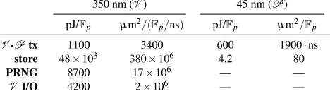
350 nm (V) 45 nm (P)
pJ/Fp µm2/(Fp/ns) pJ/Fp µm2/Fp
V-Ptx 1100 3400 600 1900·ns
store 48×103 380×106 4.2 80
PRNG 8700 17×106 — —
V I/O 4200 2×10⁶ — —
FIGURE7—Costs for communication, storage (including decryption, forV; §4), and PRNG; extrapolated from published results [27, 66, 68, 75, 79, 87, 89, 93, 97, 109] using standard scaling models [67].
here is to characterize Zebra over a wide range of ACs. Thus, we leverage the analytical cost model described in Section 5. We do so in three steps.
First, we obtain values for the parameters of this model by combining synthesis results with data published in the litera-ture (§7.1). Second, we validate the cost model by comparing predictions from the model with both synthesis results and cycle-accurate simulations; these data closely match the an-alytical predictions (§7.2). Third, we estimate the baseline’s costs (§7.3) and then use the validated cost model to measure Zebra’s performance relative to the baseline, across a range of arithmetic circuit and physical parameters (§7.4).
7.1 Estimating cost model parameters
In this section, we estimate the energy, area, and delay of Zebra’s basic operations (§5, (1)–(6)).
Synthesis of field operations. Figure 6 reports synthesis data for both field operations inFp,p=261−1, which admits an
ef-ficient and straightforward modular reduction. Both operations were written in Verilog and synthesized to two technology li-braries: Nangate 45 nm Open Cell [8] and a 350 nm library from NC State University and the University of Utah [9]. For synthesis, we use Cadence Encounter RTL Compiler [3].
Communication, storage, and PRNG costs. Figure 7 re-ports area and energy costs of communication, storage, and ran-dom number generation using published measurements from built chips. Specifically, we use results from CPUs built with 3D packaging [75, 79], SRAM designs [89], solid-state stor-age [53, 93], ASICs for cryptographic operations [66, 68, 109], and optical interconnects [27, 87, 97].
For all parameters, we use standard CMOS scaling models to extrapolate to other technology nodes for evaluation.9
9A standard technique in CMOS circuit design is projecting how circuits will
scale into other technology nodes. Modeling this behavior is of great practical interest, because it allows accurate cost modeling prior to designing and fabricating a chip. As a result, such models are regularly used in industry [67].
logG measured predicted error
area 4 8.76 9.42 +7.6%
(mm2) 5 17.06 18.57 +8.8%
6 33.87 36.78 +8.6%
7 66.07 73.11 +11%
delay 4 682 681 -0.2%
(cycles) 5 896 891 -0.6%
6 1114 1115 +0.1%
7 1358 1353 -0.4%
+,×ops 4 901, 1204 901, 1204 0%
5 2244, 3173 2244, 3173 0%
6 5367, 8006 5367, 8006 0%
7 12494, 19591 12494, 19591 0%
FIGURE 8—Comparison of cost model (§5) with measured data. Area numbers come from synthesis; delay and operation counts come from cycle-accurate RTL simulation.
7.2 Validating the cost model
We use synthesis and simulation to validate the cost model (§5). To measure area, we synthesize sub-provers (§3.1) for AC lay-ers over several values ofG. To measure energy and through-put, we perform cycle-accurate RTL simulations for the same sub-provers, recording the pipeline delay (§5, Fig. 5) and the number of invocations of field addition and multiplication.10
Figure 8 compares our model’s predictions to the data ob-tained from synthesis and simulation. The model predicts slightly greater area than the synthesis results show. This is likely because, in the context of a larger circuit, the synthesizer has more information (e.g., related to critical timing paths) and thus is better able to optimize the field arithmetic primitives.
Although we have not presented our validation ofV’s costs, its cost model has similar fidelity.
7.3 Baseline: native trusted implementations
For an arithmetic circuit with depthd, widthG, and a fraction δ of multiplication gates, we estimate the costs of directly executing the AC in the trusted technology node. To do so, we devise an optimization procedure that minimizesA/T (under the constraint that total area is limited to someAmax; §2.3). Since this baseline is a direct implementation of the arith-metic circuit, we accountEas the sum of the energy for each operation in the AC, plus the energy for I/O (§4).
Optimization proceeds in two steps. In the first step, the procedure apportions area to multiplication and addition prim-itives, based onδ and on the relative time and area cost of each operation. In the second step, the procedure chooses a pipelining strategy that minimizes delay, subject to sequencing requirements imposed byC’s layering.
It is possible, through hand optimization, to exploit the structure of particular ACs in order to improve upon this
8 12 16 20 24 28 32 0.3
1 3
d, depth of arithmetic circuit Performance relative to native baseline (higher is better)
E As/T, s=10 As/T, s=3 As/T, s=1 As/T, s=1/3
(a) Performance vs.d.
6 10 14 18 22
0.3 1 3
log
2 G, width of arithmetic circuit Performance relative to native baseline (higher is better)
E As/T, s=10 As/T, s=3 As/T, s=1 As/T, s=1/3
(b) Performance vs.G.
0.2 0.4 0.6 0.8
0.3 1 3
δ, fraction of multipliers in arithmetic circuit
Performance relative to native baseline (higher is better)
E As/T, s=10 As/T, s=3 As/T, s=1 As/T, s=1/3
(c) Performance vs.δ.
180 250 350 500
0.3 1 3
trusted process technology, nm
Performance relative to native
baseline (higher is better)
E As/T, s=10 As/T, s=3 As/T, s=1 As/T, s=1/3
(d) Performance vs. trusted node.
7 14 22 35 45 0.01
0.03 0.1 0.3 1 3
untrusted process technology, nm
Performance relative to native
baseline (higher is better)
E As/T, s=10 As/T, s=3 As/T, s=1 As/T, s=1/3
(e) Performance vs. untrusted node.
5 20 50 80 110 140 170 200
0.3 1 3
maximum chip area, mm2
Performance relative to native baseline (higher is better)
E As/T, s=10 As/T, s=3 As/T, s=1 As/T, s=1/3
(f) Performance vs. maximum chip area.
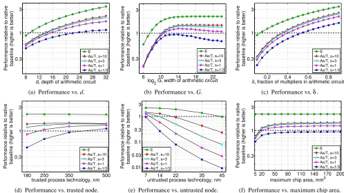
FIGURE9—Zebra performance relative to baseline (§7.3) onEandAs/T metrics (§2.3), varyingC parameters, technology nodes, and maximum chip area. In each case, we vary one parameter and fix the rest. Fixed parameters are: trusted technology node = 350 nm; untrusted technology node = 7 nm; depth ofC,d=20; width ofC,G=214; fraction of multipliers inC,δ=0.5; maximum chip area,Amax=200 mm2; maximum power dissipation,Pmax=150 W. In all cases, designs follow the optimization procedures described in Sections 7.1–7.3.
timization procedure, but our goal is a procedure that gives good results for generic ACs. We note that our optimization procedure is realistic: it is roughly similar to the one used by automated hardware design toolkits such as Spiral [84].
7.4 Zebra versus baseline
This section evaluates the performance of Zebra versus the baseline, on the metricsEandAs/T, as a function ofC
pa-rameters (widthG, depthd, fraction of multiplication gatesδ), technology nodes, and maximum allowed chip size. We vary each of these parameters, one at a time, fixing others. Fixed parameters are as follows:d=20,G=214,δ=0.5, trusted technology node = 350 nm, untrusted technology node = 7 nm, and Amax =200 mm2. We limit Zebra to no more than
Pmax=150 W, which is comparable to the power dissipation of modern GPUs [2, 5], and we varys∈ {1/3,1,3,10}(§2.3). For each design point, we fixV’s area equal to the native baseline area, and setnP,pl=d. We then optimizenP,sc,nV,io, andnV,sc(§5, Fig. 5). To do so, we first setnV,ioandnV,sc to balance delay amongV’s layers (§3.5), and to minimize these delays subject to area limitations. We choosenP,scso thatP’s pipeline delay is less than or equal toV’s.
Figure 9 summarizes the results. In each plot, the break-even point is designated by the dashed line at 1. We observe the following trends:
• AsC grows in size (Figs. 9a, 9b) or complexity (Fig. 9c), Zebra’s performance improves compared to the baseline. • As the performance gap between the trusted and untrusted
technology nodes grows (Figs. 9d, 9e), Zebra becomes increasingly competitive with the baseline, in bothEand
As/T.
• AsGgrows,P’s area increases (§5, Fig. 5), makingAs/T
worse even asEimproves (Fig. 9b). This is evident in the
s=1/3curve, which is highly sensitive toP’s area. • Finally, we note that Zebra’s competitiveness with the
base-line is relatively insensitive to maximum chip area (Fig. 9f).
7.5 Summary
We have learned several things:
Zebra beats the baseline in a narrow but distinct regime.In particular, Zebra requires more than a decade’s technology gap betweenV andP. Zebra also requires that the computation is “hard” for the baseline, i.e., it involves tens of thousands of
op-erations (Figs. 9a, 9b), with thousands of expensive opop-erations per layer (Figs. 9b, 9c). At a high level, the technology gap offsetsP’s proving costs, while “hard” computations allow V’s savings to surpass the overhead of the protocol (§2.2).