IJEDR1403037
International Journal of Engineering Development and Research (www.ijedr.org)3129
Orthogonal Frequency Division Multiplexing Using
Transmitter Band
Ms. Shweta chawhan, Dr.Suchitra Varade
Lecturer, ProfessorElectronics & Telecommunication Department, Priyadarshni college of engineering, Nagpur, india
________________________________________________________________________________________________________
Abstract— Orthogonal Frequency Division Multiplexing (OFDM) is a multi-carrier modulation technique which divides
the available spectrum into many carriers. OFDM uses the spectrum efficiently compared to FDMA by spacing the channels much closer together and making all carriers orthogonal to one another to prevent interference between the closely spaced carriers. The main advantage of OFDM is their robustness to channel fading in wireless environment, but here MB-OFDM transmitter baseband is designing in order to provide high speed for application than OFDM . The objective of this project is to design and implement a baseband of MB-OFDM transmitter on FPGA hardware which provides very high speed for application. This project concentrates on developing Fast Fourier Transform (FFT) and Inverse Fast Fourier Transform (IFFT). The work also includes in designing a mapping module, serial to parallel and parallel to serial converter module. The design uses FFT and IFFT for the processing module which indicate that the processing block contain inputs data. All modules are designed using VHDL programming language and implement using Apex 20KE board. The board is connected to computer through serial port.Input and output data is displayed to computer .Software and tools which used in this project includes VHDLmg Design Entry, Altera and Altera Quartus-II Software tools are used to assist the design process and downloading process into FPGA board while Apex board is used to execute the designed module.
________________________________________________________________________________________________________
I. INTRODUCTION
Multi-Band Orthogonal Frequency Division Multiplexing (MB-OFDM) is a suitable solution to implementation of high speed data transmission in ultra wideband spectrum by dividing the spectrum available into multiple bands. The baseband of transmitter is one of the most important parts in MB-OFDM system.
Fig 1 Concept of an OFDM signal
II. STRUCTURE OF TRANSMITTER BAND
IJEDR1403037
International Journal of Engineering Development and Research (www.ijedr.org)3130
Fig 2 The structure of MB-OFDM TransmitterBasically we are implementing the digital baseband blocks of MB-OFDM and its major components as follows 1. scrambler
2. encoder 3. pucnturer 4. interleaver 5. qpsk And 6. IFFT + ZPS
This project is implemented as system level design in HDL language we will prefer the know language that is VHDL… III. SCRAMBLER
In telecommunications, a scrambler is a device that transposes or inverts signals or otherwise encodes a message at the transmitter to make the message unintelligible at a receiver not equipped with an appropriately set descrambling device. Whereas encryption usually refers to operations carried out in the digital domain, scrambling usually refers to operations carried out in the analog domain. Scrambling is accomplished by the addition of components to the original signal or the changing of some important component of the original signal in order to make extraction of the original signal difficult. Examples of the latter might include removing or changing vertical or horizontal sync pulses in television signals; televisions will not be able to display a picture from such a signal. Some modern scramblers are actually encryption devices, the name remaining due to the similarities in use, as opposed to internal operation.
A scrambler replaces sequences into other sequences without removing undesirable sequences, and as a result it changes the probability of occurrence of vexatious sequences. Clearly it is not foolproof as there are input sequences that yield zeros, all-ones, or other undesirable periodic output sequences. A scrambler is therefore not a good substitute for a line code, which, through a coding step, removes unwanted sequences.
Purposes of scrambling
There are two main reasons why scrambling is used:
It facilitates the work of a timing recovery circuit (see also Clock recovery), an automatic gain control and other adaptive circuits of the receiver (eliminating long sequences consisting of '0' or '1' only).
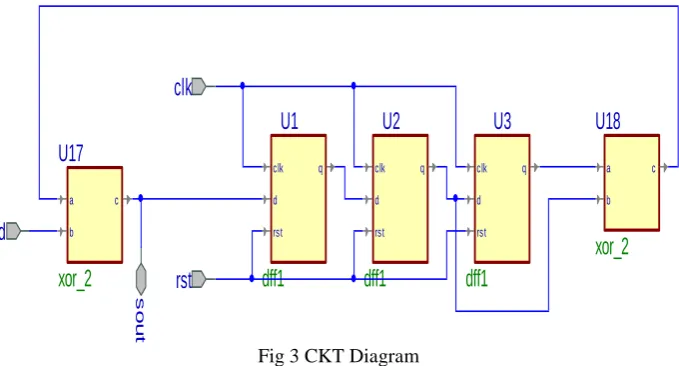
It eliminates the dependence of a signal's power spectrum upon the actual transmitted data, making it more dispersed to meet maximum power spectral density requirements (because if the power is concentrated in a narrow frequency band, it can interfere with adjacent channels due to the cross modulation and the intermodulation caused by non-linearities of the receiving tract). clk q d rst
U1
dff1
clk q d rstU2
dff1
clk q d rstU3
dff1
clk
rst
d
a c bU17
xor_2
s o u t a c bU18
xor_2
IJEDR1403037
International Journal of Engineering Development and Research (www.ijedr.org)3131
Fig 4 ResultFig 5 Simulation of Srambler
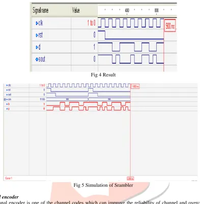
Convolutional encoder
Convolutional encoder is one of the channel codes which can improve the reliability of channel and overcome the effect of noise [8].
Forward error correction (FEC)
Requires that the decoder should also be capable of correcting a certain number of errors, i.e. it should be capable of locating the positions where the errors occurred. Since FEC codes require only simplex communication, they are especially attractive in wireless communication systems, helping to improve the energy efficiency of the system. In the rest of this paper we deal with binary FEC codes only.
Fig 6 TRELLIES Diagram
IJEDR1403037
International Journal of Engineering Development and Research (www.ijedr.org)3132
Convolution encoder can be describe for the back error correction in terms of state table, state diagram and trellis diagram .the state is defined as the contents of the shift register of the encoder. In state table output symbol can be described as a function of input signal and the state. State diagram shows the transition between different state Trellis diagrams is the description of state diagram of the encoder by the time line i.e. represents its time unit with separate states diagram.The encoding sequence 0110 to the forward error correction and then output sequence is 00 11 01 01 it shown by the dark green line in trellis
Fig 7 Result
Fig 8 Simulation of Encoder
The above diagram shows the trellis diagram of Forward error correction it has the state 00, 01.10 and 11 as the encoder is in present state and the switch to next state then the output has been change suppose the encoder has present state is 00 and it is switch to the next state has a clock signal is 0 the output is 00 and it is represented as 0/00. Similarly the output is same state but the clock signal is 1 then output is 11 and it is represented as 1/11. In this way all the state are shows in the trellis diagram… IV. PUCNTURER
IJEDR1403037
International Journal of Engineering Development and Research (www.ijedr.org)3133
Fig 9.Puncturer Ckt• Rst for reset
• Signal1 >> clk source 1 with clk period 25ns • Signal2 >> clk source 2 with clk period 12.5ns
• At each clkin the output switch in between signal1 and signal2
Fig 10.Result
Fig 11.Simulation of Punchturer
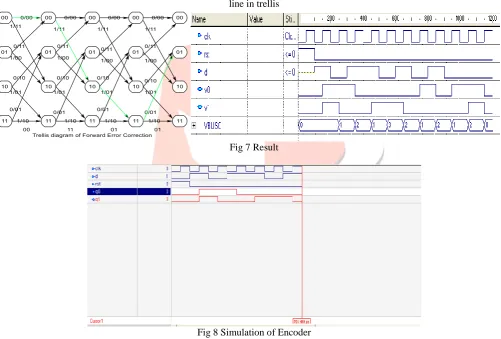
V. INTERLEAVER
An Interleaver is a device that rearranges the ordering of sequence of symbols in a deterministic manner.
QPSk
IJEDR1403037
International Journal of Engineering Development and Research (www.ijedr.org)3134
Fig 12.Stop Fig 13.Pseudo_Ran_Gen
Fig 14.Result sdout(7) <= din(7);
dout(6) <= din(5); dout(5) <= din(2); dout(4) <= din(0); dout(3) <= din(6); dout(2) <= din(1); dout(1) <= din(4); dout(0) <= din(3);
IJEDR1403037
International Journal of Engineering Development and Research (www.ijedr.org)3135
VI. QPSKFig 16.Qpsk
dout1 <= din(7) & din(5) & din(3) & din(1); dout2 <= din(6) & din(4) & din(2) & din(0);
Fig 17.Result
Fig 18.Simulation of Qpsk VII. IFFT
IJEDR1403037
International Journal of Engineering Development and Research (www.ijedr.org)3136
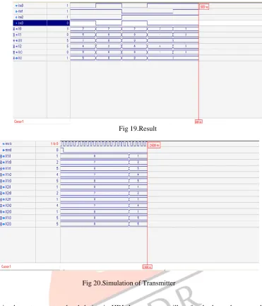
Fig 19.ResultFig 20.Simulation of Transmitter VIII. CONCLUSION
This project will implement as system level design in HDL language we will prefer the know language that is VHDL. In FPGA implementation we have to do both things simulation and FPGA realization in that case /for that there is a need of FPGA kit either xilinx or Altera. Finally after the compilation it will give an generalized information or result regarding total LE [logical elements] consumes which reflects the size [small/large] of the circuit ,RTL view which is nothing but a system overview block diagram, power consumption which is out come of power play analyze tool which is incorporated itself in altera / xilinx , it will give power depending on the switching activity of the signal. Normal power formula is p = c*vdd^2*f where C= total capacitance , which is fix obvious. Vdd = fix supply voltage , which is also fix obvious. F = is switching frequency , which can be control by user.
IX. REFERENCES
[1] Implementation of MB-OFDM Transmitter based on FPGA 978-1-4244-1708-7/08c 2008 IEEE Xu Jinsong, Lu Xiaochun, Wu Haitao, Bian Yujing, Zou Decai, Zou Xiaolong, Wang Chaogang.
[2] Anuj Batra, et al., ―Design of a Multiband OFDM System for Realistic UWB Channel Environments ‖, IEEE TRANSACTIONS ON MICROWAVE THEORY AND TECHNIQUES, VOL. 52, NO. 9, SEPTEMBER 2004.
[3] ISO/IEC, ―Information technology Telecommunications and information exchange between systems — High Rate Ultra Wideband PHY and MAC Standard‖, 26907, Mar.2007, pp 15-59.
[4] J. Balakrishnan, A. Batra, A. Dabak, A multi-band OFDM system for UWB communication, IEEE Conference on Ultra Wideband Systems and Technologies, 2003, pp. 354–358.
[5] Yangheng, et al., ―FPGA / CPLD latest practical technical guidelines‖Tsinghua University Press.2005.pp.1-5..
[6] A. Batra, J. Balakrishnan, A. Dabak, and et al, MultiBand OFDM Physical Layer Proposal for IEEE 802.15.3a,http://www.multibandofdm.org/presentations.html,MultiBand OFDM Alliance SIG, 2004.
[7] A. Batra et al., ―TI physical layer proposal for IEEE 802.15 task group 3a‖,IEEE P802.15-03/142r2-TG3a, Mar. 2003. [8] Wu Weiling,et,al. ―Mobile Communication Principle‖,Publishing house of electronics industry. Beijing,
2005,pp.161-170.