DESIGN AND SIMULATION OF 12T SRAM CELL
USING TRANSMISSION GATE AS ACCESS
TRANSISTOR ON 45 nm TECHNOLOGY
Ravi Kumar
1, Nidhi Sharma
2, Surya Deo Choudhary
31,2,3
ECE Dept, NIET, Greater Noida, UP (India)
ABSTRACT
Technology is contracting down rapidly and almost all the low power gadgets require memory which works
faster, considering that new high speed SRAM cell has been designed. The designed 12T SRAM cells also
consume less power. In our design, transmission gates have been used as access transistors. The Simulation
results such as power dissipation, delay, PDP (Power Delay Product) of the proposed SRAM cell have been
calculated and contrasted with those of some other existing models of SRAM cell. The proposed configuration
gives 61% diminishment in power dissipation. For design and simulation purpose, Tanner EDA Tool V.14.1 at
45nm CMOS has been used.
Keywords:Transmission Gate,Low power Dissipation, Static noise margin, SRAM Swing
voltage,Tanner tool.
I. INTRODUCTION
Decrease in channel length demands an circuit which consume less powerand lessdelay. High speed portable device such as mobile,laptop, CPU demands high speed memory which consume less power and gives high signal to noise margin. ram memory is very important part of any storage circuitry. Dynamic power dissipation and leakage current are the main issues of high speed SRAM cells because this unwanted power dissipation reduces the battery backup life of portable devices. So it is required to have a SRAM cell design, having both low static and dynamic power dissipations.
In this present work a novel low power 12T SRAM cell is proposed. A charge recycling technique is used to minimize the leakage currents and static power dissipation during the mode transitions. Two voltage sources are used at the output nodes to reduce the swing voltages, resulting in reduction of dynamic power dissipation during switching activity. The different performance parameters have been determined for the proposed SRAM cell and compared with those of the other existing SRAM cells.
II. 12T SRAM cell
In order to overcome the problem associated with conventional SRAM cells and other existing SRAM cells, the authors proposes a multi threshold complementary metal oxide semiconductor (MTCMOS) based 12T SRAM architecture to achieve low static and dynamic power dissipations for read and write operations and better stability. In the proposed design two voltage sources V1 and V2 are connected to the outputs of the bit line (BL) and bitbar line respectively. Two NMOS transistors VT1 and VT2 are used, one connected with the BL and the other with the BL directly to switch ON and switch OFF the voltage sources during write operations. The voltage sources reduce the swing voltage during write „0‟ and write „1‟ operation at higher frequencies. This reduction in swing voltage reduces the dynamic power dissipation. The two high threshold voltage (HVT) sleep transistors S1 and S2 are used. NMOS sleep transistor S1 connects node M (also called virtual groundnode) to ground whereas the PMOS sleep transistor S2, connects node N (also called the virtual supply node) to Vdd supply.The low threshold voltage (LVT) transmission gate (TG) is connected between the two virtual nodes M and N for providingcharge sharing. The proposed design is illustrated Sleep transistor control signal (ST) and charge sharing controlsignal (CS) provide the switching activity control on sleep transistors and transmission gate, respectively. Sleep transistorsdisconnect logic
Fig.1The 12T SRAM cell.
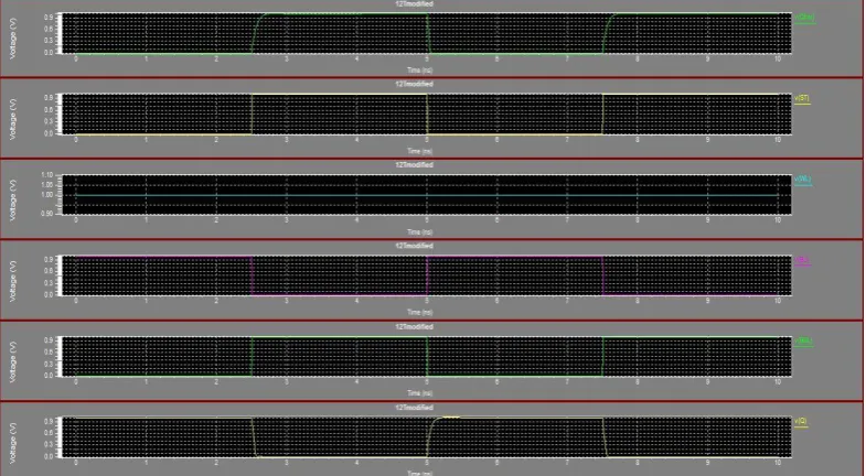
Fig.2 Simulation Diagram of the 12T SRAM cell.
III. PROPOSED 12T SRAM CELL
Fig.3 The proposed 12T SRAM cell.
levels of output as we already know the advantage of TG over MOS. And we can see the effect of these modifications in our results, which are in next section.
Fig.4Simulation Diagram of the proposed 12T SRAM cell.
IV. RESULT
A proposed design is simulated using Tannet EDA Tool using TSMC 45nm technology at 1V supply.fig.4 shows output waveform of proposed 12TSRAM cell. Obtained result of new design is compared with old 12T SRAM cell and tabulated in table 1 as shown.
Designs Power Write 0 Write 1
Delay PDP Delay PDP
12T SRAM 1.9844 uw 21.054 ps 41.780 aJ 22.995 ps 45.632 aj
Proposed 12T SRAM
0.8000 uW 24.227 ps 19.384 aJ 20.921 ps 16.738 aj
Table 1. 12T SRAM vs proposed 12T SRAM cell Comparison
V. CONCLUSION
REFERENCES
[1] Borkar S. Design challenges of technology scaling. IEEE Micro 1999;19(4):23. [2] Brews J. High speed semiconductor devices. New York: Wiley; 1990. pp. 139–210.
[3] Roy K, Prasad SC. Low power CMOS VLSI circuit design. New York: Wiley IntersciencePublications; 2000. p. 27–29.
[4] Taur Y, Ning TH. Fundamentals of modern VLSI devices. New York: Cambridge University Press; 1998. pp. 285–286.
[5] Mostafa H, Anis M, Elmasry M. Adaptive body bias for reducing the impacts of NBTI and process variations on 6T SRAM cells. IEEE Trans CircSyst – I 2011;58(12):2859–71.
[6] K. Tsuchida et al., “A 64Mb MRAM with clamped-reference and adequate-reference schemes,” in Proc. Int. Solid-State Circuits Conf., 2010, pp. 258–259.
[7] M. Hosomi et al., “A novel nonvolatile memory with spin torque transfer magnetization switching: Spin-RAM,” in IEEE Int. Electron Devices Meeting (IEDM) Tech. Dig., 2005, pp. 459–462.
[8] C. J. Lin et al., “45 nm low power CMOS logic compatible embedded STT MRAM utilizing a reverse-connection 1 T/1MTJ cell,” in IEEE Int. Electron Devices Meeting (IEDM) Tech. Dig., 2009, pp. 279– 282.
[9] K. C. Chun et al., “A scaling roadmap and performance evaluation of in-plane and perpendicular MTJ based STT-MRAMs for high-density cache memory,” IEEE J. Solid-State Circuits, vol. 48, no. 2, pp. 598–610, Feb. 2013.
[10] K. Takeuchi, “Scaling challenges of NAND flash memory and hybrid memory system with storage class memory & NAND flash memory,” in Proc. IEEE Custom Integr. Circuits Conf. (CICC), 2013.
[11] D. Halupka et al., “Negative-resistance read and write schemes for STT-MRAM in 0.13 CMOS,” in Proc. Int. Solid-State Circuits Conf., 2010, pp. 256–257.