P a g e | 3801
Wireless Sensor Network Function Composition
Based on Ultra Low Power Digital Circuit
Composition
1
Yeramshetti Ashok Kumar
2T.Krishnarjuna Rao
Assistant Professor , Dept. of ECE Associate Professor, Dept. of ECETKR Colleague of Engineering and Technology Siddhartha Institute of Engineering and Technology Meerpet, Hyderabad, Telangana, India Ibrahimpatnam, Hyderabad, Telangana, India
Abstract: because the CMOS technology continues to scale down
into the nano-scale regime, strength of the circuit with relation to method variation and soft error have become major obstacles for circuit designers. Storage components (SRAM, flip-flops) are unit significantly at risk of method variation and soft errors. Thus, during this work, we've targeted on storage components – to boost the yield loss in SRAM as a result of method variations and to style a soft error tolerant flip-flop. SRAMs area unit significantly at risk of failures as a result of method variation leading to reduced yield. The most drawbacks with SRAM is that the conflicting needs for scan stability and write ability. During this work, we tend to propose styles to beat conflicting trade-off between scan and write stability. Moreover, new SRAM cells, specifically 11TSRAM, PMOS access junction transistor SRAM, area unit projected with capability of performing at near threshold voltages, properly. The impact of body-biasing on SRAM cell is explored to indicate enhancements from body-biasing in sub-threshold regions. Results show a minimum of half-hour improvement in scan noise margin for projected SRAM cells whereas write margin is improved. Moreover, to beat short channel impact, completely different candidate junction transistor structures are investigated to interchange the majority MOSFETs. Among them, FinFET is taken into account to be a promising candidate for scaled CMOS devices in sub-22-nm technology nodes. during this work, by introducing a replacement device, the scan and write stability for SRAM is improved by two hundredth and 11th of September severally, whereas performance is improved by 56%compared to traditional styles.we study the double-gate FinFET SRAM technology-circuit style area to grasp the interaction of device short-channel-effect (SCE), SRAM area, interval, soft error immunity, stability beneath method variations and outpouring.
Keywords: CMOS, SRAM, FinFET, PMOS, VFB, RDF, VLSI,
SERF
1. INTRODUCTION
CMOS devices are scaled down sharply within the previous couple of decades leading to higher integration density and improved performance. However, as a result of short channel effects, threshold voltage (Vth) scaling, compound thickness scaling and exaggerated doping density, the “off” current within the devices has exaggerated drastically with technology scaling. Hence, as we tend to area unit approaching the tip of the Si roadmap, dominant outpouring current is changing into a serious drawback. Moreover, applied mathematics variations in method parameters, like device structure (channel length, compound thickness, width etc), location and variety of do pants in channel (random do pant fluctuation), is increasing with technology scaling. The variation in method parameters leads to giant distribution in delay and outpouring and
considerably reduces strength of a circuit. Hence, giant outpouring current and increasing method variations have emerged as 2 major obstacles for planning CMOS circuits (logic and memory) at the tip of Si roadmap. Smaller transistors area unit inherently quicker and consume less dynamic power. However, once legion transistors area unit integrated along to make a fancy VLSI system, we tend to observe many new challenges threatening the responsibility of computation.
2. DESIGN CHALLENGES IN NANO-SCALE TECHNOLOGY
Leakage Power:
Fig.1 Increasing power over technology generations [Intel]
Fig. 2 leakage power is becoming the dominant component of overall power consumption in scaled technologies
Process Variation: Sub-wavelength lithography has semiconductor diode to giant variation in junction transistor geometries (L;W; TOX) and therefore the flat-band voltage (VFB). method variation effects area unit a lot of rigorous in little size devices. Variations in channel length, channel dimension, compound thickness, threshold voltage, line-edge roughness, and random dopant fluctuations area unit the sources of the inter-die and therefore the intra-die variations in method parameters [the random variations within the variety and site of dopant atoms within the channel region of the device leading to the random variations in junction transistor threshold voltage (RDF)]. one in all this bury die effects is threshold voltage variations as a result of the changes of one junction transistor (e.g. threshold voltage will increase if temperature is reduced). However, intra-die variations could also be completely different from one junction transistor to a different (i.e. increase in Vth for one device on the opposite hand decrease in threshold voltage for another). associate degree example of the systematic intra-die variation may be the modification within the channel length of various transistors of a die that area unit spatially correlate. The RDF elicited Vth variation could be a classic example of the random intra-die variation. Such variations together with higher levels of integration will cause giant unfold in circuit delay, power, and strength across completely different dies (Fig. 2). Therefore, a circuit designed to satisfy a target delay victimisation nominal VTH transistors might not meet the delay target, resulting in constant quantity delay failures. Parameter variations have severe impact (both in terms of errors additionally as leakage) on minimum pure mathematics circuits like SRAM cells. Inter-die parameter variations, plus the intrinsic on-die VTH variation may result in stability failures in SRAM cells, degrading the memory yield.
Power Density and Die-Temperature: Increasing power density as a result of quicker clock, power consumption (due to dynamic power and leakage) and high device integration is changing into another issue. The exaggerated power density interprets into excessive heat whereas the cooling capability of the package remains restricted. Hence, it provides rise to elevation of overall die temperature additionally as localized heating at extremely active regions of a chip (called “hot-spots", Fig..3). historically, a circuit is intended to work at worst-case temperature that is inefficient given the very fact that the circuit might expertise the worstcase condition just for short length. Dynamic thermal management techniques like
logic closure, clock gating, frequency scaling, voltage-frequency asphyxiation etc. are projected in past [3] [4] [5]. though these techniques area unit capable of transferral down power density and temperature, they conjointly degrade the performance significantly. Dynamic voltage scaling may be a good thanks to scale back temperature within the event of warming as a result of it reduces each the switch additionally as outpouring power. However, if the clock frequency isn't scaled at the same time, then exaggerated path delays (due to lower voltage) might result into wrong computation. Combined V-f management technique reduces ends up in three-dimensional profit in terms of power saving at the value of advanced management electronic equipment and pipeline stalls [5]. Nano-scale reliability: As dimensions of MOS devices are scaled down, new responsibility issues area unit returning into impact. one in all these rising responsibility problems is aging effects that end in device performance degradation over time. NBTI (Negative biased temperature instability) could be a well-known aging development that could be a limiting issue for future scaling of devices. NBTI results the generation of treed charges, that cause threshold voltage degradation of PMOS. Another responsibility problems area unit PBTI, Hot carrier injection (HCI), and TDDB that ought to be thought of for ultra-scaled nano-scale devices.
P a g e | 3803 Due to higher field in ultra-thin body (UTB) devices, HCI is
exaggerated considerably that ought to be thought of for future technologies.
3. ULTRA LOW POWER DIGITAL CIRCUIT BLOCKS FOR WIRELESS SENSOR NODES
With the fast development of transportable digital applications, the demand for increasing speed, compact implementation, and low power dissipation triggers varied analysis efforts [7]-[10]. The role of power dissipation in VLSI systems is pervasive. for top performance style, power dissipation may be the limiting issue to clock speed gate density due to the lack to induce power to circuits or to get rid of the warmth that they generate. For transportable data systems, power dissipation contains a direct concerning size, weight, cost, and battery life. Consequently, power dissipation is changing into widely known as a top-priority issue for VLSI circuit style. The challenge facing the VLSI designer is to search out and effectively apply circuit techniques which will balance the wants for performance with those of power dissipation [11]. Thus immoderate low power circuits style becomes the foremost candidate for transportable applications like wireless detector nodes. One common technique for reducing power is power provide scaling. For CMOS circuits the value of lower provides voltage is lower performance. Scaling the edge voltage will limit this performance loss
somewhat however leads to exaggerated leakages [12]. Different techniques employed in low power style embrace clock gating and dynamic voltage/frequency scaling [13], [14]. Sub threshold circuit style involves scaling the availability voltage below the edge voltage, wherever load capacitances area unit charged/discharged by sub threshold outpouring currents. Outpouring currents area unit orders of magnitude less than drain currents within the sturdy inversion regime, thus there's a major limit on the most performance of sub threshold circuits. Therefore, historically, sub threshold circuits are used for applications that need ultra-low power dissipation, with low-to-moderate circuit performance [15]. Within the initial a part of this chapter, completely different topologies for full-adders area unit bestowed together with some circuit modifications to cut back the facility consumption. As a result of the importance of outpouring power consumption in digital CMOS circuits, new technique is projected to cut back the sub-threshold outpouring current in high fan-in gates (e.g. OR gate) and basic blocks like comparators and multiplexers for superior applications. 2 circuit techniques area unit projected to cut back the outpouring current in nano-scale circuits as follows: one. Leakage-tolerant circuit for domino logic two. accommodative provide voltage technique allow us to initial check up on completely different topologies for full-adders
Fig.4. CMOS standard 28T full adder
Table.1 Truth table of SERF full adder design
4. FULL ADDER TOPOLOGIES
during this chapter, we tend to specialise in the total adder topologies such as for sub threshold style and wireless detector networks. one in all the foremost standard full adders is that the customary CMOS full adder that uses twenty eight transistors as shown in Fig. In [16] the sense energy recovery
full adder (SERF) is bestowed. The topology of this circuit is shown in Fig.5 which needs solely ten transistors to implement a full adder.
Fig.5. Different topologies for SERF full adder [17]
Fig.6. Equivalent circuit in input vector ABCin=”110”
Several full adder topologies are bestowed in [18] with an occasional variety of transistors (i.e. little area). However, during this chapter, we tend to specialise in 2 topologies as well as GDI and villein full adders. Let us, first, explore many full adder topologies supported the GDI technique. Then, completely different circuit topologies supported the villein full adder area unit bestowed for immoderate low provide voltage applications. The multi threshold technique is employed to boost the operation of the villein full adder style. The villein style uses solely ten transistors to implement a full adder. though his circuit operates properly at higher provide voltages, if the availability voltage is scaled additional to voltages less than zero.3V, this circuit fails to figure. Table.2.1 describes the behavior of this circuit for various inputs. because it may be seen, the villein adder is confronted with serious issues particularly at lower provide voltages.
5. PROPOSED FULL ADDERS (FA)
P a g e | 3805 will increase the output by Vth, thus we are able to scale the
availability voltage to Vtn+Vtp that's calculable to be less than zero.3V rather than zero.45V for the villein full adder. Another projected plan is as follows: we tend to use a special configuration for the Cout signal and a MUX to provide the add signal of the output of XNOR gate. This topology is shown in Fig. For this circuit Table.2.4 shows that that the logic levels of Cout area unit improved and therefore the overwhelming path in villein is eased. but this circuit uses one junction transistor quite the villein full adder. Another concept considerably improves the operation of the villein style is employing a compound of the techniques projected in Fig. This paper circuit is shown in Fig.5. This circuit permits even a lot of scaling of the availability voltage less than
Fig.7. Output waveforms of GDI#1 and test bench
Vtn+Vtp that is calculable to be zero.3V. moreover, we tend to might use the precise filler to change the circuit to figure at lower provide voltages. This circuit shows far better practicality compared with different villein adder topologies. During this circuit, when A=1, B=1,
Table.2. Power consumption of full adders
Fig.8 GDI #2 full adder circuit
Cin=0, there aren't any problems; as a result of the F node is connected to “1”, that eliminates the facility overwhelming path in Fig. as a result of the gates of the pass transistors area unit connected to VDD, the PMOS junction transistor is off. Moreover, within the state once ABCin=”111”, the F node is connected to VDD, and as a result, add is charged to VDD-Vth and results Cout connecting to VDD. Another circuit could be a new changed GDI primarily based full adder style. The technique is employed to boost the practicality of circuit shown in Fig. for lower provide voltages. The most downside with the GDI full adder is once each x and y inputs area unit at logic low (AB=”00”). Because it may be seen the most drawbacks is with the output of initial stage XNOR gate within the GDI full adder. If we tend to add a circuit to lower the output of initial stage to logic zero rather than Vtp, the matter is resolved. Moreover, the first circuit dissipates a lot of power throughout this state that is currently reduced victimisation projected circuit. The projected GDI full adder is shown in Fig. The side circuit is shown in daring lines in Fig.2.14. Once y and x signals area unit “0”, this activates the side NMOS junction transistor and helps to discharge F node voltage to zero. Thus this alleviates the matter with this circuit represented in Fig2.10. Fig.2.15 shows the waveforms for projected solfa syllable compared to traditional solfa syllable in Fig.2.10. We are able to add another junction transistor to the GDI full adder that's
shown in Fig. during this topology, NMOS junction transistor M2 is side to attach the add signaling to ground once G node voltage is high. This side NMOS junction transistor {m2|M2|money provide} permits this circuit to figure at lower supply voltages. The projected full-adders modify the operation of GDI and villein full adders at terribly low provide voltages. Therefore, we tend to contemplate new GDI full-adders as GDI#1 and GDI#2 and for villein full full-adders by concerning the corresponding figures.
6. SIMULATIONS AND RESULTS
We simulated solfa syllable circuits for various ranges of frequencies from one hundred kilohertz to ten Mc to search out out that circuit performs well. we tend to use the 65nm CMOS customary models from ST electronics. conjointly we tend to simulated these circuits to search out all-time low provide voltages that these circuits area unit ready to work
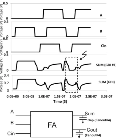
while not failure. The results for all full adders area unit tabulated in Table. to indicate that full adder is best suited to operation in immoderate low provide voltage applications. For villein full adder, the foremost vital downside is its limitation on provide voltage scaling that that can not be reduced below 2Vtn+Vtp. This drawback is tougher in corners particularly in SS corner (Slow NMOS, Slow PMOS). the availability voltage at that villein outputs area unit satisfactory is on top of zero.5V with upsized transistors. The simulation results for various full adder circuits area unit shown in Table. Because it may be seen in Table. The facility consumption for villein full adder is less than different circuits. The availability voltage for this style is proscribed to voltages on top of zero.3V. For these styles we are able to use the lower provide voltages in some cases; however we've to use larger devices that increase the world considerably. to search out the minimum provide voltages for full adder styles, { inputs were applied at different frequency. we tend to thought of the practicality of those circuits in numerous in operation conditions. as an example, because it is shown in Fig. , the dotted region shows the failure in add signal for GDI full adder at zero.3V provide voltage. during this case, for input vector ABCin=”000”, add ought to be at zero logic. however it's discharged simply to zero.16V, which might be assumed as high voltage inflicting a failure in circuit. As Table.2.5 shows, for projected full adder topologies, power consumption is attenuated considerably compared to traditional villein and GDI full adder counterparts. The mail reason of lower power consumption is victimisation the lower provide voltages that cause reduction in dynamic power (quadratic) and conjointly sub threshold
P a g e | 3807 Fig.10. Proposed domino logic circuit-1 [30]
Power consumption (exponential). Table shows the results for delay comparison for projected circuits compared to different topologies in literature. Because it is shown, the projected full adders improve the PDP in some cases by 2X times. For brand new GDI full adder styles, in projected circuits, the PDP is improved compared to traditional GDI full adder circuit [10]. in keeping with junction transistor level simulations, the facility consumption is attenuated with a minimum of sixty two for the villein style and eighty six for the GDI full adder style. The value could be a little space overhead; the projected circuits have atiny low space overhead up to Martinmas compared with villein and GDI full adders. Conjointly the GDI technique showed that this logic may be appropriate for immoderate low power applications. In next section, as a result of the importance of outpouring current mechanisms in immoderate deep submicron technologies, a replacement outpouring tolerant logic circuit is projected. Therefore, allow us to initial check up on completely different sources of noises inflicting lower strength in logic circuit style. As we tend to mentioned in chapter one, for immoderate low voltage applications, In/Ioff magnitude relation decreases considerably. Therefore, by applying some techniques to cut back outpouring current, let say by ten times, Ion/Ioff will increase by ten times, leads to improved performance, power, and strong operation.
REFERENCES
[1]. S. Mukhopadhyay, K. Kang, H. Mahmoodi, and K. Roy, “Design of reliable and selfrepairing SRAM in nano-scale technologies using leakage and delay monitoring," in International Test Conference, p. 10, 2005.
[2]. K. Roy, “Leakage current mechanisms and leakage reduction techniques in deepsubmicron CMOS circuits," in Proceedings of IEEE, pp. 305-327, 2003.
[3]. S. Gunther, F. Binns, D. Carmean, , and J. Hall, “Managing the impact of in-creasing microprocessor power consumption," in Intel Technology Journal, vol. 5,p. 1, 2001.
[4]. K. Skadron, M. R. Stan, W. Huang, S. Velusamy, K. Sankaranarayanan, , and D. Tarjan, “Temperature aware micro-architecture,” in International Symposium on Computer Architecture, pp. 2{13, 2003.
[5]. C. Poirier, R. McGowen, C. Bostak, and S. Naffziger, “Power and temperature control on a 90nm itanium-family processor,” in International Solid State Circuits Conference, vol. 1, pp. 304-305, 2005.
[6]. Seongmoo Heo; Asanovic, K.; , "Load-sensitive flip-flop characterizations," VLSI, 2001. Proceedings. IEEE Computer Society Workshop on , vol., no., pp.87-92, May 2001
[7]. N. Weste and K. Eshraghian, Principles of CMOS digital design.Reading, MA: Addison-Wesley, pp. 304–307.
[8]. A. P. Chandrakasan, S. Sheng, and R. W. Brodersen, “Low- power CMOS digital design,” IEEE J. Solid-State Circuits, vol. 27, pp. 473– 484,Apr. 1992.
[9]. A. P. Chandrakasan and R.W. Brodersen, “Minimizing power consumption in digital CMOS circuits,” Proc. IEEE, vol. 83, No. 4, pp. 498–523, Apr. 1995.
[10].A. Morgenshtein, A. Fish, I. A. Wanger,” Gate-Diffusion Input (GDI):A power efficient method for digital combinational circuits”, IEEE Tran.On Very Large Scale Integration (VLSI), Vol. 10, No. 5, 2002, pp. 566-581.
[11].Moradi, F.; Wisland, D.T.; Tuan Vu Cao; Peiravi, A.; Mahmoodi, H.; , "1-bit sub threshold full adders in 65nm CMOS technology," Microelectronics, 2008. ICM 2008. International Conference on , vol., no., pp.268-271, 14-17 Dec. 2008 2.
[12].Moradi, F.; Wisland, D.T.; Mahmoodi, H.; Berg, Y.; Tuan Vu Cao; , "New SRAM design using body bias technique for ultra low power applications," Quality Electronic Design (ISQED), 2010 11th International Symposium on , vol., no., pp.468-471, 22-24 March 2010 [13].Moradi, F.; Wisland, D.T.; Mahmoodi, H.; Tuan Vu Cao; Zarre Dooghabadi, M.; , "Adaptive supply voltage circuit using body bias technique," Mixed Design of Integrated Circuits & Systems, 2009. MIXDES '09. MIXDES-16th International Conference , vol., no., pp.215-219, 25-27 June 2009
[14].Moradi, F.; Wisland, D.T.; Mahmoodi, H.; Tuan Vu Cao; , "Improved write margin 6T-SRAM for low supply voltage applications," SOC Conference, 2009. SOCC 2009. IEEE International , vol., no., pp.223-226, 9-11 Sept. 2009
[15].Moradi, F.; Wisland, D.; Berg, Y.; Aunet, S.; Tuan Vu Cao; , "Process variations in sub-threshold SRAM cells in 65nm CMOS," Microelectronics (ICM), 2010 International Conference on , vol., no., pp.371-374, 19-22 Dec. 2010
amplifier flip-flop for low power applications," Custom Integrated Circuits Conference (CICC), 2010 IEEE , vol., no., pp.1-4, 19-22 Sept. 2010
[17].Moradi, F.; Wisland, D.T.; Aunet, S.; Mahmoodi, H.; Tuan Vu Cao; , "65NM subthreshold 11T-SRAM for ultra low voltage applications," SOC Conference, 2008 IEEE International , vol., no., pp.113-118, 17-20 Sept. 17-2008
[18].Moradi, F.; Wisland, D.T.; Mahmoodi, H.; Tuan-Vu Cao; , "High speed and leakage-tolerant domino circuits for high fan-in applications in 70nm CMOS technology," Devices, Circuits and Systems, 2008. ICCDCS 2008. 7th International Caribbean Conference on , vol., no., pp.1-5, 28-30 April 2008
[19].Moradi, F.; Wisland, D.T.; Mahmoodi, H.; Peiravi, A.; Aunet, S.; Cao, T.V.; , "New subthreshold concepts in 65nm CMOS technology," Quality of Electronic Design, 2009. ISQED 2009. Quality Electronic Design , vol., no., pp.162-166, 1618 March 2009
[20].Moradi, F.; Wisland, D.T.; Mahmoodi, H.; Aunet, S.; Cao, T.V.; Peiravi, A.; , "Ultra low power full adder topologies," Circuits and Systems, 2009. ISCAS 2009. IEEE International Symposium on , vol., no., pp.3158-3161, 24-27 May 2009
[21].Ali Peiravi, F. Moradi, Dag T. Wisland "Leakage Tolerant, Noise Immune domino logic for circuit design in the ultra deep sub-micron CMOS technology for high fan-in gates" Journal of Applied Science, Volume 24, 2010
[22].F. Moradi, G. Panagopoulos, G. Karakonstantis, H. Mahmoodi, D. Wisland, J. K. Madsen, K. Roy, “ Multi-Level Wordline Driver for Low Power SRAMs in NanoScale CMOS Technology”, Accepted, ICCD 2011
[23].F. Moradi, D. Wisland, H. Mahmoodi, K. Roy, “Asymmetrically-doped FinFET (AD) for low-power robust SRAMs ”, IEEE transactions on Electron Devices (TED), 2011, to appear
[24].Moradi F., Dag T. Wisland, Hamid Mahmoodi, “Process Variations in SubThreshold SRAM Cells " ICM 2010, Egypt
[25].Moradi F., G. Panagopoulos, H. Mahmoodi, D. Wisland, and Kaushik Roy, “ Multi-Level wordline driver for Robust SRAM design in Scaled CMOS Technology”, IEEE Transaction on VLSI Journal (TVLSI) 2011, Accepted
[26].Moradi F., Tuan Vu Cao, Dag T. Wisland, Hamid Mahmoodi "Optimal Body Biasing for Maximizing Circuit Performance in 65nm CMOS" accepted, MWSCAS 2011 Under Review ternational Conference , vol., no., pp.187-192, 25-27 June 2009.
[27].F. Moradi, G. Panagopoulos, D. Wisland, H. Mahmoodi, Kaushik Roy “ FlipFlops for Ultra Low-Power DSP Applications”, IEEE TVLSI, 2011, Final Revision
[28].F.Moradi, D. Wisland, K. Roy “ Asymmetric FinFET 6T-SRAM cell for low power applications”, Submitted to ISQED 2012
[29].F. Moradi, G. Panagopolous, Dag T. Wisland, H. Mahmoodi, Kaushik Roy,” Pulsed-Flip-Flop design for high performance applications”, submitted to ISQED 2012
[30].F. Moradi, I. Vatajelu, T. V. Cao, H. Mahmoodi, D. Wisland, ” Domino Logic Designs for High-Performance and Leakage-Tolerant Applications”, Microelectronics Journal, Under review Papers co-author:
[31].Tuan Vu Cao; Wisland, D.T.; Lande, T.S.; Moradi, F.; , "Low phase-noise VCO utilizing NMOS symmetric load for Frequency-based Delta-Sigma Modulators," Electronics, Circuits, and Systems, 2009. ICECS 2009. 16th IEEE International Conference on , vol., no., pp.767-770, 13-16 Dec. 2009.
[32].Tuan Vu Cao; Wisland, D.T.; Lande, T.S.; Moradi, F.; , "A bulk-controlled ringVCO with 1/f-noise reduction for frequency modulator," Mixed Design of Integrated Circuits & Systems, 2009. MIXDES '09. MIXDES-16th In
About the authors:
1
Yeramshetti Ashok Kumar, He got B.Tech degree from Sree Visvesvaraya Institute of Technology and Science in ECE branch from Mahaboobnagar. He got M.Tech degree from ANURAG Engineering College with VLSI System Design from kodad. He is working as
an ASISTANT PROFESSOR for TKR COLLEAGE OF ENGINEERING AND TECHNOLOGY in the department of ECE. He has 6 years of teaching experience in engineering field. He attended many workshops related to VLSI and Low power VLSI. He published 3 papers in various international journals’ attended many conferences. He has very much interest to do research on VLSI Technology and Design, communication systems and Digital electronics.
2T.Krishnarjuna Rao He got B.Tech
degree from ADAM's Engineering college in ECE branch from khammam.. He got M.Tech degree from ANURAG Engineering College with VLSI System Design from kodad. He is working as an ASSOCIATE PROFESSOR for SIDDHARTHA
INSTITUTE OF
![Fig.1 Increasing power over technology generations [Intel]](https://thumb-us.123doks.com/thumbv2/123dok_us/7751729.1270911/2.595.89.496.93.241/fig-increasing-power-over-technology-generations-intel.webp)