ISSN (Print) : 2320 – 3765 ISSN (Online): 2278 – 8875
I
nternational
J
ournal of
A
dvanced
R
esearch in
E
lectrical,
E
lectronics and
I
nstrumentation
E
ngineering
(An ISO 3297: 2007 Certified Organization)
Vol. 3, Issue 11, November 2014
An Advanced Controller for Improving the
Performance of Single Phase 7-Level Inverter
for Grid Connected PV System
M. Murali Krishna, P. Chandra Babu
PG Scholar, Department of Electrical and Electronics Engineering, QIS Institute of Technology, Ongole, A.P, India Assistant Professor, Department of Electrical and Electronics Engineering, QIS Institute of Technology, Ongole, A.P,
India
ABSTRACT: This paper proposes a fuzzy controller for advancing the performance of a seven level multilevel inverter for grid connected photovoltaic system. This topology gives reduced THD and improved wave shape rather than conventional controlled seven level inverter. Here we are using three identical reference signals (Vref1, Vref2, and
Vref3) with offset value same as amplitude of the triangular carrier (V carrier) signal to generate the PWM signals. Pv
based inverter providing seven levels of output voltage and it recounts the improvement of novel modified H-bridge single phase multilevel inverter, it has two diode bidirectional switches and a novel pulse width modulation technique. By controlling the modulation index, the required number of levels of the inverter’s output voltage can be achieved. This topology is advantages in MPPT system. Multilevel inverter with FUZZY control implementation is advantages in improved output waveform, lover the THD and fast error correction. The proposed system was verified through MAT lab/Simulation program.
KEYWORDS: Fuzzy logic, Micro Grid, MPPT, pulse widthmodulation PWM),photovoltaic(PV) system,and THD. I. INTRODUCTION
1.1 MULTILEVEL INVERTOR
Multilevel inverter technology has emerged recently as a very important alternative in the area of high-power medium-voltage energy control. The popular methods are diode-clamped inverter (neutral-point clamped), capacitor-clamped (flying capacitor), and cascaded multilevel inverters with separate DC sources. The last one is most fusible topology used in all areas. This paper presents the most relevant structure of the multilevel inverter using cascaded-inverters with separated dc sources will be introduced, as well as switching pattern.
1.1.1 Full-bridge or “H-bridge” Voltage Source Inverter
ISSN (Print) : 2320 – 3765 ISSN (Online): 2278 – 8875
I
nternational
J
ournal of
A
dvanced
R
esearch in
E
lectrical,
E
lectronics and
I
nstrumentation
E
ngineering
(An ISO 3297: 2007 Certified Organization)
Vol. 3, Issue 11, November 2014
Figure: 1. An H-bridge cell
1.2 CASCADED H-BRIDGES INVERTER
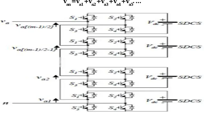
A single-phase structure of an m-level cascaded inverter is illustrated in Figure 1.Each separate dc source (SDCS) is connected to a single-phase H-bridge, inverter. Each inverter level can generate three different voltage outputs, +Vdc, 0, and –Vdc by connecting the dc source to the ac output by different combinations of the four switches,
V
AN Vdc1 Vdc 2 ...Vdc( S 1) VdcS (1.1) S
1, S2, S3, and S4. To obtain +Vdc, switches S1 and S4 are turned on, whereas –Vdc can be obtained by turning on
switches S2 and S3. By turning on S1 and S2 or S3 and S4, the output voltage is 0. The ac outputs of each of the different full-bridge inverter levels are connected in series such that the synthesized voltage waveform is the sum of the inverter outputs. The number of output phase voltage levels m in a cascade inverter is defined by
m = 2s+1,
Where‘s’ is the number of separate dc sources.
An example phase voltage waveform for an m-level cascaded H-bridge inverter with S-SDCSs and S full bridges is shown in Figure 2
van = va1 + va2 + va3 + va4 + va5. …
ISSN (Print) : 2320 – 3765 ISSN (Online): 2278 – 8875
I
nternational
J
ournal of
A
dvanced
R
esearch in
E
lectrical,
E
lectronics and
I
nstrumentation
E
ngineering
(An ISO 3297: 2007 Certified Organization)
Vol. 3, Issue 11, November 2014
II. CONVENTIONAL MULTYLEVAL H- BRIDGE TOPOLOGY
Fig.3 Proposed single-phase seven-level grid-connected inverter for photovoltaic systems.
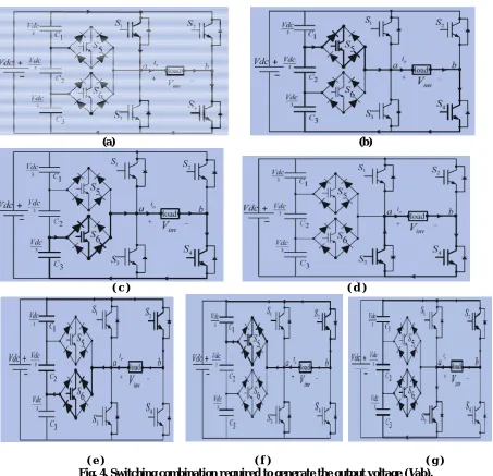
The proposed single-phase seven-level inverter was developed from the five-level inverter. It comprises a single-phase conventional H-bridge inverter, two bidirectional switches, and a capacitor voltage divider formed by C1,
C2,and C3, as shown in Fig. 3. The modified H-bridge topology is significantly advantageous over other topologies, i.e., less power switch, power diodes, and less capacitors for inverters of the same number of levels. Photovoltaic (PV) arrays were connected to the inverter via a dc–dc boost converter. The power generated by the inverter is to be delivered to the power network, so the utility grid, rather than a load, was used. The dc–dc boost converter was required because the PV arrays had a voltage that was lower than the grid voltage. High dc bus voltages are necessary to ensure that power flows from the PV arrays to the grid. A filtering inductance Lf was used to filter the current injected into the grid. Proper switching of the inverter can produce seven output-voltage levels (Vdc, 2Vdc/3, Vdc/3,
0,−Vdc,−2Vdc/3,−Vdc/3) from the dc supply voltage. The proposed inverter’s operation can be divided into seven switching states, as shown in Fig. 4(a)–(g). Fig. 4(a), (d),and (g) shows a conventional inverter’s operational states in sequence, while Fig. 4(b), (c), (e), and (f) shows additional states in the proposed inverter synthesizing one- and two-third levels of the dc-bus voltage. The required seven levels of output voltage were generated as follows.
1) Maximum positive output (Vdc): S1 is ON, connecting the load positive terminal to Vd, And S4 is ON, connecting the load negative terminal to ground. All other controlled switches are OFF; the voltage applied to the load terminals is
Vdc. Fig. 4(a) shows the current paths that are active at this stage.
2) Two-third positive output (2Vdc/3): The bidirectional switch S5 is ON, connecting the load positive terminal and S4 is ON, connecting the load negative terminal to ground.All other controlled switches are OFF; the voltage applied to the load terminals is 2Vdc/3. Fig. 4(b)shows the current paths that are active at this stage.
3) One-third positive output (Vdc/3): The bidirectional switch S6 is ON, connecting the load positive terminal, and S4 is ON, connecting the load negative terminal to ground. All other controlled switches are OFF; the voltage applied to the load terminals is Vdc/3. Fig. 4(c) shows the current paths that are active at this stage.
4) Zero output: This level can be produced by two switching combinations; switches S3 and S4 are ON, or S1 and S2 are ON, and all other controlled switches are OFF; terminal ab is a short circuit, and the voltage applied to the load terminals is zero. Fig. 4(d) shows the current paths that are active at this stage.
ISSN (Print) : 2320 – 3765 ISSN (Online): 2278 – 8875
I
nternational
J
ournal of
A
dvanced
R
esearch in
E
lectrical,
E
lectronics and
I
nstrumentation
E
ngineering
(An ISO 3297: 2007 Certified Organization)
Vol. 3, Issue 11, November 2014
6) Two-third negative output (−2Vdc/3): The bidirectional switch S6 is ON, connecting the load positive terminal, and
S2 is ON, connecting the load negative terminal to ground. All other controlled switches are OFF; the voltage applied to the load terminals is −2Vdc/3. Fig. 4(f) shows the current paths that are active at this stage.
7) Maximum negative output (−Vdc): S2 is ON, connecting the load negative terminal to Vdc, and S3 is ON, connecting the load positive terminal to ground. All other controlled switches are OFF; the voltage applied to the load terminals is −Vdc. Fig. 4(g) shows the current paths that are active at this stage.
(a) (b)
( c ) ( d )
( e ) ( f ) ( g )
Fig. 4. Switching combination required to generate the output voltage (Vab).
ISSN (Print) : 2320 – 3765 ISSN (Online): 2278 – 8875
I
nternational
J
ournal of
A
dvanced
R
esearch in
E
lectrical,
E
lectronics and
I
nstrumentation
E
ngineering
(An ISO 3297: 2007 Certified Organization)
Vol. 3, Issue 11, November 2014
TABLE 1 Output Voltages According To Switches On-Off Condition
Table I shows the switching combinations required to generate out put voltage.
2.1 PWM Modulation
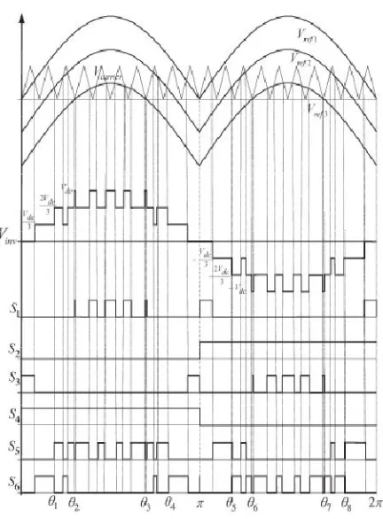
A novel PWM modulation technique was introduced to generate the PWM switching signals. Three reference signals (Vref1, Vref2, and Vref3) were compared with a carrier signal (Vcarrier). The reference signals had the same frequency and amplitude and were in phase with an offset value that was equivalent to the amplitude of the carrier signal. The reference signals were each compared with the carrier signal. If Vref1 had exceeded the peak amplitude of
Vcarrier, Vref2 was compared with Vcarrier until it had exceeded the peak amplitude of Vcarrier. Then, onward, Vref3 would take charge and would be compared with Vcarrier until it reached zero. Once Vref3 had reached zero, Vref2 would be compared until it reached zero. Then, onward, Vref1 would be compared with Vcarrier. Fig. 3 shows the resulting switching pattern. Switches S1, S3, S5, and S6 would be switching at the rate of the carrier signal frequency, whereas S2 and S4 would operate at a frequency that was equivalent to the fundamental frequency.
The phase angle depends on modulation index Ma. Theoretically for a single reference signal and a single carrier signal, the modulation index is defined to be
Ma = Am/Ac (02)
while for a single-reference signal and a dual carrier signal, the modulation index is defined to be
Ma = Am/2Ac. (03)
Since the proposed seven-level PWM inverter utilizes three carrier signals, the modulation index is defined to be
Ma = Am/3Ac (04)
where Ac is the peak-to-peak value of the carrier signal and Am is the peak value of the voltage reference signal Vref . When the modulation index is less than 0.33, the phase angle displacement is
θ1 =θ2 = θ3 = θ4 = π/2 (05)
ISSN (Print) : 2320 – 3765 ISSN (Online): 2278 – 8875
I
nternational
J
ournal of
A
dvanced
R
esearch in
E
lectrical,
E
lectronics and
I
nstrumentation
E
ngineering
(An ISO 3297: 2007 Certified Organization)
Vol. 3, Issue 11, November 2014
Fig. 5. Switching pattern for the single-phase seven-level inverter
Fig. 6. Seven-level output voltage (Vab) and switching angles.
For one cycle of the fundamental frequency, the proposed inverter operated through six modes. Fig. 6 shows the per unit output-voltage signal for one cycle. The six modes are described as follows:
Mode 1 : 0 < ωt < θ1 and θ4 < ωt < π
Mode 2 : θ1 < ωt < θ2 and θ3 < ωt < θ4 Mode 3 : θ2 < ωt < θ3
Mode 4 : π < ωt < θ5 and θ8 < ωt < 2π
Mode 5 : θ5 < ωt< θ6 and θ7 < ωt < θ8 Mode 6 : θ6 < ωt < θ7.
On the other hand, when the modulation index is more than 0.33 and less than 0.66, the phase angle displacement is determined by
θ1 = sin−1(Ac/Am) (07)
θ2 =θ3 = π2 (08)
θ4 =π −θ1 (09)
θ5 =π + θ1 (10)
θ6 =θ7 =3π/2 (11)
θ8 =2π −θ1. (12) If the modulation index is more than 0.66, the phase angle displacement is determined by
θ1 = sin−1(Ac/Am) (13)
θ2 = sin−1(2Ac/Am) (14)
θ3 =π −θ2 (15)
θ4 =π −θ1 (16)
θ5 =π + θ1 (17)
θ6 =π + θ2 (18)
θ7 =2π −θ2 (19)
θ8 =2π −θ1. (20)
ISSN (Print) : 2320 – 3765 ISSN (Online): 2278 – 8875
I
nternational
J
ournal of
A
dvanced
R
esearch in
E
lectrical,
E
lectronics and
I
nstrumentation
E
ngineering
(An ISO 3297: 2007 Certified Organization)
Vol. 3, Issue 11, November 2014
wave. The output voltage consists of five dc-voltage levels. The modulation index is set to be more than 0.66 for seven levels of output voltage to be produced. Three reference signals have to be compared with the triangular carrier signal to produce switching signals for the switches.
III. PROPOSED MULTY LEVAL INVERTER TOPOLOGY
In proposed system the out put of the multilevel inverter is improved with help of advanced controller i.e FUZZY Logic controller.
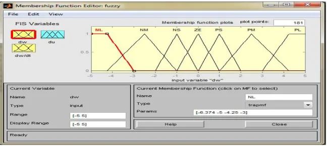
3.1)Fuzzy logic:
In recent years, the number and variety of applications of fuzzy logic have increased significantly. There are five primary GUI tools for building, editing, and observing fuzzy inference systems in the Fuzzy Logic Toolbox. The Fuzzy Inference System or FIS Editor, the Membership Function Editor, the Rule Editor, the Rule Viewer, and the Surface Viewer. the fuzzy controller membership function and its surface view is shown in below fig.7&8.
Fig. 7 Membership function of a fuzzy logic controller
ISSN (Print) : 2320 – 3765 ISSN (Online): 2278 – 8875
I
nternational
J
ournal of
A
dvanced
R
esearch in
E
lectrical,
E
lectronics and
I
nstrumentation
E
ngineering
(An ISO 3297: 2007 Certified Organization)
Vol. 3, Issue 11, November 2014
3.3 ) Proposed FUZZY controller Circuit
Fig. 8 Surface view of FIS editor
VI. COMPARISON of MATLAB /SIMULATION RESULTS
MATLAB SIMULINK simulated the proposed configuration before it was physically implemented in a prototype. The PWM switching patterns were generated by comparing three reference signals (Vref1, Vref2, and Vref3) against a triangular carrier signal (see Fig. 6).
Fig. 6. PWM switching signal generation. Fig. 7. Switching voltages of s1,s2 and s3
ISSN (Print) : 2320 – 3765 ISSN (Online): 2278 – 8875
I
nternational
J
ournal of
A
dvanced
R
esearch in
E
lectrical,
E
lectronics and
I
nstrumentation
E
ngineering
(An ISO 3297: 2007 Certified Organization)
Vol. 3, Issue 11, November 2014
Subsequently, the comparing process produced PWM switching signals for switches S1–S6, as Figs. 7–9 show. One leg of the inverter operated at a high switching rate that was equivalent to the frequency of the carrier signal, while the other leg operated at the rate of the fundamental frequency (i.e., 50 Hz). Switches S5 and S6 also operated at the rate of the carrier signal. Fig. 10. Inverter output voltage (Vinv). Fig. 11. Grid voltage (Vgrid) and grid current (Igrid).of the carrier signal. Fig. 10 shows the simulation result of inverter output voltage Vinv. The dc-bus voltage was set at 300 V (>√2Vgrid; in this case, Vgrid was 120 V). The dc-bus voltage must always be higher than √2 of Vgrid to inject current into the grid, or current will be injected from the grid into the inverter. Therefore, operation is recommended to be between Ma = 0.66 and Ma = 1.0. Vinv comprises seven voltage levels, namely, Vdc, 2Vdc/3,
Vdc/3, 0, −Vdc, −2Vdc/3, and −Vdc/3.The current flowing into the grid was filtered to resemble a pure sine wave in phase with the grid voltage see Fig. 11). As Igrid is almost a pure sine wave at unity power factor, the total harmonic distortion (THD) can be reduced compared with the THD.
Fig.10. Proposed inverter out put voltage (Vinv). Fig. 11. Grid voltage (Vgrid) and grid current (Igrid).
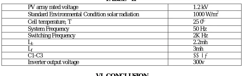
V. MULTILEVEL INVERTER SPECIFICATIONS AND CONTROLLER PARAMETERS.
The below table depicts the specifications and parameters of the inverter
TABLE - II
PV array rated voltage 1.2 kV
Standard Environmental Condition solar radiation 1000 W/m2
Cell temperature, T 25 0C
System Frequency 50 Hz
Switching Frequency 2K Hz
Lb 2.2mh
Lf 3mh
C1-C3 220μF
Inverter output voltage 300v
VI. CONCLUSION
7 level Multilevel inverters offer improved output waveforms and lower THD. This paper has presented a novel PWM switching scheme for the proposed multilevel inverter. It utilizes three reference signals and a triangular carrier signal to generate PWM switching signals. The behavior of the proposed multilevel inverter was analyzed in detail. A FUZZY control is implemented to optimize the performance of the inverter. By controlling the modulation index, the desired number of levels of the inverter’s output voltage can be achieved. The less THD in the seven-level inverter compared with that in the five- and three-level inverters is an attractive solution for grid-connected PV inverters.
REFERENCES
ISSN (Print) : 2320 – 3765 ISSN (Online): 2278 – 8875
I
nternational
J
ournal of
A
dvanced
R
esearch in
E
lectrical,
E
lectronics and
I
nstrumentation
E
ngineering
(An ISO 3297: 2007 Certified Organization)
Vol. 3, Issue 11, November 2014
[2] S. B. Kjaer, J. K. Pedersen, and F. Blaabjerg, “A review of single-phase grid connected inverters for photovoltaic modules,” IEEE Trans. Ind. Appl., vol. 41, no. 5, pp. 1292–1306, Sep./Oct. 2005.
[3] P. K. Hinga, T. Ohnishi, and T. Suzuki, “A new PWM inverter for photovoltaic power generation system,” in Conf. Rec. IEEE Power Electron. Spec. Conf., 1994, pp. 391–395.
[4] Y. Cheng, C. Qian, M. L. Crow, S. Pekarek, and S. Atcitty, “A comparison of diode-clamped and cascaded multilevel converters for a STATCOM with energy storage,” IEEE Trans. Ind. Electron., vol. 53, no. 5, pp. 1512– 1521, Oct. 2006.
[5] M. Saeedifard, R. Iravani, and J. Pou, “A space vector modulation strategy for a back-to-back five-level HVDC converter system,” IEEE Trans. Ind. Electron., vol. 56, no. 2, pp. 452–466, Feb. 2009.
[6] S. Alepuz, S. Busquets-Monge, J. Bordonau, J. A. M. Velasco, C. A. Silva, J. Pontt, and J. Rodríguez, “Control strategies based on symmetrical components for grid-connected converters under voltage dips,” IEEE Trans. Ind. Electron., vol. 56, no. 6, pp. 2162–2173, Jun. 2009.
[7] J. Rodríguez, J. S. Lai, and F. Z. Peng, “Multilevel inverters: A survey of topologies, controls, and applications,” IEEE Trans. Ind. Electron., vol. 49, no. 4, pp. 724–738, Aug. 2002.
[8] J. Rodriguez, S. Bernet, B. Wu, J. O. Pontt, and S. Kouro, “Multilevel voltage-source-converter topologies for industrial medium-voltage drives,” IEEE Trans. Ind. Electron., vol. 54, no. 6, pp. 2930–2945, Dec. 2007.
[9] M. M. Renge and H. M. Suryawanshi, “Five-level diode clamped inverter to eliminate common mode voltage and reduce dv/dt in medium voltage rating induction motor drives,” IEEE Trans. Power Electron., vol. 23, no. 4, pp. 1598–1160, Jul. 2008.
[10] E. Ozdemir, S. Ozdemir, and L. M. Tolbert, “Fundamental-frequencymodulatedsix-level diode-clamped multilevel inverter for three-phase stand-alone photovoltaic system,” IEEE Trans. Ind. Electron., vol. 56,no. 11, pp. 4407–4415, Nov. 2009.
[11] R. Stala, S. Pirog, M. Baszynski, A. Mondzik, A. Penczek, J. Czekonski, and S. Gasiorek, “Results of investigation of multicell converters with balancing circuit—Part I,” IEEE Trans. Ind. Electron., vol. 56, no. 7, pp. 2610–2619, Jul. 2009.
[12] R. Stala, S. Pirog, M. Baszynski, A. Mondzik, A. Penczek, J. Czekonski, and S. Gasiorek, “Results of investigation of multicell converters with balancing circuit—Part II,” IEEE Trans. Ind. Electron., vol. 56, no. 7, pp. 2620–2628, Jul. 2009.
[13] P. Lezana, R. Aguilera, and D. E. Quevedo, “Model predictive control of an asymmetric flying capacitor converter,” IEEE Trans. Ind. Electron., vol. 56, no. 6, pp. 1839–1846, Jun. 2009.
[14] M. F. Escalante, J.-C. Vannier, and A. Arzandé, “Flying capacitor multilevel inverters and DTC motor drive applications,” IEEE Trans. Ind. Electron., vol. 49, no. 4, pp. 809–815, Aug. 2002.
[15] A. Shukla, A. Ghosh, and A. Joshi, “Static shunt and series compensations of an SMIB system using flying capacitor multilevel inverter,” IEEE Trans. Power Del., vol. 20, no. 4, pp. 2613–2622, Oct. 2005.
[16] J. Huang and K. A. Corzine, “Extended operation of flying capacitor multilevel inverter,” IEEE Trans. Power Electron., vol. 21, no. 1, pp. 140– 147, Jan. 2006.
[17] F. Z. Peng, “A generalized multilevel inverter topology with self voltage balancing,” IEEE Trans. Ind. Appl., vol. 37, no. 2, pp. 611–617, Mar./Apr. 2001.
[18] E. Villanueva, P. Correa, J. Rodríguez, andM. Pacas, “Control of a singlephase cascaded H-bridge multilevel inverter for grid-connected photovoltaic systems,” IEEE Trans. Ind. Electron., vol. 56, no. 11, pp. 4399– 4406, Nov. 2009.