Simple Single Phase Five Level Inverter for
PV Applications
A.Nouaiti
1, A.Saad
2, M.Khafallah
3, A.Mesbahi
4, K.Chikh
5PhD Student, Dept. of Electrical, ENSEM, Casablanca, Morocco1 Professor, Dept. of Electrical, ENSEM, Casablanca, Morocco2 Professor, Dept. of Electrical, ENSEM, Casablanca, Morocco3 Assistant Professor, Dept. of Electrical, ENSEM, Casablanca, Morocco4
Assistant Professor, Dept; of Electrical, EST Beni-Mellal, Morocco5
ABSTRACT: This paper presents an analysis and a design of a simple single phase five level inverter for PV applications. The system is composed of a dc-dc multilevel boost converter which is used for generating two voltages at its output terminal. In addition a multilevel inverter suitable for the generated dc bus voltages. The inverter generates five levels at its output terminal. The proposed topology has the advantages of using less number of components, less harmonics, and high efficiency. This is verified through simulation using MATLAB/SIMULINK. The hardware is implemented with multilevel boost converter and multilevel inverter. The results obtained through simulation are verified with hardware results obtained.
KEYWORDS: Multilevel boost converter, Multilevel inverter, PWM, MATLAB/SIMULINK, total harmonic distortion (THD).
I.INTRODUCTION
The demand for renewable energy has increased significantly over the years because of shortage of fossil fuels and greenhouse effect. Among various types of renewable energy sources, solar energy and wind energy have become very popular and demanding due to advancement in power electronics techniques [1].
Multilevel inverter technology has emerged recently as a very important alternative in PV systems. Researchers are going on to improve their capabilities further through optimized control techniques, and to minimize both component count and manufacturing cost [2].
Multilevel inverters started with the neutral point clamped inverter topology [3] [4], and nowadays several multilevel topologies have been developed [5] [6] [7] , but as the output voltage levels increases, it also increases the number of switches, number of independent dc sources, switching stresses, losses, voltage unbalancing across capacitors.
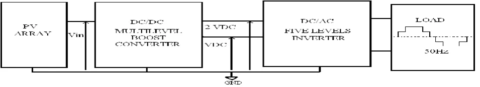
This paper proposes a simple structure for converting DC energy to AC energy for PV applications with less number of switches. The proposed topology is shown in Fig 1.
Block diagram is composed of the DC source (PV array), the multilevel DC–DC boost converter, the DC–AC (five levels) inverter, and the load. The function of the multilevel DC– DC boost converter is to transfer multilevel DC energy to the inverter from single DC source, whereas that of the inverter is to convert the input levels DC energy into an output AC form.
This paper is organized as follows: the multilevel boost converter configuration is presented in Section III, the proposed single phase five levels inverter in Section IV, analysis of output voltages and harmonics in Section V, the hardware implementation in Section VI and Section VII is the conclusion.
II. LITERATURE SURVEY
Title: Simple Control Techniques for Multilevel Inverter
Author: Maha G. Elsheikh, Mahmoud A. Sayed, M. Ahmed, and M. Orabi.
Publish: 34th International Telecommunications Energy Conference (INTELEC), IEEE, 2012.
This paper presents new simple control techniques for single-phase five-level Pulse Width Modulation (PWM) inverter. The proposed control technique requires only driving two high frequency switches with maintain other switches at line frequency. Operational principles with switching functions are analyzed for the two techniques. A comparison between the two proposed techniques has been done based on the resulted features.
Title: Low-Cost Single-Phase Multi-Level Inverter for Grid-Tie PV System Applications
Author: Maha G. Elsheikh, Mahmoud A. Sayed, M. Ahmed, M. Orabi,Afef B. Abdelghani, and Ilhem S. Belkhodja.
Publish: 35th International Telecommunications Energy Conference (INTELEC), IEEE, 2013.
Most renewable energy sources such as photovoltaic, fuel cell, and wind energy generate their power at very low dc voltage which is not suitable for grid connection directly without using transformer. This paper proposes a new high efficient PV grid-tie system. The proposed system consists of a single-phase five-level inverter linked with DC-DC multilevel boost converter used to extract the maximum power from the PV arrays. The proposed inverter has the advantages of using less number of components, low cost, less harmonic, and high efficiency compared to the conventional one.
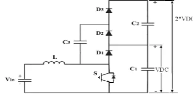
III. MULTILEVEL BOOST CONVERTER.
Fig. 2 shows two levels boost converter, which is based on one inductor, one switch, 3 diodes and 3 capacitors .It, is a boost converter PWM controlled and is able to maintain the same voltage in the two output levels and control the input current. The output voltage can be formulated as follows [8] [9]:
Vout =N ∗ Vin (1 − D)
N is the number of level, D is the duty cycle, Vin is the input voltage and Vout is the output voltage.
Due to the self balanced voltage levels, this topology is suitable to be integrated with the multilevel inverter.
When switch S is conducting, inductor L is charged by input voltage Vin. Capacitor C3 is charged by capacitor C1 through D2. Fig 3
VL=Vin and VC1= VC3. (1)
Fig. 3 Switch-on states.
When S is not conducting, capacitor C1 is charged by input voltage Vin and voltage across inductor L through D1. When D3 is forward biased, capacitors C1 and C2 are charged by Vin, inductor voltage and voltage across C3 through D3. Fig 4
VL= Vin – VC1 and VC3=VC2. (2)
Fig. 4 Switch-off states. For a D duty cycle: VL*D + VL*(1-D) = 0.
From (1) and (2): Vin*D + (Vin-VC1)*(1-D) = 0. VC1 = VDC = Vin
(1−D) and 2*VDC = VC1 + VC2 = 2∗Vin
(1−D)
IV. PROPOSED SINGLE PHASE FIVE LEVEL INVERTER:
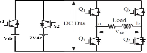
The proposed single phase five level inverter shown in fig 5 modified from [10] [11], consist of a full-bridge (Q1, Q2; Q3, Q4) configuration with two voltage source (Vdc, 2Vdc), and two switches (S1, S2).
The DC Bus has two states by controlling S1 and S2 with a complementary pulses. The H-bridge inverter is used to convert the dc Bus voltage to an ac voltage using conventional PWM.
Two methods have been proposed for obtaining the switching signals for the proposed inverter. Method I:
In this method the pulse with modulation (PWM) control algorithm consist of two triangular carrier signals identical to each other with an offset equivalent to the amplitude of the triangular carrier signal and having the same frequency and are in-phase which compare with reference signal ( which is rectified sinusoidal) as shown in Fig 6.
Fig 6.First PWM strategy (Method I) Method II:
The second proposed method can be implemented by comparing four triangular carrier signals identical to each other with an offset equivalent to the amplitude of the triangular carrier signal and having the same frequency with reference sinusoidal signal as shown in Fig 7.
Fig 7.Second PWM strategy (Method II)
The first method introduces more simplicity into the system. The modulation index for this method is: MI = AM
2AC
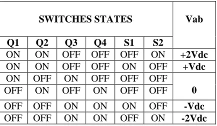
Where AM is the amplitude of reference signal and AC is the amplitude of triangular carrier signal. Table 1 shows the switching states of switches with corresponding voltage level.
Table 1: Switching patterns of the proposed inverter.
SWITCHES STATES Vab
Q1 Q2 Q3 Q4 S1 S2
ON ON OFF OFF OFF ON +2Vdc
ON ON OFF OFF ON OFF +Vdc
ON OFF ON OFF OFF OFF
0
OFF ON OFF ON OFF OFF
OFF OFF ON ON ON OFF -Vdc
V. SIMULATION RESULTS
The proposed system has been simulated by using MATLAB/SIMULINK with resistive charge (R= 30Ω), inductive charge (R= 30Ω, L= 60mH, cos φ = 0.85), input voltage 30V and a duty cycle D=0.8 for the two levels boost converter. Frequency of output voltage is set to 50Hz. Fig 8 shows the SIMULINK model of the proposed topology.
Fig.8. SIMULINK model of the proposed system
For a modulation index MI=0.8, the output voltage and current waveforms for the resistive charge is shown in Fig 9-a, and for the inductive charge is shown in Fig 9-b.
Fig 9-a. Output waveforms for the resistive charge
In the Fig 9-a, the output voltage shows exact 5 levels, and the output current has the same waveform of the voltage because the use of resistive charge.
Fig 9-b. Output waveforms for the inductive charge
For a modulation index MI=1.2, the output voltage and current waveforms for the resistive charge is shown in Fig 10-a, and for the inductive charge is shown in Fig 10-b.
Fig 10-a. Output waveforms for the resistive charge
Fig 10-b. Output waveforms for the inductive charge
Fig 10-a, and 10-b show the influence of the modulation index on output waveforms compared to Fig 9-a, and 9-b.
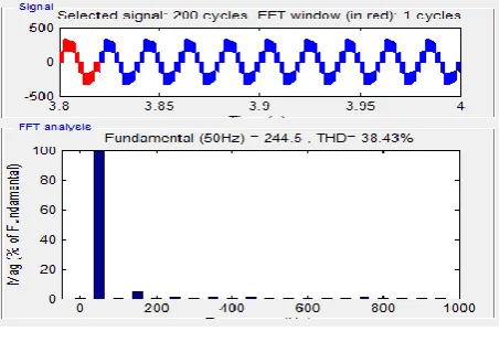
Fig 11 shows the FFT analysis for harmonic component of the output voltage of the inverter for modulation index MI=0.8.
Fig.11. Output voltage THD of the proposed inverter
VI. HARDWARE IMPLEMENTATION
The hardware setup for the proposed topology is developed and implemented with resistive and inductive charge. A microcontroller was used to generate the gate pulse for switches. The experimental results are tested by using a digital storage oscilloscope.
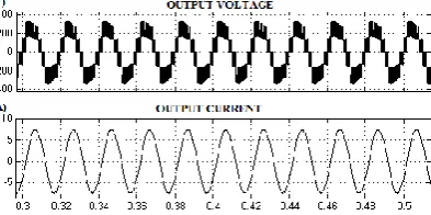
The output voltage and current waveforms for a resistive charge is shown in Fig 12-a, and for inductive charge is shown in Fig 12-b.
Fig 12-a. Output waveforms for the resistive charge
In the Fig 12-a, the output voltage shows exact 5 levels, and the output current has the same waveform of the voltage because the use of resistive charge.
Fig 12-b. Output waveforms for the inductive charge
In Fig 12-b, the output voltage shows exact 5 levels, and the output current has a sinusoidal waveform because the use of inductive charge.
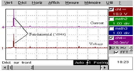
Fig 13 shows the FFT analysis for harmonic component of the output waveforms.
THD of the output voltage and current is measured and found as shown in theFig.13.The inverter produces five level with less harmonic distortion and high efficiency.
From the experimental results it is clear that the hardware setup is working and produces the desired output.
VII.CONCLUSION
This paper deals with the design and implementation of single-phase five-level inverter for a resistive and inductive charge. To generate a 5-level output voltage, the proposed multilevel inverter requires a single dc voltage source. The PWM control technique used here is very simple and helps in reducing the THD. The results shows that the developed multilevel inverter has many merits such as reduce number of switches lower EMI, less harmonic distortion. Thus the proposed inverter can be a good candidate, which can be used in place of conventional PWM inverters in the power rating of a common use.
REFERENCES
[1] V.Srimaheswaran, R.Uthirasamy, “Cascaded Multilevel Inverter for PV Cell Application Using PIC Microcontroller,” International Journal of
Innovative Technology and Exploring Engineering, vol. 2, no. 3, pp.19-24, February 2013.
[2] C.Venugopal, S.Mathew, “A Single Source Five Level Inverter with Reduced Number of Switches,” International Journal of Advanced
Research in Electrical Electronics and Instrumentation Engineering, vol.4, no. 5, May 2015.
[3] A.Nabae, I.Takahashi, H.Akagi, “A new neutral-point clamped PWM inverter,” Industry Applications, IEEE Transactions, vol.IA-17, no 5,
pp.518-523, Sept. 1981.
[4] G.Gopal, B.Shankaraiah, M.Chinnalal, K.Ganesh, G.Satyanarayana, D. Naik, “A new topology of Single-Phase Seven-Level Inverter with
Less Number of Power Elements for Grid Connection,” International Journal of Innovative Technology and Exploring Engineering, vol.3, no.4,September 2013.
[5] M.Pharne, N.Bhosale, “A Review on Multilevel Inverter Topology,” International Conference on Power, Energy and Control (ICPEC), IEEE,
pp.700-703, Feb 2013.
[6] P.Vishvakarma, S.Singh, T. Shukla, “Multilevel Inverters and its Control Strategies: A Comprehensive Review,” 2nd International Conference
on Power, Control and Embedded Systems (ICPCES), IEEE, Dec 2012.
[7] K.Kumar, S.Jain, “Comprehensive review of a recently proposed multilevel inverter,” IET Power Electron, IEEE, vol.7, no.3, pp.467-479,
March 2014.
[8] C. Rosas-Caro, M. Ramirez, M.García-Vite, “Novel DC-DC Multilevel Boost Converter,” Power Electronics Specialists Conference, IEEE,
pp. 2146-2151, June 2008.
[9] J. Mayo-Maldonado, R.Salas-Cabrera, J. Rosas-Caro, J. De Leon-Morales, “ Modelling and control of a DC-DC multilevel boost converter,”
Power Electronics, IET,IEEE, vol.4, no.6, pp.693-700, July 2011.
[10] M. Elsheikh, M. Sayed, M. Ahmed, M. Orabi, “Simple Control Techniques for Multilevel Inverter,” 34th International Telecommunications
Energy Conference (INTELEC), IEEE, Sept 2012.
[11] M. Elsheikh, M. Sayed, M. Ahmed, M. Orabi, A. Abdelghani, I.Belkhodja, “Low-Cost Single-Phase Multi-Level Inverter for Grid-Tie PV