DESIGN AND IMPLEMENTATION OF MMIC BASED LOW NOISE
AMPLIFIER CIRCUITRY FOR PASSIVE PROGRAMMABLE
STIMULATOR IMPLANTS
Rinju Pappachan Jagadeesh Kumar P1
1. INTRODUCTION
In a programmable stimulator implants the signal re-ceived by the antenna is very weak. A low noise amplifier is needed to amplify the signal with minimum self-gener-ated noise.
CMOS devices are typically used in low-noise amplifiers in the microwave frequency region. Low power consumption, low cost and easy availability were the main reasons to choose the CMOS process. The use of Monolithic Microwave Integrated Circuit component technology in modern microwave systems is be-coming more and more important. The main reason for this is the ability to achieve small size and weight. It also has advantages in terms of reliability, repeatability of performance and reduction of parasitic. However, the foundry cost is very high and design duration can take three to six months. This makes the pre-manufacturing cost expensive.
Implanted medical devices can be classified into active and passive based on the source of power. Active implants use a battery as the power source but have less implant ability. Whereas a passive implant can derive power from the wireless power transfer at RF. Such implants have restrictions on the amount of power available to them but have great implant ability. Passive implants have less area compared to active implants.
LNA should have a suitable gain (greater than 10dB) and an ultra-low noise figure at a supply voltage of 1V, such that it consumes very low power. It should be stable over the frequency range of 1.7 to 1.9 GHz. The characteristic impedance is chosen as 50. The LNA can be used for a programmable passive implant as the design is optimized for low power, low noise and less size.
2. RELATED WORKS
The need for a Low Noise Amplifier in Wireless im-plants has become a lot more sophisticated as these sys-tems has become mature and more widespread. LNA should minimize the noise figure, provide good input matching, and should have a sufficient gain. Radio Fre-quency (RF) low noise amplifiers have been designed to operate over a range of RF frequencies. In most of the designs, minimizing the noise figure with sufficient gain is given priority. Power consumption is also an important parameter.
Size of LNA is a design constrained because it is de-signed for an implant. So MMIC technology is used. MMICs were originally fabricated using gallium arsenide (GaAs), a III-V compound semiconductor. It has two fun-damental advantages over Silicon (Si), the traditional ma-terial for IC realization: device (transistor) speed and a semi-insulating substrate. Both factors help with the de-sign of high frequency circuit functions. However, the speed of Si-based technologies has gradually increased as transistor feature sizes have reduced and MMICs can now also be fabricated in Si technology. The primary advan-tage of Si technology is its lower fabrication cost com-pared with GaAs. Silicon wafer diameters are larger (typ-ically 8” or 12” compared with 4” or 6” for GaAs) and the wafer costs are lower, contributing to a less expen-sive IC. Indium Phosphide (InP), have been shown to of-fer superior performance to GaAs in terms of gain, higher cut off frequency, and low noise. However, they also tend to be more expensive due to smaller wafer sizes and in-creased material fragility. Silicon Germanium (SiGe) is a Si-based compound semiconductor technology offering higher speed transistors than conventional Si devices but with similar cost advantages. Gallium Nitride (GaN) is also an option for MMICs. Because GaN transistors can operate at much higher temperatures and work at much higher voltages than GaAs transistors, they make ideal power amplifiers at microwave frequencies.[12]
1
Asst.Prof., Department of Electronics Engineering, Model Engineering College, Thrikkakara
International Journal of Latest Trends in Engineering and Technology
Vol.(9)Issue(2), pp.035-041
DOI: http://dx.doi.org/10.21172/1.92.07
e-ISSN:2278-621X
In the last decade, a great effort has been spent by academic and industrial research to investigate the poten-tial of GaN based active devices to realize LNAs. The inherent high linearity and power-handling capabilities of GaN HEMTs could represent a stunning advance to-ward the possibility of fabricating extremely robust and linear LNAs. Several researches on GaN-based LNAs were reported in open literature, both in hybrid and mono-lithic technologies, showing that a high maturity level was reached for applications at least up to Ku-band. In partic-ular, S-, C-, and X-bands are the most targeted frequency ranges because of their historical use for telecommunica-tions, radar, and electronic warfare [2]. As far as hybrid technology is concerned, operating frequencies are nar-rowed down to 3 GHz . In [15], exploiting a GaN HEMT power bar, an extremely high output IP3 of 54 dBm at 2 GHz was demonstrated with 2 dB associated noise figure. Also in [9],the circuit was based on a GaN HEMT power bar, directly bonded into a hybrid microstrip circuit, and the LNA design was oriented toward obtaining an output IP3 over 49 dBm while achieving 15-dB gain and a noise figure not >2 dB at 1.8 GHz. The two-stage GaN HEMT hybrid LNA proposed in [15] was designed to operate up to 3 GHz and to achieve up to 42-dBm output IP3 together with over 12-dB gain and <1.6-dB noise figure. Moving to monolithic technology, and focusing again on linearity as one of the main figures of merit for LNA design, [3] recorded over 51-dBm output IP3 and <3-dB noise figure measured at 2 GHz for an MMIC cascode feedback LNA. Other interesting results were reported in [4], where two MMIC single-stage LNAs, operating at 7 GHz, are fea-tured by over 43-dBm output IP3.
The combination of high peak electron velocity, high electron concentration and low band gap (0.36 eV) in the channel makes InAs/AlSb based high electron mobility transistor (HEMT) a promising device candidate for mi-crowave/ millimeterwave circuits operating at very low power consumption. High-gain and low-noise circuits based on the InAs/AlSb HEMT technology and operat-ing at dc power consumption below 10 mW have been reported. Recent publications have demonstrated that, at 77 K, the InAs/AlSb HEMT shows large improvements in terms of gate leakage current, transconductance, gain and noise figure. [5]
GaAs FET devices are typically used in low-noise am-plifiers in the microwave frequency region where silicon transistors can’t provide the required gain and noise per-formance. There are, however, many applications in the frequency range below 2 GHz where the low noise figures and high gain of GaAs FETs can improve receiver sensi-tivity. Typical applications include low noise amplifiers (LNAs) in the 800 to 900 MHz frequency range for use in cellular telephone and pager applications and spread spec-trum transceiver applications.
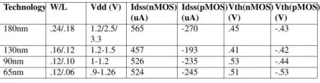
CMOS is the only device which works in 1V supply. The above studied materials will not work in that sup-ply voltage. And hence a comparative study of different CMOS technology is performed.
The frequency of an RF electromagnetic wave can be important in determining how much energy is absorbed and therefore, the potential for harm. The quantity used to characterize this absorption is called “specific absorption rate” or “SAR”. SAR is a measure of the rate of RF energy absorption by the body from the source being measured. SAR provides a straight forward means for
Figure 1: Comparison of various CMOS Technologies.
measuring the RF exposure characteristics of antennas to ensure that they are within the safety guidelines. SAR can also refer to absorption of other forms of energy by tissue, including ultrasound. It is defined as the power absorbed per mass of tissue. The unit of SAR is Watts per Kilogram (W/Kg). SAR is either averaged either over the whole body, or a small sample volume. Local SAR is determined over a mass of 10g.
At a particular frequency, the transmitted power is limited by tissue heating, which is measured by SAR and should not exceed 1.6mW/cm3 as averaged over any 1g of tissue according to the IEEE safety guidelines.
According to IEEE safety guidelines, SAR measures exposure to fields between 3KHz and 300GHz. The value will depend heavily on the geometry of the part of the body that is exposed to the RF energy, and on the exact location and geometry of the RF source.
S. Kim et. al. in Ref [6] explained the wireless power transfer between a source and a weakly coupled implant on the heart. With proper system design, power suffi-cient to operate typical cardiac implants can be received by millimeter-sized coils. From the analysis, the maxi-mum efficiency occurs at about 1.7 GHz and is more than an order of magnitude greater than efficiency in the MHz range.
3. PROPOSED SYSTEM
amplified. While this gives a minimum noise figure, it often results in slightly reduced gain as well as possibility increasing the potential instabil-ities.
3.1 Block Diagram
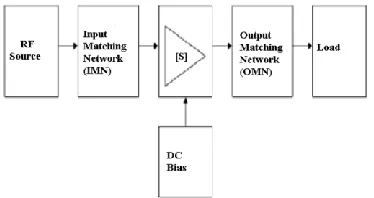
Input to the LNA is from antenna, which is RF signal. The RF signal received by the antenna is needed to be amplified with minimum self-generated noise. There should be a matching between the RF source and the amplifier. And also the output of amplifier is matched with the circuit after that.
Figure 2: System Block Diagram. 3.2 Input Matching Network
The role of the input matching network is to make the input return loss (S11) minimized without introducing additional noise. The interface between the antenna and the LNA entails an interesting issue. Considering the LNA as a voltage amplifier, we may expect that the ideal value of its input impedance is infinite. From the noise point of view, we may require a
transformation network to precede the LNA so as to obtain minimum NF. From signal power point of view, we may utilize conjugate matching between the antenna and the LNA. The input matching network is designed by choosing the source impedance (Zs) equal to the optimum impedance (Zopt). In today’s systems the LNA is designed to have a 50 ohm input impedance.
3.2.1 S parameter
Figure 3: Two Port Network.[13]
Figure 4: S parameter matrix.
The matrix elements S11, S12, S21, S22 are referred to as the scattering parameters or the S-parameters. The parameters S11, S22 have the meaning of reflection coef-ficients, and S21, S12, the meaning of transmission coef-ficients. Rollette’s stability constant K is important to LNA de-sign. Stern Stability factor is defined in terms of s param-eter as:
K =1 + j 4 j2 jS11j2 jS22j2 (1)
2 jS11j jS22j
Where 4=S11S22-S12S21. If K>1 and 4<1 then the circuit is unconditionally stable. Equation (3.1) suggests that stability improves as S12 decreases.
3.3 Amplifier Section
3.4 Conjugate matching
The Figure 5 shows a general amplifier circuit with input and output matching circuits.
Figure 5: Basic transistor amplifier circuit with in-put and output matching networks.
The output matching network is designed by conjugate matching. Conjugate matched condition means that the reflection coefficient of the source ( S) is equal to the conjugate of the input reflection coefficient, in and the reflection coefficient of the load ( L) is equal to the conjugate of the output reflection coefficient, out. This is for maximizing the transducer power gain. i.e. S = in and L = out, where
in =b1=S11+S21S12L (2)
a11 S22 L
out =b2= S22 +S21S12 S (3)
a2 1 S11 S
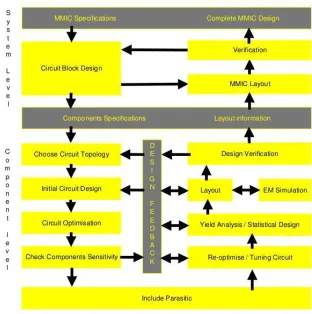
3.5 MMIC Technology
The use of Monolithic Microwave Integrated Circuit com-ponent technology in modern microwave systems is be-coming more and more important. The main reason for this is the ability to achieve small size and weight. It also has advantages in terms of reliability, repeatability of performance and reduction of parasitics. However, the foundry cost is very high and design duration can take three to six months. This makes the pre-manufacturing cost expensive. Moreover, post-fabrication tuning is prac-tically impossible. There are three basic points that should help in order to achieve this goal:
1.A reproducible / stable foundry process.
2.The foundry must provide accurate component mod-els, both active and passive. 3.The use of appropriate design methods.
Factors should be covered about the foundry process are cost of the foundry process, reputation, device perfor -mance, process stability, availability of active and passive structure models
Figure 6: MMIC Design flow chart.[16]
4. IRCUIT ANALYSIS AND DESIGN
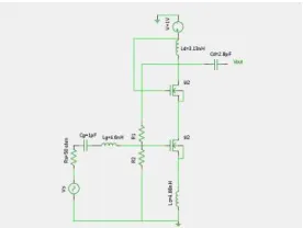
4.1 Cascode Low Noise Amplifier with source degeneration
Figure 7: Cascode LNA with source degeneration.
4.2 Analysis of Cascode stage with source degeneration
Figure 8 shows the input impedance, Zin of the cascade configuration of the Low Noise Amplifier. Figure 8: Input impedance of an inductively degenerated Cascode amplifier.
The input impedance of the Common Source stage is given by:
Zin = s:(Ls + Lg) +1+gm1(Ls) (4)
s:Cgs Cgs
where Cgs is the gate source parasitic capacitance, gm1 is the transconductance of the FET M1. Ls contribute a real term to the input impedance through interaction with Cgs and gm1. By choosing Ls to resonate with Cgs, the impedance will look real at frequencies near the input res-onance. At resonance input impedance is,
Zin= 50 =gm(Ls) (5)
Cgs
Transit frequency (!T ) is given by the equation,
!T = 2 fT =gm (6)
Cgs
The value of source inductance Ls at resonance can be calculated using the equation,
Ls =50 (7)
2 fT
At resonance,
s:(Ls + Lg) + = 0 s:Cgs
Ls + Lg =1 (9)
!2:Cgs
Cgs = 1*10 -10 (10)
Output section at resonance,
s:Ld =1 (11)
s:Cd
4.3 Noise Analysis Of The Cascode Stage
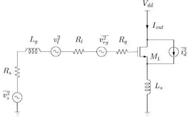
In an RF receiver, the noise contributed by subsequent stages may be neglected if the first stage possess sufficient gain. The noise figure of the Low Noise Amplifier can be approximated using the equivalent circuit in Figure. Elements R1, and Rg represent losses due to inductor resistance and gate resistance, respectively.
Figure 9: Equivalent circuit for input stage noise calculation.
The transconductance of the input stage is given by,
(12)
where Qin, is the effective input Q of the circuit. Rl and Rg, have been neglected relative to Rs. The overall transconductance is apparently independent of gm, the intrinsic device transconductance. The noise figure of the circuit at resonance is given by,
(13)
where Rg ,Rs and Rl are the gate, source, and input (in series with Cgs,) extrinsic ohmic resistances of the FET, respectively. Ro is the generator impedance, gm is the zero-bias drain conductance, !T is the unity current gain bandwidth and is a function of bias and is used to model channel noise for the FET. Rs and ri vary inversely with total device width, WT . Rs and ri substantially contribute to the noise figure.
Input Matching Network
The input matching network is designed using the optimum reflection coefficient �opt. For noise matching,
(14)
Output Matching Network
At the output side, conjugate matching is done. �out is calculated using the equation,
(15)
By making use of smith chart, we can find out the input and output matching networks at a characteristic impedance of Zo = 50Ω.
The passive implants require a LNA with sufficient gain, contribute less noise and consumes as much less power as possible. A 90nm CMOS Cascode amplifier configuration is selected. Simulation is done using ANSOFT Designer .
6. REFERENCES
[1] Goh Fukuda, Satoshi Yoshida, Yuta Kobayashi, Takumasa Noji, Shuntaro Tashiro, And Shigeo Kawasaki, Cryogenic GaAs High Gain and Low Noise Amplifier Module for Radio Astronomy, Proceedings of APMC 2012, Kaohsiung, Taiwan, Dec. 4 -7, 2012
[2] Sergio Colangeli, Andrea Bentini,Walter Ciccognani, Ernesto Limiti, and Antonio Nanni, GaNBased Robust Low-Noise Amplifiers, IEEE Transactions On Electron Devices, Vol. 60, No. 10, October 2013
[3] K. W. Kobayashi, “An 8-W 250-MHz to 3-GHz decade-bandwidth lownoise GaN MMIC feedback amplifier with ¿ + 51-dBm OIP3,” IEEE J. Solid-State Circuits, vol. 47, no. 10, pp. 2316–2326, Oct. 2012.
[4] O. Axelsson and K. Andersson, “Highly linear gallium nitride MMIC LNAs,” in Proc. IEEE Compound Semicond. Integr. Circuit Symp., Oct. 2012, pp. 1–4.
[5] Moschetti. G,Wadefalk .N, Nilsson. P.A, Abbasi, M. ”Cryogenic InAs/AlSb HEMT Wideband Low-Noise IF Amplifier for Ultra-Low-Power Applications ” Microwave and Wireless Components Letters, IEEE (Volume:22 , Issue: 3 ) , Mar. 2012 , pp. 144 – 146
[6] S. Kim, J.S. Ho, L.Y. SChen, and A.S. Poon, ”Wireless power transfer to a cardiac implant”, Applied Physics Letters, Vol. 101, No. 7, pp. 073701-(1-4), August 2012.
[7] Amarjeet Kaur, Himani Malik, Asha Lather and V.K.Lamba, ”Effect of Communication Frequency on Specific bsorption Rate Of Electromagnetic Radiations In Human Body”, International Journal of Soft Computing and Engineering (IJSCE), ISSN:2231-2307, Volume-2, Issue-4, September 2012.
[8] P.Heydari, D.Lin, ”A Performance Optimized CMOS Distributed LNA for UWB Receivers”, Custom Integrated Circuits Conference, IEEE 2005. [9] Philips RF manual, ”Product and design manual for RF small signal discretes”, 2nd Edition. August 2002.
[10] D. Schaeffer and T. Lee, ”A 1.5-V, 1.5-GHz CMOS Low Noise Amplifier”, IEEE journal of Solid-State Circuits, vol. 32, pp. 745-759, May, 1997. [11] mosis website. [Online]. Available: http://www.mosis.com/cgibin/cgiwrap/umosis/swp/params/ibm-90/v15p 9lprf 9lb-params.txt
[12] http://www.ece.rutgers.edu/ orfanidi//ch13.pdf neglected if the first stage possess sufficient gain. The noise
[13] Sunny Gyamlani, Sameena Zafar, Jigisa Sureja and Jigar Chaudhari, ”Comparative Study of various LNA topologies Used for CMOS LNA Design”, Int. J Comp Sci. Emerging Tech, Vol.3 No 1 ,pp. 41-49, February, 2012.
[14] C. Andrei, A. Liero, R. Lossy, W. Heinrich, and M. Rudolph, “Highly linear broadband GaN-based lownoise amplifier,” in Proc. German Microw. Conf., Mar. 2010, pp. 36–38.
[15] P. Chehrenegar, M. Abbasi, J. Grahn, and K. Andersson, “Highly linear 1–3 GHz GaN HEMT low-noise amplifier,” in IEEE Int. Microw. Symp. Dig., Jun. 2012, pp. 1–3.
[16] http://www.armms.org/media/uploads/1326129452.pdf [17] http://www.qsl.net/va3iul/LNA20design.pdf