University of New Hampshire Scholars' Repository
Honors Theses and Capstones
Student Scholarship
Spring 2018
Sensitivity of Black Phosphorus to O2 and
Atmosphere Measured by Macroscopic Four-Point
Probe
Cameron Flynn
University of New Hampshire, Durham, [email protected]
Follow this and additional works at:
https://scholars.unh.edu/honors
Part of the
Condensed Matter Physics Commons
This Senior Honors Thesis is brought to you for free and open access by the Student Scholarship at University of New Hampshire Scholars' Repository. It has been accepted for inclusion in Honors Theses and Capstones by an authorized administrator of University of New Hampshire Scholars' Repository. For more information, please [email protected].
Recommended Citation
Flynn, Cameron, "Sensitivity of Black Phosphorus to O2 and Atmosphere Measured by Macroscopic Four-Point Probe" (2018).
Honors Theses and Capstones. 419.
Four-Point Probe
Cameron Flynn∗ (Dated: Spring 2018)
Scientific interest in black phosphorus, a two-dimensional semiconducting allotrope of phosphorus,
has increased in the last few years, since it was shown in 2014 to have very good properties for
field-effect transistors. Unfortunately, practical use of the material is delayed because of its tendency to
degrade into a phosphoric oxide when left in air. In this thesis I present the effects of atmospheric
air and pure oxygen on the transport properties of bulk black phosphorus with and without light
exposure. For continuous measurements carried out by millimeter-scale four-point probe, we see no
change in the resistance of bulk samples exposed to air and oxygen, with or without light. I argue
that even though we see an intensity shift in the Raman spectroscopy data, indicating oxidation of
the black phosphorus samples, our measured resistances remain constant because the surface layers
are nearly negligible in four-point measurements of bulk crystals. I then show an estimation for
the upper bound of the number of layers affected by degradation as probed by this method, with a
maximum of 900 out of 660,000 total probed layers, or about 0.1%.
∗Electronic address:
Contents
I. Introduction 3
A. An Overview of Black Phosphorus 3
B. Degradation of Black Phosphorus 4
II. Methods 5
A. Chamber and Equipment 5
1. Ultra-High Vacuum Chamber 5
2. Capres Probes 7
3. Probe Design 8
4. Millimeter-Scale Home-Built Probe 9
5. Keithley 2450 SourceMeter 10
6. Battery Box 10
B. Measurement Techniques 11
1. Transport Measurements 11
2. Scanning Tunneling Microscopy 12
3. Raman Spectroscopy 13
C. Experimental Methods 15
1. Air-Free Preparation of Samples 15
2. LabVIEW Programs 16
III. Results 18
A. STM on Black Phosphorus 18
B. Procedural Outline 19
C. Exposure Experiments 19
1. First Low-Pressure Air Exposure Experiment 19
2. Low-Pressure O2Exposure Experiment 20
3. Second Low-Pressure Air Exposure Experiment 20
4. Atmospheric Pressure Air Exposure Experiment 20
D. Raman Spectroscopy on Air-Exposed Sample 22
IV. Discussion 22
V. Conclusion 25
VI. Acknowledgments 26
VII. References 27
VIII. Appendices 28
A. Procedural Appendix 28
1. Landing the Probes 28
2. Testing the Capres Probes 28
3. Approach and Retract Piezo Settings 29
I. INTRODUCTION
A. An Overview of Black Phosphorus
Black phosphorus (BP) has become of interest recently as a two-dimensional material for use in field-effect transistors
because of its physical and electronic properties [1]. It is an allotrope of pure phosphorus that was first discovered
over 100 years ago the same way it is still made, by high pressure and heat applied to white phosphorus past a critical
point in its phase diagram [2]. To make a good transistor, a material must have a high mobility (i.e. charge carriers
such as electrons and holes can move through the material easily) and a high ratio of current during the ‘on’ state
to current during the ‘off’ state, so that random thermal fluctuations do not spur enough electrons into motion to
turn the device on or off. Graphene, the two-dimensional version of graphite, is known for having a high mobility, up
to 200,000 cmV s2 in suspended devices, but has no band gap, so there is no range of voltages (other than exactly zero
volts) for which the device can be off, which leads to a low on/off ratio [3]. Transition metal dichalcogenides (TMDs)
are a class of two-dimensional materials that have band gaps in the optical range, about 1.5-3eV, but low mobilities
(for instance, MoS2, one of the more promising TMDs, has a mobility of only about 200 cm
2
V s [4]). BP has the better
properties of the two classes of materials: the mobility can get up to 10,000 cmV s2, a value less than graphene’s, but
much more than the TMDs. BP also has a non-zero, layer-dependent band gap that goes from 0.3eV in bulk to about
1.5eV in monolayer [5][6]. BP is attractive for optoelectronic applications because these energies correspond to light
in the infrared range, with 800 to 3100nm wavelengths. The band gap in BP is direct, so electron-hole recombination
is uninhibited, another requirement for optoelectronic devices. In addition to these properties, few-layer BP has
been shown to be highly robust against mechanical strain, as repeatedly flexed transistors made of BP showed very
little change in their transfer characteristics after 5000 bending cycles [7]. This property lends itself well to flexible
electronics.
B. Degradation of Black Phosphorus
Black phosphorus may have an optical-range band gap, high carrier mobility, and the ability to be repeatedly flexed
without its electronic properties changing significantly, but unfortunately, it also has the drawback of degrading within
hours when left in air, as shown in figure 2a. However, the mechanism for this degradation reaction is still under
study. In 2015, two theoretical studies came out regarding the degradation of BP. Zilettiet al. did a first-principles
calculation of O2alone with pristine BP. The conclusion they reached with this model is that even in a pristine lattice,
oxygen will chemisorb to the surface of the BP and create hydrophilic patches on what is normally a hydrophobic
surface [9]. Later that year, Uttet al.took this a step further and modeled the interaction of pure O2 on defect sites
[10]. BP has a few types of intrinsic defects, the most prominent being single phosphorus vacancies [11][12]. Uttet al.
showed that on defect sites (including single phosphorus vacancy sites), the energy required for oxygen dissociation
and chemisorption into the lattice was in the range of visible light, as compared to the energy required at pristine
sites, which was in the ultraviolet range, shown in figure 2b [10]. Between these two studies we can see that oxygen
and natural light alone are enough to degrade BP, as long as there are defects. Atmospheric air also contains water, a
polar molecule that could help to degrade the material. Huang, Qiao,et al.in 2016 performed a series of experiments
where BP samples were left in deionized water and in deaerated water (water with all O2 extracted) with light to see
how the degradations compared. What they found was that while flakes still degraded in the deionized water, over two
days there were no changes optically or electronically to monolayer/bilayer samples left in deaerated water. Optical
images from the study are shown in figure 2c. From this they concluded that water and light alone are not enough
to degrade BP, although they speculated that the samples in deionized water degraded faster than they would have
in pure O2, because oxygen chemisorption makes the BP surface hydrophilic, allowing water molecules to aid in the
material degradation [13]. The group in reference [14], Hu, Li, Lei,et al., then tested the hypothesis laid out in [13].
They leaked in humid O2 and humid N2 to BP samples kept in the dark, and found that (by X-Ray Photoemission
Spectroscopy) the samples in humid O2 had developed a phosphoric oxide compound, whereas the samples in humid
N2 had not. What this means is that while light may aid the breakdown of BP in O2, it is not necessary in the
presence of water.
In this thesis, I present a series of experiments that probed the degradation of the electronic properties of BP from
exposure to pure O2 and atmosphere and light, using fixed-geometry four-point probes. The data show that the
electronic properties of bulk BP are unchanged in these experiments. My analysis shows that most of the current
is moving in the crystal interior rather than across the surface, where adsorbed gases would affect the conductivity.
From these results I argue that the degradation reaction (on these timescales) can only be taking place on the first
few layers of the crystal, at maximum 900 out of the 660,000 total probed layers.
II. METHODS
In this section, I present an overview of the equipment used for these experiments along with the reason we used
them. I then present the techniques we used to take data and why each was necessary. Lastly, I give the methodology
for the more technical side projects that were crucial to carry out these experiments.
A. Chamber and Equipment
1. Ultra-High Vacuum Chamber
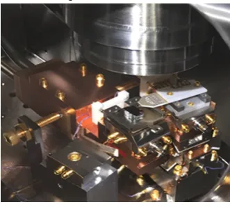
Since BP is air-sensitive, our experiments were conducted inside our ultra-high vacuum chamber, where we could
carefully control exposure to gases. Our UHV chamber was made by RHK Technology. Pictured in figure 3, it is a
figure 3 is the chamber that houses our combined scanning tunneling microscope (STM) and atomic force microscope
(AFM), which are cooled by a closed cycle helium cryostat to about 5K to limit thermal noise. The STM is described
further in section II.B.2. The middle chamber is called the probe chamber and holds a four-point probe (described in
sections II.A.2-4 and II.B.1) and sample stages. The four-point probe stage is controlled by piezomotors for precise
landing. This chamber is outfitted with an evaporator and an ion gun, as well as a leak valve attached to a gas
manifold for in situsurface functionalization. On top is an inverted viewport that houses an optical microscope to
enable probe landing. The small chamber on the left is the load lock, which is how we transfer samples into the
chambers. We feed a positive pressure of nitrogen into this chamber to keep it clean when we load samples in and out.
There are two transfer arms that go between the load lock and the imaging chamber and the imaging chamber and
the probe chamber. Both the imaging and probe chambers are pumped by ion pump and reach about 10−10 mbar.
The load lock is pumped by a turbo pump and can reach the 10−8mbar range.
2. Capres Probes
We initially used micron-scale fixed-geometry four-point probes in these experiments so that we had small, known
cantilever spacing. Capres is the manufacturer of the probes, which are designed to fit inside a micromanipulator for
quick replacement. Due to space limitations inside the UHV chamber, we developed our own base for these probes
(in partnership with RHK Technology) instead of using the micromanipulator (see sections II.A.3-4). The Capres
probes used in this study were five micron and thirty micron probes, named for the distance between the outermost
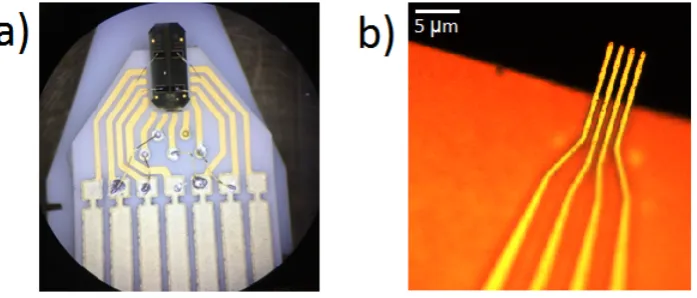
cantilevers (see figure 4b). The five micron probes have four cantilevers that are three microns wide by twenty-five
microns long, and the thirty micron probe cantilevers are six microns wide by thirty microns long. These cantilevers
are made of 1 micron-thick SiO2coated in 25 nanometers of titanium and then 100 nanometers of gold [15]. The gold
continues through the ‘chip’, which is Si as well (shown in figure 4a) and links the cantilevers to contact pads, where
bonded gold wires route the current to gold-covered silver/palladium pads on the ceramic of the probe itself.
Because of their size, there are challenges to working with these probes. During assembly, any contact with the
cantilevers will break them off, destroying the probe. Landing too hard on a sample will do the same, as will landing
at too steep an angle (see section II.A.3 for angled probes and section VIII.A.1 for gentle landing techniques). In
addition, they are electrostatic discharge sensitive, so we cannot check their wiring with a multimeter or similar piece
of equipment, and during use the current needs to be kept below 1mA.
3. Probe Design
To use the Capres probes in our vacuum system, we designed a probe base that mounts onto a dock with electrical
feedthrus, a part of the UHV chamber design by RHK Technology. The probe station dock is controlled by piezomotors,
so that the entire probe apparatus can be positioned and lowered into contact with the sample with submicron
precision. The sample is mounted in a sample holder in the middle port. In figure 5, the sample is the purple
rectangle in the center and the probe on its base in the dock is on the right. The interior end of the inverted viewport,
which houses the optical microscope, is the wide cylinder at the top.
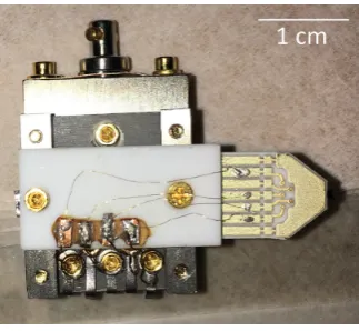
In our first probe design, shown in figures 5 and 6, the Capres probe is epoxied directly to the underside of the
macor base. All of the wiring is 0.002” gold wire, attached to the contact pads with silver paint and routed to copper
contact pads epoxied to the macor. From the macor contact pads, gold wires connect to contact pads on the probe
base which make connection to pins inside the chamber. These pins run to coaxial outputs on the back of the chamber,
which we used to supply voltage and current to the probe. The downside of this design is that the Capres probe may
be slightly tilted in the pitch and roll directions, which can cause the silicon chip to make contact with the sample
before the cantilevers do.
To combat this issue, we redesigned the probe with an adjustable tilt. This newer design is shown in figure 7. The
Capres probe is now attached to a thin piece of macor to provide a non-conductive boundary between it and the bent
steel plate. Three screws pin the steel plate to the probe base, with a small ball bearing in the center. This allows us
to control the tilt angle of the probe by tightening or loosening the screws. The benefit of this design is that we can
adjust the tilt angle easily. This comes at the cost of a height adjustment. There are only about two millimeters of
z-piezo range for the probe, so height adjustments due to the tilt angle need to be countered by adjusting the sample
height, so that the probe will still land on the sample.
FIG. 6: Detailed view of the first generation of four-point probe. The base screws into the ports as shown in figure 5 above. Wiring is 0.002” gold wires held on by silver paint.
FIG. 7: The second generation of four-point probe. a) Image of the probe. The three screws can be tightened or loosened to adjust the tilt angle of the probe, at the cost of a height change. The hole in the top of the steel plate is for a ball bearing. All wiring is insulated copper underneath the steel plate. b) Side view schematic of the probe. The probe base is black, ball bearing and screws are dark gray, bent steel plate is light gray. Off-gold rectangle is the probe itself, with a black chip and yellow cantilevers (magnified for visibility). Copper wires (yellow) come from the bottom of the probe and are fed underneath the steel plate to contact pads on the back of the base.
4. Millimeter-Scale Home-Built Probe
Since the Capres probes are electrostatic discharge sensitive, they are difficult to troubleshoot. To ensure that the
experimental set-up beyond the probe was working (e.g. making sure the cables were connecting properly, that the
electrical feedthrus were making contact with the probe base, etc.), we made a more robust millimeter-scale probe to
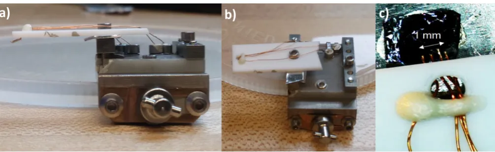
perform the experiments with, shown in figure 8. Modeled after the Capres probe design, our home-built probe has an
outermost cantilever spacing of one millimeter (see figure 8c). These cantilevers are made out of thin insulated copper
in figure 8a, there is no tilt incorporated into the design because the copper wires are easily manipulated by hand.
Bending them with a sharp pair of tweezers allowed us to control the cantilever spacing as well as pitch. However,
since this probe is slightly askew on the yaw axis and a little shorter than the mounted Capres probes, samples have
to be set a few millimeters towards the back right of the sample plate, else the cantilevers will not reach the sample.
FIG. 8: Home-built probe. a) Side view: cantilevers (below macor on the far left) are bent copper wire stripped of insulation that can be positioned by hand with a pair of fine tweezers. b) Top view: wires are fed through a bolt hole in the macor from their connection to the pads on the probe base. c) Cantilevers landed on a black phosphorus crystal, with scale bar.
5. Keithley 2450 SourceMeter
The Keithley 2450 SourceMeter is a current or voltage source and measure device. We used a combination of two
of them to collect data for these experiments. The interactive screen allows users to select the mode of operation
(e.g. source voltage/measure current), change the number of inputs used, or program trigger models. We used these
at first as measure-only devices (sourcing from the battery box, described in section II.A.6), but found that they
function more reliably if they are used as source and measure simultaneously. We wrote programs for data collection
in LabVIEW as discussed in section II.C.2.
6. Battery Box
The battery box is a home-built floating direct current power supply with variable resistors to control the output
voltages and currents. We used this to test our circuit geometry and the magnitude of the resistances before performing
the experiments. Figure 9 is an image of the front of the battery box with its wiring diagram. The battery box can be
operated in positive or negative bias mode based on the ‘+/OFF/-’ switch. The dial is a ten-turn 1kΩ potentiometer.
way, but the control is much finer than for the dial. The resistor selector has seven high-precision resistors so that
if we measure the voltage across I Sense, we know the current over the resistor, which is in series with V Out and
therefore gives us the current over the sample. To take measurements with the battery box, it is best to choose the
resistor on the resistor selector that is closest to the estimated sample resistance. This will keep the voltage measured
over I Sense approximately the same as the voltage over the sample. It is worth noting that if nothing is attached to
V Out, there will never be any voltage over I Sense.
FIG. 9: Circuit diagram and face of the battery box. a) V Out is the output voltage, which has the same current through it as the resistors in the resistor selector. I Sense can then be used to determine what current is being output through V Out. b) Face of the battery box, with labels corresponding to the labels used in the circuit diagram.
B. Measurement Techniques
1. Transport Measurements
We used both two- and four-point measurements extensively in this work to measure sample resistances, as depicted
in figure 10. For two-point measurements (see figure 10a), the voltage and current are measured at the same point,
at the end of the cables in the measurement device. This makes the total circuit resistance equal to R+Rs , where
R is the total resistance of the cables plus the contact resistance, andRsis the sample resistance. Then Ohm’s Law
for the measured voltage isV =I(R+Rs), and the slope of the I-V curve is not the inverse of the sample resistance
alone, but the inverse of the total resistance. This means that all measurements done with the two-point geometry
are inseparable from the condition of the measurement tools and the potential barrier at the contacts. However, since
they are easier to set up than four-point measurements, two-point measurements are an important way to check that
all wires are connected and the probe is landed. If the sample resistance is much greater than the contact and lead
Four-point measurements use a different geometry that removes the I-V curve’s dependence on the lead and contact
resistances (see figure 10b). As with two-point measurements, current is measured in line with the voltage supply, so
I = V
(Rs+R). Unlike two-point measurements, though, the voltage is measured across the sample by a separate pair
of leads connected to a voltmeter. Voltmeters are run in parallel with the circuit element being measured and have a
very high internal resistance, so the voltage drop measured is exclusively due to the sample. In figure 10b, the lead
resistance of the two new cables is added into the voltmeter resistance. The current is unchanged, but the voltage
is measured over the sample itself, so Vmeasured =IRs. By measuring the current and voltage in different locations
(current is measured at points 1 and 4 in figures 10b and 10c; voltage is measured at points 2 and 3), the slope of the
I-V curve is now the inverse of the sample resistance, rather than the inverse of the total resistance. The experiments
described here used four-point measurements exclusively to avoid errors due to contact and lead resistance.
FIG. 10: Two-point and four-point circuit diagrams and illustrative figure of a landed probe. In the diagrams, top resistor is the sample, side resistors are combined lead and contact resistances for the outermost wires and cantilevers of the probe. a) Two-point circuit geometry. Voltage is measured over the entire circuit, so lead resistance is included in the total resistance measurement. b) Four-point circuit geometry. Here, voltage is measured over the sample only, so only sample resistance is measured. c) 30µmfour-point probe landed on a graphite sample to illustrate b). The outer cantilevers represent the resistors on the side in b). The inner cantilevers are the ones measuring the voltage drop and are connected to the voltmeter in the diagram. For a two-point probe, the inner cantilevers do not exist, and current and voltage are both measured between the outer cantilevers. In b) and c), contact points are labeled.
2. Scanning Tunneling Microscopy
Before performing our resistance measurements, we used scanning tunneling microscopy (STM) to examine the
pristine surfaces of the freshly-cleaved samples. STM is a method of imaging the electronic and physical structure of
materials using quantum tunneling of electrons. An atomically-sharp tip (platinum-iridium in our case) controlled by
piezomotors is biased with respect to the sample and scanned over the surface. This bias voltage induces electrons
of states and the topography. Varying the tip-sample bias makes it possible to map out the local density of states
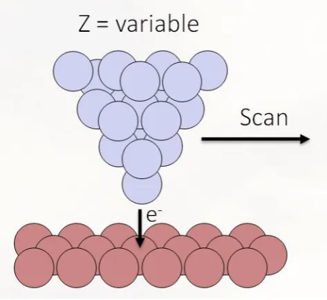
at energies near the Fermi level, which gives the electronic structure of the sample. Figure 11 is a cartoon of the
operation of the STM, showing the tunnel junction. As illustrated, the direction of electron tunneling indicates the
sample is at a higher voltage than the tip.
There are two modes which the STM will scan in: constant current and constant height. Constant current mode
enables a feedback loop so that when the current increases or decreases the z-piezo moves towards or away from the
sample. This allows us to get a semi-topographical image of the sample. If there are features in the sample, like
adatoms or impurities, that have a different local density of states, the feedback loop will register a different current
and the topography map will look as though there is a true height change at that site.
In constant height mode, the tip scans at a set height and plots only the tunneling current at each spot. In this
mode there is no feedback loop to avoid crashing into surface features.
FIG. 11: Diagram of the STM. The tip (blue triangle) is poised above the sample (red surface) with some voltage bias controlled by the STM Rev9 software. The tip will move across the sample picking up a tunneling current at that bias. As it rasters over atoms, the number of electrons picked up by the tip changes based on the height of the atom and the type, so the z-piezo will adjust.
3. Raman Spectroscopy
Phonons, which are vibrational modes in the crystal lattice, can be used as a kind of fingerprint for a material,
since the vibrational modes that are present depend on the structure of the crystal and the type of atom that makes it
purity of a sample. Raman spectroscopy takes advantage of the short-lived excited states for phonons in a solid. We
shine in monochromatic light (here at 532 nanometers), which excites the crystal’s higher energy vibrational states
that quickly decay. The vibrational modes decay by releasing their energy in the form of photons that have the energy
of the difference between the phonon’s excited and ground states. This corresponds to a specific frequency of light.
By measuring the energy of the light, we find the energies of the crystal’s phonon modes. Raman spectroscopy can
also be modeled as an inelastic scattering of photons from a crystal; any energy transferred during scattering surfaces
as a shift in scattered photon energy relative to the incident photon energy. Typically, Raman spectra are shown as
a graph of intensity against Raman shift, which is the change in wavenumber of the emitted light from the incident
light.
For BP, there are typically three prominent peaks shown in the Raman spectrum, plus more for the substrate. The
BP-specific peaks (shown in figure 12) correspond to the A1
g, B2g, and A2g phonon modes at about 361, 438, and 466
cm−1 respectively. According to Favronet al., who took a Raman spectrum every 24 minutes as a BP sample sat in
air, the intensities of each peak decrease after oxidation [16].
FIG. 13: Physical interpretation of the prominent phonon modes in black phosphorus. Adapted from reference [17].
C. Experimental Methods
1. Air-Free Preparation of Samples
Since it is air-sensitive, we store our commercially-bought black phosphorus (from HQ Graphene) in a pure nitrogen
glovebox. For bulk samples, we took small portions off the crystal, cleaved them in the nitrogen environment, and
mounted them to a steel sample plate with conductive epoxy. The epoxy ensures a conductive path from the BP to
the steel, so we can do STM on the sample, and allows us to cleave in vacuum without the sample detaching from the
sample plate. We made flake samples by exfoliation from the bulk using the Scotch tape method inside the nitrogen
glovebox, and we set them on substrates of Si topped with 285nm of SiO2[18].
FIG. 14: This transit chamber helps us keep samples from touching atmosphere when being transferred from the glovebox to our UHV chamber. The end with the gate valve attaches directly to the back of the load lock.
A home-built transit chamber allows us to transport the samples from the glovebox to our ultra-high vacuum
chamber without exposing the samples to air (see figure 14). This transit chamber fits inside the glovebox, so it
load lock on the UHV chamber, which can be brought up to pressure using pure nitrogen and pumped back down to
vacuum once the sample is inside. This method allows us to keep our samples pristine until gases are introduced into
the vacuum chamber.
2. LabVIEW Programs
We primarily used two LabVIEW programs to collect the data and control the Keithley 2450 SourceMeters, which
were our source and measure instruments. The first program is named ‘IV Manual Point Input’, and is used to take
I-V measurements over a range of voltage or current values at a single instance in time. Figure 15 is a screenshot
of the user interface for the program. It can be run in either two-point or four-point mode, which is convenient for
checking the linearity of our I-V measurements. If two-point measurements are non-linear, then the cause usually
turned out to be faulty wiring on the probe. When they are on approximately zero current, then the probes are
making either bad contact or no contact at all. This program allowed us to check that everything was operational
before running the experiments.
FIG. 15: User interface for the IV Manual Point Input program. Shown is a linear curve taken in four-point mode on black phosphorus, indicating the connections were all functioning properly. This is a 100 point sweep from -0.1V to 0.1V, limited at 0.5A.
For continuous four-point measurements, we used the other program, named ‘R vs T-4pt-2 Keithleys GPIB’. This
program takes four-point measurements from one Keithley while taking resistance data from a thermometer on another
Keithley. Since we were not measuring temperature dependence, we did not use this second feature. The output file
for this program is a three column text file with sample resistance, thermometer resistance, and time values for
the first program, though, the Keithleys need to be set up and running before the program is turned on; that is, it is
only a data collection program and does not control the Keithleys itself. To run the Keithleys, they need to be put
into 4-Wire Sense mode in the Measure Settings menu, and set to Source Voltage/Measure Resistance mode under
the Function tab in the Quickset menu. The output voltage and current limit need to be set so that the limit is not
reached and is lower than the damaging current to the probes and sample, which is typically around 1mA (the BP
samples will be damaged if there is a high enough current passed through it, which increases the sample’s resistance).
After all of the configuration, the output button on the top right should be pressed. Only after the Keithley is sourcing
can the program be started, since it will throw out an error if there is nothing to read in yet. When stopping data
collection, the program needs to be stopped before the Keithley output is stopped, or there will again be an error and
the output file will not be produced. In the future, this program should be altered to include set-up control of the
Keithleys and an optional timer to stop measurements after a certain point.
III. RESULTS
A. STM on Black Phosphorus
Before we performed any resistance measurements on the surface of our bulk BP, we imaged the pristine surface of
the crystal with STM (see figure 17). Our STM image shows that after a cleave, there are no foreign atoms on the
material. The dumbbell-shaped defects from phosphorus vacancies are inherent to the crystal [11][12]. These data
confirm the sample surface is free of adsorbates after a cleave. Figure 17 is the STM image we took of bulk BP before
introducing it to gases for the degradation experiment. The ridges in the figure are made of small points–these are
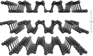
atoms, and the ridges are the structure of the BP crystal, as shown in figure 1.
B. Procedural Outline
We performed four exposure experiments: one at low pressure (5x10⁻⁵ millibar) in air (experiment 1), one at low
pressure in pure O2(experiment 2), one more at low pressure in air (experiment 3), and one at atmospheric pressure
in air (experiment 4). For each of the experiments, the overall procedure was nearly identical: first, we landed the
home-built probe on cleaved bulk BP by using the optical microscope and the procedure outlined in section VIII.A.1.
We checked the connections by doing two-point measurements with a multimeter on the coaxial cables that lead to the
sample. We were only able to use a multimeter because the home-built probe is not electrostatic discharge sensitive;
this could have broken the Capres probes. Using the XY Recorder and battery box in tandem, we checked the
linearity of the two-point measurements. These were then retaken on the Keithleys with the ‘IV Manual Point Input’
program, sweeping voltage from -1mV to +1mV. After all these checks, we began continuous four-point resistance
measurements in vacuum at a constant voltage of +1mV. The exception was experiment 1, when we took four-point
measurements with the battery box approximately every ten minutes.
Once measurements in vacuum had been stable for some time, we leaked gas into the darkened probe chamber.
After hours in this condition, to make sure the gas exposure did not affect the resistance of the sample without the aid
of light, we uncovered the chamber and turned on the halogen microscope bulb from the inverted viewport, diffused
enough that the whole sample was illuminated. This procedure allows us to independently measure whether O2 or
air alone has an effect on BP, and if not, whether light aids the reaction.
C. Exposure Experiments
1. First Low-Pressure Air Exposure Experiment
In this experiment we exposed the sample to low pressures of air, while taking resistance measurements
approxi-mately every ten minutes. Over several measurements in vacuum between -10 and +10 microvolts from the battery
box, we measured the four-point resistance from our sample to be approximately 0.28Ω, a value that did not change
when air was leaked into the chamber at 5x10⁻⁵ millibar. We kept the leak pressure constant for about an hour
and a half, without light. Within three minutes of the sample’s exposure to light from the optical microscope, its
resistance rose to 0.77Ω, nearly a half an ohm higher than pristine measurements. This is shown in figure 18a. All
other measurements, taken over the span of a few hours and again after leaving the light on overnight gave a resistance
kept the leak pressure between 4.2 and 5.1x10⁻⁵ millibar during air tests. Room temperature varied at around 68◦F
and relative humidity stayed at about 30%. This resistance change, if not a real change in the sample (which seems
likely considering the results of the rest of our experiments) could be explained by the fact that we had to put the
optical microscope back on the chamber, which means we had to bump the chamber a little bit. This could have
slightly disturbed the position of the probes.
2. Low-Pressure O2 Exposure Experiment
We began experiment 2 by measuring a steady resistance of 0.60Ω in vacuum. This is a different resistance from
the previous experiment, presumably because the cantilevers had been adjusted between then and this exposure
experiment. As is shown in figure 18b, we still saw no change in the resistance from vacuum conditions, regardless of
the amount of light shone into the chamber. In this case, the amount of light varied because a small ion gauge light
was accidentally left on during the ‘no light’ phase of the experiment. We found an average resistance of 0.662±0.048Ω
for this experiment.
3. Second Low-Pressure Air Exposure Experiment
Experiment 3 began as a continuation of the O2 exposure experiment. We pumped the excess O2 out of the
chamber, without recleaving the sample or moving the probe. We disconnected the O2 tank from the gas manifold
and dosed with 5x10⁻⁵ millibar of air, again at about 30% relative humidity (this time with the ion gauge light off).
We measured over the course of nearly a full day, with light exposure at hour 16. In these conditions, we saw no
change in the sample resistance, with an average of 0.636±0.015Ω.
4. Atmospheric Pressure Air Exposure Experiment
This time we set out to find if there is a critical pressure for which bulk black phosphorus has a change in resistance
on these timescales, since previous attempts only showed null data. Instead of leaking air in at 5x10⁻⁵ millibar,
we exposed the sample to full atmosphere for 14 hours without light, and an additional 9 hours with light. In this
experiment, as can be seen in figure 18d, we initially measured a resistance of about 1.8Ω, much higher than that of
the other experiments. The Keithleys were malfunctioning through the first several hours of the experiment while it
atmosphere exposure. The measurement of 1.8Ω for a four-point resistance agrees with previous measurements on this
sample with this probe before the experiment started, so this much higher resistance is not an instrument error, and is
most likely due to adjusting the cantilever spacing between experiments (discussed further in section IV). Excluding
data from before hour 7, we found an average resistance of 1.779±0.023Ω and no change with air or light exposure.
D. Raman Spectroscopy on Air-Exposed Sample
After full air exposure, we brought the sample to the Raman spectrometer in a sealed container. In reference [16],
the authors note that oxidized black phosphorus does not exhibit any change in the location of the Raman shift peaks,
but does show a decrease in the intensity of these peaks, as shown in figure 12, section II.B.3. Our data shows peaks
located at about 360, 436, and 466 cm−1 before cleaving (which is consistent with the results of previous studies
[16][17][19]) and at the same locations after cleaving, just with much higher intensity. This confirms that the black
phosphorus sample was oxidized from the air exposure, despite the null resistance measurements.
FIG. 19: Raman spectra for our bulk BP sample, with characteristic peaks at 360, 436, and 466 cm−1. Before it was cleaved, it had been left in atmosphere for about a day after air exposure tests. We see an increase in the intensity of the peaks after cleaving (i.e. with a pristine surface) which agrees with the prediction set forth in section II.B.3.
IV. DISCUSSION
A number groups have reported the chemisorption of oxygen molecules into the black phosphorus crystal lattice,
[9][10][13][14]. We did not see the direct impact of degradation on the resistance of our bulk sample. We attribute
this observation to the relative scale of the home-built probe and the thickness of the crystal. By solving Laplace’s
equation for a semi-infinite bulk with constant resistivity everywhere, the four-point resistance of a bulk sample is
found to be
R= 1
2πsσb
(1)
whereσbis the bulk conductivity of the sample, andsis the intercantilever spacing [20]. The surface layers make up a
small fraction of the bulk, so that even though we showed that the surface of the BP sample had oxidized (by Raman
spectroscopy), it is perhaps unsurprising that the four-point resistance did not change, since the bulk conductivity
could not have changed much from surface oxidation. We can use the fact that the resistance is constant to show that
σbdoes not change significantly during exposure, and then estimate the maximum number of layers oxidized in these
experiments.
Because of its buckled structure, black phosphorus has anisotropic resistivity in the plane. As measured by [21]
and [22], at room temperatureρzz ≈1.0 Ωcm, ρac≈0.5 Ωcm, andρil ≈1.0 Ωcm(these are the zig-zag, armchair,
and interlayer resistivities; directions are outlined in figure 1). In a single layer, the resistivity is ρ2 sl =ρ
2
zz+ρ2ac, or
ρsl≈1.1 Ωcm. Sinceρsl is approximately equal toρil, the depth of the current penetration is about the same as the
width the current crosses between cantilevers. With macroscopic cantilevers we can then conclude that nearly all of
the current goes through the bulk, since the penetration depth would have to be nearly the depth of the sample.
By finding the difference in our mean resistances before and after each experiment, which reduces to the uncertainty
in the resistance, we can estimate the maximum number of oxidized layers. Before exposure to gases and light, the
resistance is only dependent on the cantilever spacing and the natural properties of the crystal. After exposure, the
resistance is dependent on the cantilever spacing and the new properties of the crystal. By taking the absolute value
of the difference between the two means, we can directly see only the change in resistance brought on by oxidation
(with uncertainty on this change as the standard deviations of before and after added in quadrature). However, since
there is no significant change in resistance before and after exposure in each experiment, the true difference here is
zero. This means
|Raf ter−Rbef ore|+ p
is the maximum change in resistance due to surface oxidation. We can assume that the total resistivity, given by
ρ2
total=ρ2zz+ρ2ac+ρ2il (soρtotal≈1.5Ωcm) does not change, since only the top few layers are affected by oxidation.
Because resistance is defined by
R=ρ s
wd (3)
(where sis the intercantilever spacing, w is the length of cantilever in contact with the sample, andd is the depth
probed), the change in resistance is
Raf ter−Rbef ore=
ρs wdaf ter
− ρs
wdbef ore
(4)
Equation 4 assumes that any change in resistance is the same as losing probing depth, which is true when the oxidized
layers have a resistivity much greater than the unoxidized layers. Basically, any change in resistance is due to there
being fewer layers the current moves through. This means that, sinceRaf ter−Rbef ore= 0,
√
2∆R≥ ρs
wdaf ter
− ρs
wdbef ore
(5)
If ∆dis the probing depth lost (i.e. the depth of the oxidized layers), thendbef ore−daf ter = ∆d. By combining
this definition with equation 5, the formula for the maximum change in resistance from oxidation is
√
2∆R≥ ρs w
1
dbef ore−∆d
− 1
dbef ore
(6)
We havedbef ore since the probing depth and cantilever spacing are approximately equal for a pristine sample.
There-fore this can be solved for ∆d, the probing depth lost, which when divided by the layer thickness of 5˚A will give the
maximum number of oxidized layers.
Doing this calculation out for all of the experiments withw=0.3mm,s=0.33mm,dbef ore=0.33mm,ρ=1.5Ωcm, and
∆Ras the standard deviation calculated for each experiment and laid out in sections III.C.2-4, the maximum number
of oxidized layers is 900 for the experiment 2, 300 for experiment 3, and 450 for experiment 4. These may be hundreds
The dependence of the four-point resistance on cantilever spacing, as illustrated in equation 1, provides an
ex-planation for the change in measured resistance of the BP flake between the first, middle two, and fourth exposure
experiments. Since the cantilevers on the home-built probe had to be manually adjusted after every few landings, we
can assume that the cantilevers were spaced differently in experiment 1 than they were in experiments 2 and 3 and
in experiment 4, which led to a different resistance for pristine BP each time. Using equation 1, the resistance
mea-surements for pristine BP in experiments 3 and 4, and the assumption that the cantilevers were spaced at 0.33mm in
experiment 3, we can calculate that for the resistance to change from 0.6Ω to 1.8Ω, the inner cantilevers in experiment
4 were spaced at 0.40mm. It is therefore reasonable to assume that bumping the chamber would cause a slight change
in resistance, and adjusting the cantilevers, as had to be done after every few landings, would definitely cause them
to read a different four-point resistance for the same sample.
The type of cantilever spacing dependence of the resistance seen in equation 1,R∝1
s, is not intuitive at first. It is
due to the fact that while the current will take the path of least resistance, there is some spreading out. Approximating
that the spreading of the current is proportional to the shortest distance traveled, we haveR∝ s
wd as in equation 2,
but noww=d=s, leavingR∝1 s [20].
A good follow-up study would be to use the Capres probes on bulk black phosphorus, so that the cantilever spacing
is constant and much smaller than in the experiments we carried out. This would cut down on the number of layers
that the current flows through, so that a higher percentage of them are surface layers, and any change in resistance
due to surface adsorbates would be easier to detect.
A much more interesting experiment would be to repeat these measurements with black phosphorus flakes, which
was the original goal of this study. Flakes are of the thickness that would be used in electronic circuitry, and are
therefore the most useful system to study. BP flakes are usually very small when mechanically exfoliated, so that
only the five micron Capres probes are able to land on these samples.
V. CONCLUSION
In this thesis, I showed the development or explained the operation of all the equipment necessary to take
four-point measurements of bulk black phosphorus in a vacuum chamber, and then showed the results of exposing bulk
BP to atmospheric air and pure oxygen at various pressures. Our results reveal that despite the rapid oxidation of
BP in atmospheric conditions, four-point resistance measurements do not change when either pure O2or atmosphere
interior of the crystal, with comparatively little going through the oxidized layers. We calculate an upper bound on
the number of oxidized layers, with the maximum amount being 900 out of 660,000 total layers probed. In addition
to the work directly on BP, we also built a home-made probe that is robust against electrostatic discharge and can
therefore be used to help troubleshoot our measurement circuits, as well as a tilted design for micron-scale probes to
be used in future experiments.
VI. ACKNOWLEDGMENTS
A research project of this size could not have been undertaken without the help of the rest of the lab and our
collaborators. The glovebox where we store and prepare our samples is located in Dr. Christine Caputo’s laboratory
in the UNH Chemistry Department, and I’d like to thank Jake Riffle for making our samples and Charlie Ayotte
for training Jake and me on glovebox practices. The Raman spectrometer is located in one of Dr. Young Jo Kim’s
laboratories in the UNH Electrical Engineering Department, and I would like to thank Sujoy Ghosh for training me
and Steven Arias on its use. I would also like to thank Steven for helping with the Raman measurements. The time
lapse images of black phosphorus are from a short study done by Patrick Linehan, a former high school intern in the
Hollen lab for the 2016-2017 academic year. For much of the design and work on the second generation of Capres
probes I would like to thank Ben St. Laurent. The STM images and results from our previous study on BP are also
mostly from Jake Riffle, as is the STM schematic (figure 11). I would like to thank all three of the graduate students
(Jake, Ben, and Steven) and our undergraduate, Tan Dao, for helping me take data when things worked and letting
me vent when they did not, in addition to all of their cooperation in scheduling with the microscope, the STM/AFM,
and chamber use in general. I also would of course like to thank my advisor, Dr. Shawna Hollen, for all of the training
she’s given me, from soldering to writing, and for providing me with a direction these last few years.
Lastly, I would like to acknowledge partial funding from the University of New Hampshire’s Center for Advanced
VII. REFERENCES
1. Gusm˜ao, R., Sofer, Z., Pumera, M. “Black Phosphorus Rediscovered: From Bulk Material to Monolayers”. Angew. Chem. Int. Ed. 56(28), 2017.
2. Bridgman, P. “Two New Modifications of Phosphorus”. J. Am. Chem. Soc. 36(7), 1914.
3. Andrei, E., Li, G., Du, X. “Electronic Properties of Graphene: A Perspective From Scanning Tunneling Mi-croscopy and Magnetotransport”. Rep. Prog. Phys. 75(5), 2012.
4. Radisavljevic, B., Radenovic, A., Brivio, J., Giacometti, V., Kis, A. “Single-Layer MoS2 Transistors”. Nat. Nanotechnol. 6(1), 2011.
5. Qiao, J., Kong, X., Hu, Z., Yang, F., Ji, W. “High-Mobility Transport Anisotropy and Linear Dichroism in Few-Layer Black Phosphorus”. Nat. Commun. 5, 2014.
6. Morita, A. “Semiconducting Black Phosphorus”. Appl. Phys. A 39(4), 1986.
7. Zhu, W., Yogeesh, M., Yang, S., Aldave, S., Kim, J., Sonde, S., Tao, L., Lu, N., Akinwande, D. “Flexible Black Phosphorus Ambipolar Transistors, Circuits and AM Demodulator”. Nano Lett. 15(3), 2015.
8. Churchill, H., Jarillo-Herrero, P. “Two-Dimensional Crystals: Phosphorus Joins the Family”. Nat. Nanotechnol. 9(5), 2014.
9. Ziletti, A., Carvalho, A., Campbell, D., Coker, D., Castro Neto, A. “Oxygen Defects in Phosphorene”. Phys. Rev. Lett. 114(4), 2015.
10. Utt, K., Rivero, P., Mehboudi, M., Harriss, E., Borunda, M., San Juan, A., Barraza-Lopez, S. “Intrinsic Defects, Fluctuations of the Local Shape, and the Photo-Oxidation of Black Phosphorus”. ACS Cent. Sci. 1(6), 2015.
11. Riffle, J., Flynn, C., St. Laurent, B., Ayotte, C., Caputo, C., Hollen, S. “Impact of Vacancies on Electronic Properties of Black Phosphorus Probed by STM”. J. Appl. Phys. 123(4), 2018.
12. Kiraly, B., Hauptmann, N., Rudenko, A., Katsnelson, M., Khajetoorians, A. “Probing Single Vacancies in Black Phosphorus at the Atomic Level”. Nano Lett. 17(6), 2017.
13. Huang, Y., Qiao, J., He, K., Bliznakov, S., Sutter, E., Chen, X., Luo, D., Meng, F., Su, D., Decker, J., Ji, W., Ruoff, R., Sutter, P. “Interactions of Black Phosphorus with Oxygen and Water”. Chem. Mater. 28(22), 2016.
14. Hu, Z., Li, Q., Lei, B., Zhou, Q., Xiang, D., Lyu, Z., Hu, F., Wang, J., Ren, Y., Guo, R., Goki, E., Wang, L., Han, C., Wang, J., Chen, W. “Water-Catalyzed Oxidation of Few-Layer Black Phosphorus in a Dark Environment”. Angew. Chem. Int. Ed. 56(31), 2017.
15. Petersen, C., Hansen, T., Bøggild, P., Boisen, A., Hansen, O., Hassenkam, T., Grey, F. “Scanning Microscopic Four-Point Conductivity Probes”. Sens. Actuators A Phys. 96(1), 2002.
16. Favron, A., Gaufr`es, E., Fossard, F., Phaneuf-L’Heureux, A., Tang, N., L´evesque, P., Loiseau, A., Leonelli, R., Francœur, S., Martel, R. “Photooxidation and Quantum Confinement Effects in Exfoliated Black Phosphorus”. Nat. Mater. 14(8), 2015.
17. Sugai, S., Shirotani, I. “Raman and Infrared Spectroscopy in Black Phosphorus”. Solid State Commun. 53(9), 1985.
18. Novoselov, K., Geim, A., Morozov, S., Jiang, D., Zhang, Y., Dubonos, S., Grigorieva, I., Firsov, A. “Electric Field Effect in Atomically Thin Carbon Films”. Science 306, 2004.
19. Ribeiro, H., Pimenta, M., de Matos, C. “Raman Spectroscopy in Black Phosphorus”. J. Raman Spectrosc. 49(1), 2018.
20. Wells, J. “A Combined Study of the Electronic Structure and Transport Properties of Surfaces”. Doctoral Thesis, University of New Hampshire, University of Aarhus. 2006.
21. Akahama, Y., Endo, S., Narita, S. “Electrical Properties of Black Phosphorus Single Crystals”. J. Phys. Soc. Jpn. 52(6), 1983.
VIII. APPENDICES
A. Procedural Appendix
1. Landing the Probes
With the probes mounted onto bases that attach to the piezomotor-controlled stage inside the probe chamber and
an optical microscope to look in with, gentle landings are possible. With the home-built probe, the voltages on the
approach and retract settings can be set to 150 volts each, because the copper wire is forgiving enough that it only
permanently bends slightly for every hard landing, and the probes can be manually realigned if necessary.
However, with the Capres probes, we needed to use a different technique, since the cantilevers are fairly brittle. To
land these, we positioned the probe in the approximate x- and y-coordinate that we wanted (by viewing the sample
in the microscope and moving the probe around until we saw a shadow above the sample) and then focused the
microscope slightly above the sample. We used a larger voltage to approach (usually either 120 or 150 volts) until
the cantilevers were almost in focus in the microscope. We then cut down the voltage to about 80 volts and changed
the step setting to 10 steps per click. With repeated clicks the cantilevers would come into focus, at which point we
refocused the microscope on the sample and repeated the same process, eventually cutting down to 5 steps per click
and then 3 steps per click when we got very close to the surface.
One indicator of contact is a slight discoloration of the tips of the cantilevers; they become darker on the ends.
Another indicator (which only works if the circuit is known to be functioning properly) is to make a two-point
measurement between any two cantilevers with a very small constant voltage applied from the battery box, with the
X-Y Recorder as the measurement apparatus. When the cantilevers touch the sample, the tracer on the X-Y Recorder
will visibly and audibly jump.
2. Testing the Capres Probes
One good way to test that the probe is operational is to land it on a conductive sample. Capres recommends
ruthenium wafers specifically, although we seem to be able to work well with exfoliated graphite samples. However,
gold samples are to be avoided, because landing the gold-coated cantilevers on the gold samples and running a
current through appears to encourage a type of electroplating, which leaves the cantilevers bare of gold and thus
3. Approach and Retract Piezo Settings
Typical voltages for approach and retract were between 120 volts and 150 volts. These settings are found in the
‘RHK PMC 100’ box on the Rev9 software, after clicking the ‘Config Settings’ button. Motor 2 is the probe station
control (Motor 1 is the STM/AFM and Motor 3 is unwired). On the hand-held Rev9 remote, the sliding motor
indicator works in the same way; i.e. Motor 2 is the one being moved when the indicator is at 2. However, the
directions on the remote are dependent on whether Rev9 is opened in STM or AFM mode. In STM mode, up and
down on the remote are retract and approach, respectively, but in the configuration settings menu, ‘Approach’ is
retract and ‘Retract’ is approach. In AFM mode, up and down on the remote are reversed (i.e. up is approach), while
the controls are as labeled in the configuration settings menu.
B. Previous Work
Reference [11] is an article published in the Journal of Applied Physics by the members in our lab, including me.
In that study, we looked at the inherent dumbbell-shaped defects in the crystal, which p-dope the material as a
whole. We compare defect-densities of two commercially available types of black phosphorus, from HQ Graphene (the
same as was used in these experiments) and from 2D Semiconductors. We used STM and STS (Scanning Tunneling
Spectroscopy) to characterize these defects, and show that air-induced defects play a much bigger role in changing
transport properties than the intrinsic defects do. In doing this research, we figured out many of the physical difficulties
of black phosphorus, which included designing the transit chamber to get samples from the chemistry building to the
physics building and learning how to control dose pressure. Much of the black phosphorus handling skills came from