University of Pennsylvania
ScholarlyCommons
Publicly Accessible Penn Dissertations
1-1-2012
Semiconductor Nanowires: Optical Properties and
All-Optical Switching
Brian Edward Piccione
University of Pennsylvania, [email protected]
Follow this and additional works at:http://repository.upenn.edu/edissertations
Part of theMechanics of Materials Commons,Nanoscience and Nanotechnology Commons, and theOptics Commons
This paper is posted at ScholarlyCommons.http://repository.upenn.edu/edissertations/560
For more information, please [email protected]. Recommended Citation
Piccione, Brian Edward, "Semiconductor Nanowires: Optical Properties and All-Optical Switching" (2012).Publicly Accessible Penn Dissertations. 560.
Semiconductor Nanowires: Optical Properties and All-Optical Switching
Abstract
The optical properties of semiconductor nanowires are both important from a fundamental materials physics standpoint and necessary to understand in engineering applications: nanowire photovoltaic devices, sensors, and lasers, among others, could all benefit. Unfortunately, these optical properties are not easy to ascertain. Transmission times are short, in-coupling of white probe light is difficult, and the angle-resolved
measurements typically used to determine material dispersion relations in bulk materials are hindered by diffraction effects at subwavelength nanowire end facets.
Here, we present a series of experimental techniques and theoretical models developed to study of the optical properties of active nanowire waveguides. Beginning with a technique for determining the waveguide dispersion of individual ZnSe nanowires, we demonstrate enhanced properties with respect to bulk material. After investigating propagation loss in individual CdS nanowires, the theoretical model was then refined to quantify the strength of light-matter coupling, where size-dependence was observed. The knowledge gained from these studies was put to use in the first demonstration of all-optical switching in individual
semiconductor nanowires. The switch concept was then extended into an all-optical nanowire NAND gate. These developments highlight the importance of semiconductor nanowires as both model materials systems and novel devices.
Degree Type Dissertation
Degree Name
Doctor of Philosophy (PhD)
Graduate Group
Materials Science & Engineering
First Advisor Ritesh Agarwal
Keywords
CdS, Materials, Nanophotonics, Nanowires, Optics, Polaritons
Subject Categories
Mechanics of Materials | Nanoscience and Nanotechnology | Optics
SEMICONDUCTOR NANOWIRES:
OPTICAL PROPERTIES AND ALL-OPTICAL SWITCHING
Brian Piccione
A DISSERTATION
in
Materials Science and Engineering
Presented to the Faculties of the University of Pennsylvania
in
Partial Fulfillment of the Requirements for the
Degree of Doctor of Philosophy
2012
Supervisor of Dissertation
Signature ______________________
Ritesh Agarwal, Associate Professor, Materials Science and Engineering
Graduate Group Chairperson
Signature ______________________
Russell Composto, Associate Professor, Materials Science and Engineering
Dissertation Committee
Dawn Bonnell, Trustees Chair Professor, Materials Science and Engineering
Ertugrul Cubukcu, Assistant Professor, Materials Science and Engineering
SEMICONDUCTOR NANOWIRES: OPTICAL PROPERTIES AND ALL-OPTICAL
SWITCHING
COPYRIGHT
2012
iii ACKNOWLEDGEMENT
I would like to acknowledge all the support I’ve received for the past five years. My
father Ed, my mother Michele, and my brothers Matt and Ed have always been there for
support. Christine Fox was an inspiration and gave me the strength to keep going. In no
particular order, I’d like to thank everyone else who’s helped me along the way: Rose
Mutiso and Mike Deaven, Mark and Mindy Licurse, Dave Kim and Jenica Abram,
Kristen Metkus, Kate Murphy, Lisa Chen, Anindita Basu, Matt Caporizzo, Dagny
Fleischman, Pat Overend, Profs. Russ Composto, Peter Davies, Cherie Kagan, and John
Blendell, Bart and Lauren Burgess, Mike Burke, Nick Luciano, Alexandria and Aaron
Coble, Kasey and Jill Soska, Mike Willis, Rob Huber, Ryan and Karisa Greecher, Sarah
Selzer and Jason Pfleiger, Kate Hoch, Michael Kovach, Jason Lally, Abigail Fox,
Heather Hurst, Jasmine Malik, Nicole Marotta, Jenn DeLuca, David Ewoldt, Nikki
Cooper, and Matt Stanford.
I’d like to thank my dissertation committee: Profs. Dawn Bonnell, Ertugrul Cubukcu, and
Arjun Yodh. My adviser, Prof. Ritesh Agarwal, has made all of this possible, and I will
always be grateful for his guidance. From the Agarwal group: Drs. Lambert K van Vugt,
Chang-Hee Cho, Yeonwoong Jung, and Chris Rodd, Aaron Wirshba, Carlos Aspetti,
Joohee Park, Pavan Nukala, Rahul Agarwal, Siddharth Ghosh, Karthik Kumar, Tyler
Zimmerman, Thomas Walsh, and Andrew Jennings.
Finally, I would like to thank Kate Huber and Temple University for saving me countless
iv ABSTRACT
SEMICONDUCTOR NANOWIRES:
OPTICAL PROPERTIES AND ALL-OPTICAL SWITCHING
Brian Piccione
Ritesh Agarwal
The optical properties of semiconductor nanowires are both important from a
fundamental materials physics standpoint and necessary to understand in engineering
applications: nanowire photovoltaic devices, sensors, and lasers, among others, could all
benefit. Unfortunately, these optical properties are not easy to ascertain. Transmission
times are short, in-coupling of white probe light is difficult, and the angle-resolved
measurements typically used to determine material dispersion relations in bulk materials
are hindered by diffraction effects at subwavelength nanowire end facets.
Here, we present a series of experimental techniques and theoretical models developed to
study of the optical properties of active nanowire waveguides. Beginning with a
technique for determining the waveguide dispersion of individual ZnSe nanowires, we
demonstrate enhanced properties with respect to bulk material. After investigating
propagation loss in individual CdS nanowires, the theoretical model was then refined to
quantify the strength of light-matter coupling, where size-dependence was observed. The
all-v optical switching in individual semiconductor nanowires. The switch concept was then
extended into an all-optical nanowire NAND gate. These developments highlight the
importance of semiconductor nanowires as both model materials systems and novel
vi TABLE OF CONTENTS
Chapter 1. Introduction ... 1
1.1. Semiconductor nanowires ... 1
1.2. Optical properties of optically active semiconductor nanowires ... 4
1.3. All-optical switching in semiconductor nanowires ... 7
Chapter 2. Nanowire Growth and Experimental Methods ... 18
Chapter 3. Size-Dependent Waveguide Dispersion in Nanowire Optical Cavities ... 24
3.1. Experimental procedures ... 25
3.2. Numerical calculations... 29
3.3. Discussion ... 30
Chapter 4. Propagation Loss Spectroscopy on Single Nanowire Active Waveguides . 40 4.1. Experimental procedures ... 41
4.2. Discussion ... 47
Chapter 5. Variable Temperature Spectroscopy of As-Grown and Passivated CdS Nanowire Waveguide Cavities ... 58
5.1. Experimental methods ... 60
5.2. Results and discussion ... 60
Chapter 6. Incorporating Polaritonic Effects in Semiconductor Nanowire Waveguide Dispersion ………..81
Chapter 7. One-Dimensional Polaritons With Size-Tunable and Enhanced Coupling Strengths in Semiconductor Nanowires ... 91
7.1. Materials and methods ... 93
7.2. Experimental results... 93
7.3. Numerical mode volume calculations ... 97
7.4. Analysis of enhanced oscillator strengths ... 100
Chapter 8. All-Optical Active Switching in Individual Semiconductor Nanowires .. 109
8.1. Experimental setup... 110
vii 8.3. Analysis of switching mechanisms ... 115
Chapter 9. Future Work ... 127
viii LIST OF TABLES
ix LIST OF ILLUSTRATIONS
Figure 1.1: Schematic of the vapor-liquid-solid (VLS) growth mechanism. ... 3
Figure 1.2: Field intensity distribution for the fundamental waveguide mode inside
glass-rod-in-air photonic nanowires for various sub-micron core radii and a wavelength of 800
nm. ... 10
Figure 2.1: SEM image of CdS nanowires as grown and TEM image of single nanowire
transferred onto a carbon lace sample grid. ... 19
Figure 2.2: Micro-photoluminescence setup used in most optical measurements. ... 21
Figure 3.1: a) Scanning electron microscopy image of a ZnSe nanowire dispersed onto a
300nm thick SiO2 covered Si wafer. ... 27
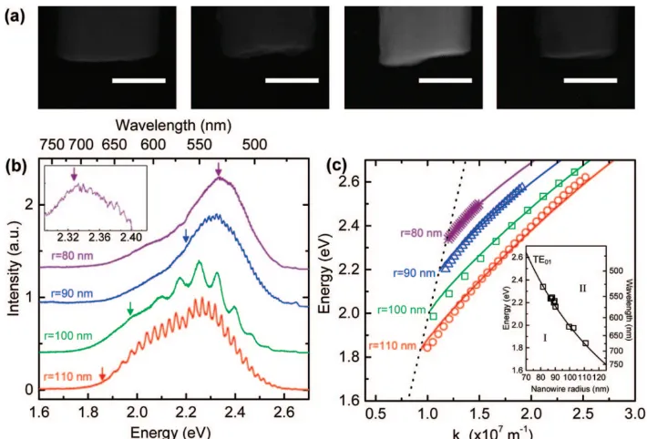
Figure 3.2: a) SEM images of four ZnSe nanowires having radii of 110, 100, 90 and 80
nm and lengths of 5.98, 2.08, 11.51 and 22.28 µm respectively (left to right). Scale bars are 100 nm... 32
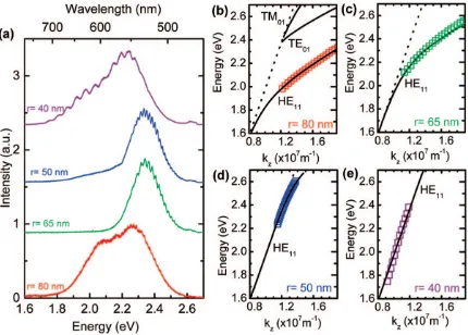
Figure 3.3: Emission spectra acquired from the ends of nanowires with radii of 75, 65, 50
and 40 nm and lengths of 8.52, 8.02, 33.15 and 14.01µm respectively, with increasing
diameters from top to bottom trace, and dispersion of the HE11mode of the nanowires
with radii of 75 nm, 65 nm, 50 nm, and 40 nm, respectively. ... 34
Figure 3.4: Emission spectrum acquired from the end of a nanowire, mode dispersion,
x Figure 4.1: Scanning electron microscopy images of three CdS nanowires dispersed onto
a 300 nm thick SiO2-covered Si wafer on which optical measurements were performed,
and real color optical image of a CdS nanowire under focused 458 nm Ar+ laser
illumination. ... 43
Figure 4.2: Illustration of CdS nanowireunder focused 458nm Ar+ laser excitation at 300
K, spatially resolved excitation images obtained at energies 2.304 and 2.440 eV, and
normalized intensity vs. distance of the excitation laser from the end facet line profiles
extracted from the spatially resolved images. ... 45
Figure 4.3: Propagation loss spectrum at 300 K, plotted alongside photoluminescence
from nanowire end facets ... 47
Figure 4.4: Propagation loss spectrum at a cryostat-reported temperature of 77.6 K,
obtained by plotting propagation loss coefficient as a function of energy. A waveguided
photoluminescence spectrum from the same nanowire, exhibiting longitudinal
Fabry-Pérot resonances, is also shown. ... 49
Figure 4.5: Propagation loss spectra at 77.6 K, ordered according to propagation loss
coefficient at 2.525 eV. ... 52
Figure 4.6: Photoluminescence and dispersion for a nanowire at a cryostat-reported
temperature of 77.6 K. ... 54
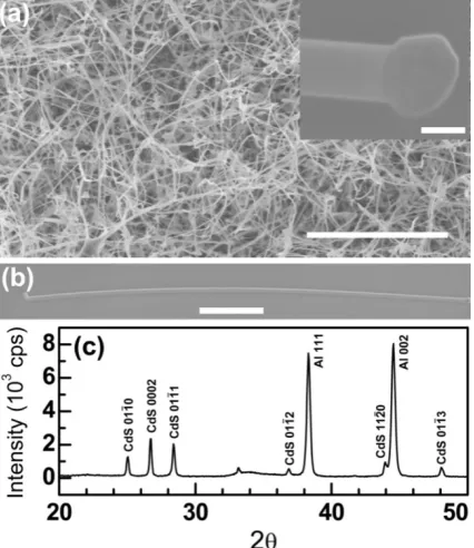
Figure 5.1: SEM image of the nanowire growth substrate, SEM image of an individual
nanowire, on the optical measurement substrate, and an x-ray diffractogram of a CdS
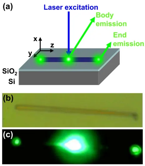
xi Figure 5.2: Spatially resolved optical measurement geometry, reflected white light
microscopy image of a single CdS nanowire, and photoluminescence image of a
nanowire ... 64
Figure 5.3: Room temperature photoluminescence spectra of body emission and end
emissionof an unpassivated CdS nanowire, and 77.6 K photoluminescence spectra of
body emission and end emission... 66
Figure 5.4: Photoluminescence spectra of body and end emission of an unpassivated CdS
wire over the 77.6 K to 298 K temperature range. ... 68
Figure 5.5: TEM image of a 5 nm SiO2 ALD coated CdS nanowire, and fourier transform
infrared absorption (FTIR) spectrum of an ensemble of SiO2 passivated (blue line) and
unpassivated (black line) CdS nanowires. ... 70
Figure 5.6: Room temperature photoluminescence spectra of body emission and end
emission of an unpassivated CdS nanowire, and 77.6 K photoluminescence spectra of
body emission and end emission... 72
Figure 5.7: Photoluminescence spectra of body and end emissions of a SiO2 coated CdS
wire over the 77.6 K to 298 K temperature range, and temperature dependence of the
observed photoluminescence peaks ... 74
Figure 5.8: Photoluminescence spectra of body and end emissions of a SiO2 coated CdS
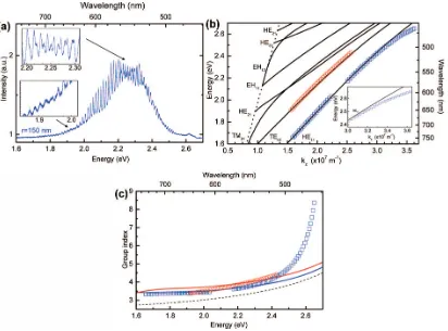
xii Figure 6.1: Waveguide dispersion for the waveguide modes of a CdS nanowire with a
radius of 120 nm calculated using a Sellmeier equation for material dispersion and the
polaritonic model ... 84
Figure 6.2: Emission spectra of guided photoluminescence light for multiple nanowires.
... 87
Figure 6.3: Group index vs. energy for purely photonic and polaritonic modes of two
nanowires ... 88
Figure 7.1: CdS nanowire waveguide cavity and low-temperature spatially-resolved
micro-photoluminescence experimental geometry ... 95
Figure 7.2: Photoluminescence spectra of the guided emission and size-dependent
light-matter coupling strength. ... 96
Figure 7.3: Numerical mode volume calculations of CdS nanowire waveguide cavities.
... 99
Figure 7.4: The transition from the bulk-polariton to the confined cavity-polariton
regime. ... 102
Figure 7.5: n×f for nanowires in the constant coupling strength regime plotted against real
nanowire volume V. ... 104
xiii Figure 8.2: PL spectrum collected from nanowire end facet at 4.1 K showing laser
emission at 2.527 eV, consistent with known literature values for exciton-exciton lasing
in CdS nanowires.. ... 112
Figure 8.3: All optical active switching in CdS nanowires ... 114
Figure 8.4: Photoluminescence collected from the center of a passivated CdS nanowire held at 77K under different applied pump powers ... 116
Figure 8.5: Photoluminescence spectra collected from bottommost facet of a nanowire illustrating the determination of the switching mechanism ... 118
Figure 8.6: Mechanism of switching phenomena in CdS nanowires. ... 121
Figure 8.7: All optical nanowire NAND gate. ... 123
Figure 9.1: Illustration of scanning detection experiment setup. ... 129
1 MAIN TEXT
Chapter 1. Introduction
Portions in preparation for submission to Philosophical Magazine.
1.1.Semiconductor nanowires
Semiconductor nanowires, one-dimensional semiconductor structures with
nanometer-scale dimensions, have received significant attention in the last decade.1 First
synthesized by Wagner and Ellis in 1964,2 the novel nanostructures have since been
proposed as active components, and interconnects, in a multitude of nanoscale devices:
biosensors,3, 4 gas sensors,5-7 nanogenerators,8, 9 light-emitting diodes,10, 11
electrically-driven lasers,12 solar cells,13 and complete programmable circuits14 have all been
demonstrated. Benefits gained from high-surface-to-volume ratios, as well as electrical
or optical confinement in the radial direction, are easily accessible via connections to
nanowire long axes, making nanowires the ideal morphology for many of these
applications. While nanowire synthesis cannot yet produce large-scale integrated
systems as complex as those possible via “top-down” fabrication methods, where bulk
material is reduced in size to desired dimensions, the “bottom-up” methods utilized in
nanowire synthesis, which rely on self-assembly of molecular components by principles
of molecular recognition, typically result in high yields with consistent physical
properties and comparatively superior surface conditions.15
Among the most common synthesis methods, solution growth offers the potential
for high-volume synthesis at near-ambient environmental conditions,16 but low
2 substrates currently limit its utility in integrated device applications. Electrochemical
deposition in combination with nanoporous templates (e.g., anodic aluminum oxide) can
produce much higher aspect ratios at comparably inexpensive environmental
conditions;17 however, the crystals which result are typically either amorphous or
polycrystalline in nature, somewhat limiting their potential in electronic applications and
severely hindering their utility in optical applications. When semiconductor nanowires
possessing both high aspect ratios and crystalline quality are desired, the most reliable
method is currently the same as that first used by Wagner and Ellis, known as the
vapor-liquid-solid (VLS) process.
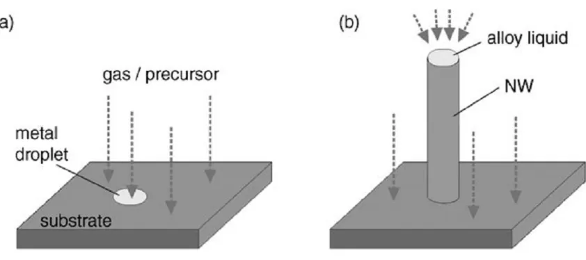
As shown in Figure 1.1, the VLS mechanism can be described as a two-step
proccess.18 After small metal clusters are deposited on the desired growth substrate, the
assembly is placed in a reaction tube and heated until the clusters melt: frequently
achieved by the metal forming an alloy with the substrate, with a reduced melting point
compared to the pure metal. A gas containing the semiconductor growth material is then
introduced to the reaction tube and begins to saturate the liquid alloy. When this alloy
reaches the point of supersaturation, the semiconductor component is expelled at the
liquid/substrate interface, resulting in vertical growth of the desired semiconductor
nanowire crystal. Nanowire composition, morphology, and orientation can all be
controlled through variations on the basic technique: superlattice structures can be
produced by alternating the vapor phase reactants,19 core/shell structures can be produced
by altering vapor phase pressure to induce radial growth,20 and substrate lattice matching
3 deposited determines final nanowire diameters, and controlled placement22 can be used to
create ordered arrays.
Figure 1.1: Schematic of the vapor-liquid-solid (VLS) growth mechanism. a) A substrate
coated with metal clusters is heated until the metal melts, and gas containing the desired nanowire material is introduced to the growth chamber. b) Upon supersaturation, the droplet expels material at the substrate surface, resulting in vertical nanowire growth.18
Control over physical properties of nanowires during growth subsequently allows
for control over properties: among many others, electrical,23 magnetic,24 thermal,25 and
mechanical26 properties are all altered in the nanowire form. Most relevant to this
dissertation, however, are the optical properties of nanowires. Section 1.2 discusses these
properties in more detail, while Section 1.3 details a novel exploitation of the enhanced
4 1.2.Optical properties of optically active semiconductor nanowires
In regards to optical properties, self-assembled, single-crystalline nanowires
occupy an important niche among nanostructure morphologies. Due to a high refractive
index mismatch with their surroundings, semiconductor nanowires with diameters in the
subwavelength regime can strongly confine optical waves in the radial direction while
guiding light in the axial direction,27, 28 a unique combination which makes them ideally
suited for the development of many nanophotonic systems including modulators,29
switches,30 probes,31 and sensors.32 Achieving the full potential of nanowire systems,
however, requires a fundamental understanding of how properties vary as a function of
size, and the size dependence of nanowire optical phenomena was, until recently, poorly
covered in the literature. While photoluminescence,33 optically-pumped lasing,34, 35
waveguiding,36 and photoconductivity,37 for example, have been extensively documented
in individual nanowires, explicit studies of these phenomena and their underlying
physical causes as a function of size have only recently reached sufficient volume for
critical meta-analysis. Massively parallel synthesis methods38, 39 resulting in large
quantities of nanowires per batch allow for a higher probability of obtaining a single
suitable crystal demonstrating a novel phenomenon, but systematic study as a function of
size has significantly more stringent requirements. In addition to controlled synthesis of
consistently high-quality, single-crystalline nanostructures of narrow size distribution,
optical studies of individual nanowires have an additional barrier towards actuation in
that their diameters are typically smaller than the wavelengths of light utilized in far-field
5 The resulting diffraction limitations in this one dimension certainly do not
preclude study of all optical properties, and indeed, the earliest studies of optical
properties (e.g. effects of quantum confinement40 and non-radiative surface
recombination41 on luminescence) were not hindered by this issue. However, a
comprehensive, quantitative analysis of light-matter interaction within any condensed
matter system requires knowledge of the full energy-wavevector dispersion relation, and
it measurement of this which is made difficult by the nanowire geometry. Direct
measurements are commonly performed by angle-resolved transmission or emission
experiments42, 43 and time-resolved transmission experiments can measure its derivative,
the group velocity.44 For nanowires these measurements are hindered by the scrambling
effect of the subwavelength apertures at the wire ends due to diffraction,45 the short
transmission times involved46 and the difficulty of in-coupling of probe light with a large
energy and wavevector distribution.47
The complete energy-wavevector dispersion relation is ultimately defined by both
the nanowire geometry and the materials system, and in the case of active optical
materials, resonant coupling between the light field and the material considerably
complicates waveguide behavior in comparison with passive waveguides. It is known
that due to the substantially larger oscillator strength of electron-hole pairs (excitons)
than that of free electron and hole (band to band) recombination, excitons can strongly
couple to the light field resulting in the formation of composite quasiparticles with both
electronic and photonic character known as exciton-polaritons.48 Energy oscillates back
and forth between the excitonic and photonic states with what is known as the Rabi
6 polariton branches (UPB and LPB) in the material dispersion relation, and drastic
changes to the dielectric function. It is through this polaritonic coupling mechanism, as
well as effects such as giant exciton oscillator strength and superradiance effects,49, 50 that
finite crystal sizes comparable to the optical wavelengths can result in material dispersion
that is significantly different from that of macroscopic crystals.51
Among materials which exhibit polaritonic effects, popular choices for active
nanowire waveguides include ZnO, ZnSe, CdS, GaN, and SnO2, all semiconductors
exhibiting a relatively high refractive index, a direct electronic bandgap, and the
formation of excitons as dictated by their relatively large exciton binding energies.52
Nanowires of two different semiconducting materials were synthesized for the purposes
of this dissertation. The material used in Chapter 3 is zinc selenide (ZnSe), a direct
bandgap II-VI semiconductor which has been employed in both light-emitting53, 54 and
detecting55 configurations, as well as transmissive optical components due to its generally
low absorption coefficient in the infrared.56 The following chapters, however, focus on
cadmium sulfide (CdS), another direct bandgap II-VI semiconductor which has been
extensively studied in bulk57-60 where it has been established that in its wurtzite crystal
structure, the crystal field and spin-orbit coupling61-63 cause the valence band to split into
three levels, giving rise to A, B, and C excitons. Due to a high exciton binding energy of
27 meV64 and high oscillator strengths of 1.84 and 1.35 meV for the A and B excitons,
respectively,65, 66 these excitons can couple strongly to the optical field, significantly
altering the dielectric function and waveguide dispersion of the material.67 Signatures of
exciton-polaritons such as strong dispersion,68 reduced group velocity69 and increased
7 Though the groundwork for obtaining complete dispersion relations from
individual nanowires was first laid by van Vugt et al.71 using ZnO,72 and the resulting
experimental waveguide dispersion relation was also found to be substantially modified
from bulk material, the size-dependence data and analysis tools necessary to draw
quantitative conclusions regarding the strength of light-matter enhancement in the
nanowire morphology were not yet available before the work presented in this
dissertation. Following a brief overview of our experimental setup in Chapter 2, Chapter
3 presents the first use of the analytical tools developed by van Vugt to obtain
size-dependent data from ZnSe nanowires. Chapter 4, details a method for obtaining
propagation losses in individual nanowires, Chapter 5 discusses a surface passivation
method which led to improved optical properties, and Chapter 6 details refinements to the
theoretical waveguide model which allows for quantification of light-matter coupling
strength enhancement. In Chapter 7, all previous developments are combined for a
quantitative size-dependent study of light-matter coupling in CdS nanowires,
unambiguously showing the transition from bulk- to cavity-polaritons for the first time.
1.3.All-optical switching in semiconductor nanowires
The condition in which two different output intensities are possible for a given
optical input intensity, traditionally defined as optical bistability,73, 74 was first described
theoretically and observed experimentally using an absorptive optical nonlinearity by
Szoke et al in 1969.75 Though the condition can manifest in vapors76 and soft matter,77
optical bistability in semiconductors78 in particular was the subject of intense interest in
8 solid-state optically bistable elements.79 Though digital optical computers offer the
potential advantage of very short switching times and massive parallelism in data
processing,80 interest in their development gradually faded due in part to the elements’
power disadvantages when compared with their all-electronic counterparts.81 The power
requirements of these early devices were not symptomatic of optical bistability itself,
rather, they were a consequence of the necessity for strong optical nonlinearity, which
itself benefits from high optical intensities. When combined with suitable feedback, this
nonlinearity will give rise to a static hysteresis loop in the relation between incident and
transmitted (or reflected) light intensities characteristic of optically bistable systems.
More recently, computing applications of photonics have regained relevance.
Imminent bandwidth limitations of electronic integrated circuits82 is stimulating intense
activity in the area of nanophotonics for the development of on-chip optical components,
and solutions incorporating direct bandgap semiconductors are important to this end.83
The exciting prospects of optical processing84 and interconnects85 require a large toolbox
of high-performance components that includes emitters, detectors, modulators,
waveguides and switches. Semiconductor nanowires with superior surface properties86
and strong optical confinement in comparison to components fabricated via top-down
methods can serve as both candidates for nanowire-based optical networks,87 as well as
model systems for furthering the understanding of optical processes in confined
structures.88
As mentioned earlier, high power requirements are not an inherent flaw of
optically bistable systems, rather, the high optical intensities necessary to bring about
9 Additionally, achieving these high intensities in bulk materials requires tight focusing,
which leads to a shortened light-matter interaction length due to the reduced confocal
parameter.89 Attempts to circumvent these issues thus far have resulted in various
integrated solutions, including vertical-cavity optical amplifiers90 and ring resonators,91
all of which show promise but can exhibit an unnecessarily large footprint. Various
hybrid electro-optic switches92-94 and even electro-optic nanowire modulators95 have been
realized, but these devices cannot fully exploit the speed advantages offered by all-optical
counterparts and would be incompatible with an all-optical circuit architecture.
Within the realm of all-optical devices, the nanowire waveguide geometry is an
ideal structure for minimizing the input power needed to induce bistability since it both
maximizes light confinement in the radial direction and provides an effective light-matter
interaction length as long as the nanowire itself. Though dielectric contrast between the
waveguide core (refractive index ncore) and its cladding (refractive index nclad) ceases to
tightly confine light beneath a certain critical radius rc where evanescent fields begin to
dominate, as shown in Figure 1.1, even the modest contrast between a glass rod
(ncore=1.42) and air (nclad=1) provides maximal fundamental waveguide mode light
intensity for radii well below a micron. The empirical relationship for rc (Equation 1.1)96,
97
makes explicit that for a given vacuum wavelength λ the critical radius is inversely
proportional to the quantity ncore-nclad: simply increasing the core refractive index to
10
Figure 1.2: Field intensity distribution for the fundamental waveguide mode inside
glass-rod-in-air photonic nanowires for various sub-micron core radii and a wavelength of 800 nm. The field confinement increases as the core is reduced until a point where
the evanescent field dominates. This critical radius at which maximal intensity is reached decreases as dielectric contrast between the core and its cladding is increased.89
8 . 0 2 . 1 2 ) ( ) ( 573 . 0 clad core clad core c n n n n r − + = π λ Eq. 1.1
Upon reaching sufficient intensity, nonlinear interactions will begin to occur
between the light and a nonlinear waveguide medium, and in the case of a
semiconducting nanowire core, these interactions can occur through many different
physical mechanisms. Though the specific mechanism is currently thought to lie outside
of those traditionally associated with the term “optical bistability,” Chapter 8 details, for
the first time, optically driven active switching in individual CdS nanowire cavities with
sub-wavelength dimensions via stimulated polariton scattering mechanism which relies
on the intense fields maintained in the highly confining structures. In addition to this, we
demonstrate a functional nanowire NAND gate built from multiple switches. The unique
device designs utilize very strong light-matter coupling in nanowires and therefore result
11 photonic crystal100 devices, demonstrating a practical application of the physics explored
12
References
1. Lu, W. & Lieber, C.M. Semiconductor nanowires. Journal of Physics D: Applied
Physics 39, R387 (2006).
2. Wagner, R.S. & Ellis, W.C. Vapor-Liquid-Solid Mechanism of Single Crystal Growth. Applied Physics Letters 4, 89-90 (1964).
3. Yeh, P.-H., Li, Z. & Wang, Z.L. Schottky-Gated Probe-Free ZnO Nanowire Biosensor. Advanced Materials 21, 4975-4978 (2009).
4. Zhang, G.-J. et al. Highly sensitive measurements of PNA-DNA hybridization using oxide-etched silicon nanowire biosensors. Biosensors and Bioelectronics
23, 1701-1707 (2008).
5. Wan, Q. et al. Fabrication and ethanol sensing characteristics of ZnO nanowire gas sensors. Applied Physics Letters 84, 3654-3656 (2004).
6. Cvelbar, U., Ostrikov, K., Drenik, A. & Mozetic, M. Nanowire sensor response to reactive gas environment. Applied Physics Letters 92, 133505-3 (2008).
7. Wang, B., Zhu, L.F., Yang, Y.H., Xu, N.S. & Yang, G.W. Fabrication of a SnO2
Nanowire Gas Sensor and Sensor Performance for Hydrogen. The Journal of Physical Chemistry C 112, 6643-6647 (2008).
8. Wang, X., Song, J., Liu, J. & Wang, Z.L. Direct-Current Nanogenerator Driven by Ultrasonic Waves. Science 316, 102-105 (2007).
9. Wang, Z.L. & Song, J. Piezoelectric Nanogenerators Based on Zinc Oxide Nanowire Arrays. Science 312, 242-246 (2006).
10. Bao, J., Zimmler, M.A., Capasso, F., Wang, X. & Ren, Z.F. Broadband ZnO Single-Nanowire Light-Emitting Diode. Nano Letters 6, 1719-1722 (2006). 11. Konenkamp, R., Word, R.C. & Schlegel, C. Vertical nanowire light-emitting
diode. Applied Physics Letters 85, 6004-6006 (2004).
12. Duan, X., Huang, Y., Agarwal, R. & Lieber, C.M. Single-nanowire electrically driven lasers. Nature 421, 241-245 (2003).
13. Law, M., Greene, L.E., Johnson, J.C., Saykally, R. & Yang, P. Nanowire dye-sensitized solar cells. Nat Mater 4, 455-459 (2005).
14. Yan, H. et al. Programmable nanowire circuits for nanoprocessors. Nature 470, 240-244 (2011).
15. Lu, W. & Lieber, C.M. Nanoelectronics from the bottom up. Nat Mater 6, 841-850 (2007).
16. Choy, J.H. et al. Soft Solution Route to Directionally Grown ZnO Nanorod Arrays on Si Wafer; Room-Temperature Ultraviolet Laser. Advanced Materials
15, 1911-1914 (2003).
17. Routkevitch, D., Bigioni, T., Moskovits, M. & Xu, J.M. Electrochemical Fabrication of CdS Nanowire Arrays in Porous Anodic Aluminum Oxide Templates. The Journal of Physical Chemistry 100, 14037-14047 (1996).
13
19. Gudiksen, M.S., Lauhon, L.J., Wang, J., Smith, D.C. & Lieber, C.M. Growth of
nanowire superlattice structures for nanoscale photonics and electronics. Nature
415, 617-620 (2002).
20. Lauhon, L.J., Gudiksen, M.S., Wang, D. & Lieber, C.M. Epitaxial core-shell and core-multishell nanowire heterostructures. Nature 420, 57-61 (2002).
21. Wu, Z.H., Mei, X.Y., Kim, D., Blumin, M. & Ruda, H.E. Growth of Au-catalyzed
ordered GaAs nanowire arrays by molecular-beam epitaxy. Applied Physics Letters 81, 5177-5179 (2002).
22. Jensen, L.E. et al. Role of Surface Diffusion in Chemical Beam Epitaxy of InAs
Nanowires. Nano Letters 4, 1961-1964 (2004).
23. Long, Y. et al. Electrical conductivity of single CdS nanowire synthesized by aqueous chemical growth. Applied Physics Letters 86, 153102-3 (2005).
24. Zeng, H. et al. Magnetic properties of self-assembled Co nanowires of varying length and diameter. Journal of Applied Physics 87, 4718-4720 (2000).
25. Li, D. et al. Thermal conductivity of individual silicon nanowires. Applied Physics Letters 83, 2934-2936 (2003).
26. San Paulo, Á. et al. Suspended Mechanical Structures Based on Elastic Silicon Nanowire Arrays. Nano Letters 7, 1100-1104 (2007).
27. Tong, L., Lou, J. & Mazur, E. Single-mode guiding properties of subwavelength-diameter silica and silicon wire waveguides. Optics Express 12, 1025 (2004). 28. Tong, L. et al. Subwavelength-diameter silica wires for low-loss optical wave
guiding. Nature (London) 426, 816-819 (2003).
29. Andrew, B.G., Carl, J.B., Yat, L. & Charles, M.L. Semiconductor nanowire laser and nanowire waveguide electro-optic modulators. Applied Physics Letters 87, 151103 (2005).
30. Piccione, B., Cho, C.-H., Vugt, L.K.v. & Agarwal, R. All-Optical Active Switching in Individual Semiconductor Nanowires. Submitted (2012).
31. Nakayama, Y. et al. Tunable nanowire nonlinear optical probe. Nature 447, 1098
(2007).
32. Sirbuly, D.J., Tao, A., Law, M., Fan, R. & Yang, P. Multifunctional Nanowire Evanescent Wave Optical Sensors. Advanced Materials 19, 61-66 (2007).
33. Wang, J., Gudiksen, M.S., Duan, X., Cui, Y. & Lieber, C.M. Highly Polarized Photoluminescence and Photodetection from Single Indium Phosphide Nanowires. Science 293, 1455-1457 (2001).
34. Johnson, J.C. et al. Single gallium nitride nanowire lasers. Nat Mater 1, 106-110
(2002).
35. Agarwal, R., Barrelet, C.J. & Lieber, C.M. Lasing in Single Cadmium Sulfide Nanowire Optical Cavities. Nano Letters 5, 917-920 (2005).
36. Barrelet, C.J., Greytak, A.B. & Lieber, C.M. Nanowire Photonic Circuit Elements. Nano Letters 4, 1981-1985 (2004).
37. Soci, C. et al. ZnO Nanowire UV Photodetectors with High Internal Gain. Nano
Letters 7, 1003-1009 (2007).
14 39. Holmes, J.D., Johnston, K.P., Doty, R.C. & Korgel, B.A. Control of Thickness and Orientation of Solution-Grown Silicon Nanowires. Science 287, 1471-1473 (2000).
40. Gudiksen, M.S., Wang, J. & Lieber, C.M. Size-Dependent Photoluminescence from Single Indium Phosphide Nanowires. The Journal of Physical Chemistry B
106, 4036-4039 (2002).
41. Shalish, I., Temkin, H. & Narayanamurti, V. Size-dependent surface
luminescence in ZnO nanowires. Physical Review B 69, 245401 (2004).
42. Freude, W., Hui-Hai, Y. & H. Zhi-Jian. Propagation Constant and Waveguide Dispersion of Single-Mode Fibers Measured from the Far-Field. Journal of Lightwave Technology 6, 318-322 (1988).
43. Houdré, R. et al. Measurement of Cavity-Polariton Dispersion Curve from
Angle-Resolved Photoluminescence Experiments. Physical Review Letters 73, 2043 (1994).
44. Thévenaz, L. Slow and fast light in optical fibres. Nature Photonics 2, 474 (2008). 45. Vugt, L.K.v., Rühle, S. & Vanmaekelbergh, D. Phase-correlated non-directional
laser emission from ZnO nanowires. Nanoletters 6, 2707-2711 (2006).
46. Krauss, T.F. Why do we need slow light? Nature Photonics 2, 448 (2008).
47. Voss, T. et al. High Order Waveguide Modes in ZnO Nanowires. Nanoletters 7,
3675-3680 (2007).
48. Hopfield, J.J. Theory of the contribution of Excitons to the Complex Dielectric Constant of Crystals. Physical Review 112, 1555-1567 (1958).
49. Gil, B. & Kavokin, A.V. Giant exciton-light coupling in ZnO quantum dots. Applied Physics Letters 81, 748-750 (2002).
50. Scheibner, M. et al. Superradiance of quantum dots. Nature Physics 3, 106-110 (2007).
51. Vugt, L.K.v. et al. Exciton-Polaritons Confined in a ZnO Nanowire Cavity. Physical Review Letters 97, 147401 (2006).
52. Agarwal, R. Heterointerfaces in Semiconductor Nanowires. Small 4, 1872 - 1893
(2008).
53. Ryall, M.D. & Allen, J.W. Exciton emission from forward-biased zinc selenide Schottky diodes. Journal of Physics and Chemistry of Solids 34, 2137-2141 (1973).
54. Ding, J. et al. Excitonic gain and laser emission in ZnSe-based quantum wells. Physical Review Letters 69, 1707 (1992).
55. Hitoshi, I., Tomoki, A., Nariyuki, F., Hirofumi, K. & Koshi, A. Stable avalanche-photodiode operation of ZnSe-based p[sup +]--n structure blue-ultraviolet photodetectors. Applied Physics Letters 76, 1069-1071 (2000).
56. Deneuville, A., Tanner, D. & Holloway, P.H. Optical constants of ZnSe in the far infrared. Physical Review B 43, 6544 (1991).
57. Thomas, D.G. & Hopfield, J.J. Exciton Spectrum of Cadmium Sulfide. Physical Review 116, 573 (1959).
15 59. Shalimova, K.V. & Khirin, V.N. Mechanism for the optical absorption of
Cadmium Sulfide. Soviet Physics Journal 12, 487-491 (1969).
60. Broser, I., Rosenzweig, M., Broser, R., Richard, M. & Birkicht, E. A Quantitative Study of Excitonic Polariton Reflectance in CdS. Phys. Stat. Sol. 90, 77 (1978).
61. Birman, J.L. Physical Review Letters 2, 157 (1959).
62. Birman, J.L. Journal of Physics and Chemistry of Solids 8, 35 (1959).
63. Birman, J.L. Physical Review 114, 1490 (1959).
64. Anedda, A. & Fortin, E. Temperature Shift of Excitons in CdS. Phys. Stat. Sol.
36, 385 (1976).
65. Koteles, E.S. & Winterling, G. Direct Measurement of Three-Branch Exciton-Polariton Dispersion in CdS. Physical Review Letters 44, 948 (1980).
66. Voigt, J., Sengner, M. & Ruckmann, I. Quantitative Analysis of Interference Structures in the Transmission Spectrum of Very Thin CdS Platelets. Phys. Stat. Sol. B 75, 213 (1976).
67. van Vugt, L.K., Zhang, B., Piccione, B., Spector, A.A. & Agarwal, R. Size-Dependent Waveguide Dispersion in Nanowire Optical Cavities: Slowed Light and Dispersionless Guiding. Nano Lett. 9, 1684-1688 (2009).
68. Dagenais, M. & Sharfin, W.F. Measurement of the Damping Dispersion of Exciton Polaritons in CdS. Physical Review Letters 58, 1776 (1987).
69. Vlasov, G.K., Krytskii, A.V. & Cooptchenko, G.A. The Group Velocity of Light
and Polaritons in CdS. Optics Communications 20, 162 (1976).
70. Dutton, D. Fundamental Absorption Edge in Cadmium Sulfide. Physical Review
112, 785 (1958).
71. van Vugt, L.K. et al. Exciton-Polaritons Confined in a ZnO Nanowire Cavity. Physical Review Letters 97, 147401 (2006).
72. Thomas, D.G. The exciton spectrum of zinc oxide. Journal of Physics and Chemistry of Solids 15, 86-96 (1960).
73. Boyd, R.W. Nonlinear Optics (Academic Press, New York, 2008).
74. Gibbs, H.M. Optical Bistability: Controlling Light With Light (eds. Liao, P.F. & Kelley, P.) (Academic Press, Orlando, 1985).
75. Szoke, A., Daneu, V., Goldhar, J. & Kurnit, N.A. Bistable Optical Element and its Applications. Applied Physics Letters 15, 376-379 (1969).
76. Gibbs, H.M., McCall, S.L. & Venkatesan, T.N.C. Differential Gain and
Bistability Using a Sodium-Filled Fabry-Perot Interferometer. Physical Review Letters 36, 1135 (1976).
77. Noel, A.C. & Sven, T.L. Submicrosecond bistable electro-optic switching in liquid crystals. Applied Physics Letters 36, 899-901 (1980).
78. Gibbs, H.M. et al. Optical bistability in semiconductors. Applied Physics Letters
35, 451 (1979).
79. Peychambarian, N. & Gibbs, H.M. Optical nonlinearity, bistability, and signal processing in semiconductors. J. Opt. Soc. Am. B 2, 1215-1227 (1985).
80. Smith, S.D. Optical bistability: Towards the optical computer. Nature (London)
307, 315 (1984).
16
82. Kirchain, R. & Kimerling, L. A roadmap for nanophotonics. Nat Photon 1,
303-305 (2007).
83. Roelkens, G. et al. III-V/silicon photonics for on-chip and intra-chip optical interconnects. Laser & Photonics Reviews 4, 751-779 (2010).
84. Caulfield, H.J. & Dolev, S. Why future supercomputing requires optics. Nat Photon 4, 261-263 (2010).
85. Integrating silicon photonics. Nat Photon 4, 498-499 (2010).
86. van Vugt, L.K. et al. Variable Temperature Spectroscopy of As-Grown and
Passivated CdS Nanowire Optical Waveguide Cavities. The Journal of Physical Chemistry A 115, 3827-3833 (2011).
87. Barrelet, C.J., Greytak, A.B. & Lieber, C.M. Nanowire Photonic Circuit Elements. Nano Lett. 4, 1981 (2004).
88. van Vugt, L.K., Piccione, B. & Agarwal, R. Incorporating polaritonic effects in semiconductor nanowire waveguide dispersion. Applied Physics Letters 97, 061115 (2010).
89. Foster, M.A., Turner, A.C., Lipson, M. & Gaeta, A.L. Nonlinear optics in photonic nanowires. Optics Express 16, 1300 (2008).
90. Wen, P., Sanchez, M., Gross, M. & Esener, S.C. Optical bistability in vertical-cavity semiconductor optical amplifiers. Applied Optics 45, 6349 (2006).
91. Almeida, V.R. & Lipson, M. Optical bistability on a silicon chip. Optics Letters
29, 2387 (2004).
92. Clark, N.A. & Lagerwall, S.T. Submicrosecond bistable electro-optic switching in liquid crystals. Applied Physics Letters 36, 899 (1980).
93. Lin, Y.-H., Li, J.-K., Chu, T.-Y. & Hsu, H.-K. A bistable polarizer-free electro-optical switch using a droplet manipulation on a liquid crystal and polymer composite film. Optics Express 18, 10104 (2010).
94. Sirleto, L., Petti, L., Mormile, P., Righini, G.C. & Abbate, G. Fast Integrated Electro-Optical Switch and Beam Deflector Based on Nematic Liquid Crystal Waveguides. Fiber and Integrated Optics 21, 435 (2002).
95. Greytak, A.B., Barrelet, C.J., Li, Y. & Lieber, C.M. Semiconductor nanowire laser and nanowire waveguide electro-optic modulators. Applied Physics Letters
87, 151103 (2005).
96. Foster, M.A., Moll, K.D. & Gaeta, A.L. Optimal waveguide dimensions for nonlinear interactions. Optics Express 12, 2880 (2004).
97. Dimitropoulos, D., Jhaveri, R., Claps, R., Woo, J.C.S. & Jalali, B. Lifetime of photogenerated carriers in silicon-on-insulator rib waveguides. Applied Physics Letters 86, 071115 (2005).
98. Xu, Q. & Lipson, M. All-optical logic based on silicon micro-ring resonators. Opt. Express 15, 924-929 (2007).
99. Almeida, V.R., Barrios, C.A., Panepucci, R.R. & Lipson, M. All-optical control of light on a silicon chip. Nature 431, 1081-1084 (2004).
17
Chapter 2. Nanowire Growth and Experimental Methods
Though the particular details of specific experimental conditions are discussed in
each chapter, an overview is provided here for the sake of providing a unified orientation.
All nanowires discussed in this dissertation were synthesized via the VLS mechanism
with chemical vapor deposition (CVD) used to provide the vapor. In this process, a Si
wafer is cleaned and covered by a 5 nm thick metal layer using plasma sputter deposition,
placed in the center of a tube furnace and annealed, during which time surface forces
cause the layer to separate into droplets with a diameter distribution roughly centered
around 150 nm. Early attempts at colloidal gold seeds generally did not produce
satisfactory results, though this speaks more towards the nuances in our particular furnace
than anything else. After cooling, solid, elemental precursors were introduced upstream
of the substrate, the tube evacuated, and argon carrier gas introduced to encourage
transfer.† The tube was then rapidly heated and held at an elevated temperature during
growth, during which time precursors begin to collect in the metallic catalyst droplets.
As discussed in Chapter 1, once the liquid droplets saturate, solid nanowires nucleate at
the droplet/substrate interface and continue to grow as long as precursor is provided. At
the end of the growth period, the furnace is cooled via forced airflow.
In order to illustrate typical growth results, CdS nanowires as-grown on a silicon
substrate are shown in Figure 2.1a. Nanowires were consistently shown to be
single-crystalline when transferred onto carbon lace sample grids via dry transfer and
†
characterized under
were all found to vary
growth parameters (e.g. temperature, pressure, carrier gas flow rate) and a switch from
Au/Pd metallic catalyst to pure
nanowires duri
Figure
nanowire transferred onto a carbon lace sample grid. showing typical single
In order to optically characterize individual nanowires, wires were
transferred from the growth substrate onto a marked SiO
allows nanowires to be addressed individually against the enhanced optical contrast
provided by the SiO
characterization once samples of interest were identified, however: t
thick for use in a TEM, and transferring individual nanowires to an electron
grid with a nanomanipulator would be time
characterized under HRTEM (Figure 2.1b), though diameter, morphology, a
found to vary between individual growth sessions. Gradual refinement of
growth parameters (e.g. temperature, pressure, carrier gas flow rate) and a switch from
Au/Pd metallic catalyst to pure gold eventually aided in producing more uniform
nanowires during a given session.
Figure 2.1: SEM image of CdS nanowires as grown
nanowire transferred onto a carbon lace sample grid. showing typical single-crystalline, wurtzite
diffraction pattern showing a high
In order to optically characterize individual nanowires, wires were
transferred from the growth substrate onto a marked SiO
allows nanowires to be addressed individually against the enhanced optical contrast
provided by the SiO2 background. This presented a challenge in structural
characterization once samples of interest were identified, however: t
thick for use in a TEM, and transferring individual nanowires to an electron
grid with a nanomanipulator would be time
a)
b), though diameter, morphology, a
individual growth sessions. Gradual refinement of
growth parameters (e.g. temperature, pressure, carrier gas flow rate) and a switch from
eventually aided in producing more uniform
SEM image of CdS nanowires as grown a) and TEM image of single nanowire transferred onto a carbon lace sample grid. b) Top inset: Atomic resolution
crystalline, wurtzite structure. Bottom inset: Selected area showing a high-index growth orientation.
In order to optically characterize individual nanowires, wires were
transferred from the growth substrate onto a marked SiO2 substrate, a process which
allows nanowires to be addressed individually against the enhanced optical contrast
background. This presented a challenge in structural
characterization once samples of interest were identified, however: the substrates are too
thick for use in a TEM, and transferring individual nanowires to an electron
grid with a nanomanipulator would be time-consuming and costly. Instead the
b)
18 b), though diameter, morphology, and length
individual growth sessions. Gradual refinement of
growth parameters (e.g. temperature, pressure, carrier gas flow rate) and a switch from
eventually aided in producing more uniform
and TEM image of single Top inset: Atomic resolution structure. Bottom inset: Selected area
In order to optically characterize individual nanowires, wires were typically dry
substrate, a process which
allows nanowires to be addressed individually against the enhanced optical contrast
background. This presented a challenge in structural
he substrates are too
thick for use in a TEM, and transferring individual nanowires to an electron-transparent
19 crystallographic orientation of individual nanowires with respect to growth direction was
determined using an environmental SEM (FEI XL30) equipped with an
electron-backscattered diffraction (EBSD) detector (see Chapter 7). Despite small interaction
volumes, sufficient signal was obtained from the nanowires to both re-confirm the
wurtzite CdS structure and determine growth orientation. Of the samples analyzed, most
were found to grow along the crystallographic a-axis, though even wires from the same
growth substrate were not consistent: some were found to grow along the crystallographic
c-axis, others along higher-order axes, with no outwardly discernable difference aside
from the diffraction data.
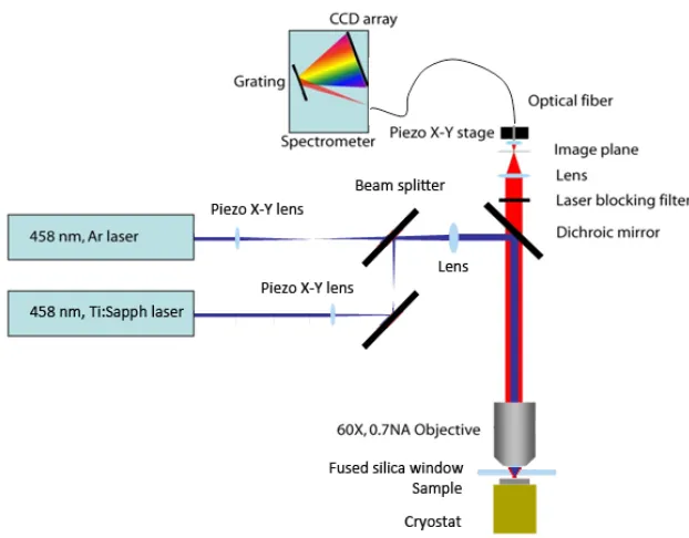
As shown in Figure 2.2, the SiO2 substrates were typically glued with silver paint
to the cold finger of a free flowing liquid nitrogen cryostat fitted with a fused silica
window (Janis), so that optical measurements in the 4.2 K-298 K temperature range could
be made. The spatially resolved photoluminescence excitation and detection setup
consisted of a homebuilt microscope using a 60X 0.7 N.A. objective (Nikon) and an f =
750 mm tube lens, giving a total optical magnification of 267X. Laser light from an
argon ion laser (Coherent MotoFred) at a wavelength of 457.9 nm was spatially filtered
and expanded to a beam of 5 mm waist and was subsequently focused on the sample by
the objective to a spot of ~800 nm waist. A frequency doubled titanium-sapphire
(Ti:Sapph) laser (Coherent Chameleon Ultra II, pulse width 140 fs, repetition rate 80
MHz) was also focused on the sample for the experiments described in Chapter 8. Using
piezoelectric translator stages (Physik Instrumente) holding the first lens in a telescope
setup, both laser spots could be moved on the sample with an accuracy of ~50 nm. The
20 off by a dichroic mirror and long wavelength pass filter combination giving a detection
wavelength range of 480-700 nm. A spatial resolution in the detection of ~500 nm could
be obtained by placing an optical fiber connected to the entrance slit of 0.3 M
spectrometer fitted with 150 and 600 g/m (Acton) gratings, at the projected sample plane
on piezoelectric translator stages. A cooled CCD camera (Pixis 2K, Princeton
Instruments) was used for detection of the dispersed light, giving a maximum wavelength
resolution of ~0.1 nm (500 µeV).
Figure 2.2: Micro-photoluminescence setup used in most optical measurements. Argon
ion and titanium:sapphire laser positions on the sample surface were computer controlled with lenses mounted on piezoelectric stages. An optical fiber mounted on a third set of piezoelectric stages in the image plane was used to send photoluminescence from specific
portions of the image output to a spectrometer. Samples were typically mounted on a cryostat and viewed under a 60X 0.7 N.A. objective.
Following optical measurements, data was converted, parsed, and analyzed using
21 programming tasks, Origin was generally used for plotting data, and COMSOL
22
References
1. Kuech, T.F. & Veuhoff, E. Mechanism of carbon incorporation in MOCVD
23
Chapter 3. Size-Dependent Waveguide Dispersion in Nanowire Optical Cavities
Reproduced in part with permission from Nano Letters, Volume 9, Issue 4, Pages 1684-1688. Copyright 2009 American Chemical Society.
Central to the appeal of utilizing semiconductor nanowires for nanophotonic
applications is their ability to confine and guide light at the nanoscale, enabling
functionalities such as optical transport,1, 2 resonators,3 lasers,4 and sensors.5 By virtue of
the high refractive index mismatch with their surroundings, semiconductor nanowires of
subwavelength width strongly confine optical waves and are ideally suited for the
development of integrated nanophotonic systems.6, 7 The various confined optical modes
propagating in dielectric nanowire waveguides are characterized by their
energy-wavevector dispersion, which theory predicts to be strongly size dependent at the
nanoscale.8 Knowledge of the size dependence of the waveguide mode dispersion is
crucial for understanding the fundamental size effects of strong optical confinement and
the optimal design of nanowire-based photonic devices where a specific dispersion and/or
group velocity dispersion may be required. For instance, in optical communication high
speed transmission with a low group velocity dispersion is desirable in order to preserve
signal pulse shapes9 whereas slowed light would, due to increased interaction times and
increased electromagnetic densities, be advantageous in optical nonlinearity based
applications10 or optical sensing.11
While the theoretical mode properties of dielectric (nano)fiber waveguides have
been elaborately treated,6, 8, 12, 13 no experimental data on the size dependence of the
waveguide dispersion of subwavelength dielectric nanowires has been reported. Direct
angle-24 resolved transmission or emission experiments14, 15 and time-resolved transmission
experiments can measure its derivative, the group velocity.16 However, for nanowires
these measurements are hindered by the scrambling effect of the subwavelength apertures
at the wire ends due to diffraction,17 the short transmission times involved10 and the
difficulty of in-coupling of the probe light with a large energy and wavevector
distribution.18
In this chapter we report on the experimentally determined strong size
dependence of optical dispersion and associated group velocities in subwavelength width
ZnSe nanowire waveguide cavities, using Fabry-Pérot resonator modes as probes over a
wide energy range. Furthermore, we observed subwavelength (λ/9) dispersionless
waveguiding and significant slowing of the propagating light by 90% (c/8). These results,
in addition to providing insights into nanoscale optical transport, will facilitate the
rational design of nanophotonic devices with dispersion and group velocity tailored
towards specific functions including optical computation,19 sensing11 and
communication.9
3.1.Experimental Procedures
ZnSe nanowires were synthesized in a quartz tube furnace using evaporation of
elemental Zn and Se powders. 4 mg of Se powder was placed in a quartz boat at 12.9 cm
upstream (referenced to the middle of the tube), 5 mg of Zn powder was placed in a
quartz boat at 9.4 cm upstream and Si substrates covered by a 5 nm thick Au/Pd layer
using plasma sputter deposition were placed 16.4 cm downstream. The tube was
25 reach a stable pressure of 50 Torr. The tube was rapidly heated to 1000 °C and kept there
for 60 minutes after which the furnace was cooled by a forced airflow. After synthesis,
the nanowires were transferred to Si substrates covered with a 300 nm thermal oxide by
dry transfer. The measurement substrates were lithographically patterned to contain
markers so that individual wires could be characterized by both electron and optical
microscopy (Figure 3.1a). Optical experiments were carried out under the
photoluminescence setup shown in Figure 2.2, using a beam expander/spatial filter to
enlarge the Ar+ laser excitation spot to around 1 mm, giving an average excitation power
density of 4 W/cm2. Detail of the experimental geometry is shown in Figure 3.1b.
Photoluminescence from the individual wires was spatially and spectrally resolved using
the methods discussed in Chapter 2. After optical measurements, the lengths (+/-20 nm)
and widths (+/-4 nm) of the nanowires were determined by Scanning Electron
Microscopy (FEI Strata DB235 FIB) with the widest part of the wire taken as the width
(diameter) i.e. ignoring any faceting.
A photoluminescence image of a nanowire (Figure 3.1c) shows, in addition to
emission from the nanowire body, pronounced emission from the end facets. Further
investigation of the nature of the body and end emission by spatially resolving the spectra
shows that the emission from the nanowire body (Figure 3.1d, black trace) consists of a
broad peak centered at 2.15 eV in addition to minor band-edge emission centered at 2.65
eV, characteristic of ZnSe defect emission caused by interstitial Zn ions and exciton
recombination respectively.20 The emission spectra obtained from the nanowire ends
however show a pronounced modulation over a wide spectral range (Figure 3.1d, red and
26 (Figure 3.1d, right inset) demonstrating that the nanowire functions as an optical
Fabry-Pérot resonator along its length.
Figure 3.1: a) Scanning electron microscopy image of a ZnSe nanowire dispersed onto a
300 nm thick SiO2 covered Si wafer. Scale bar, 2 µm. b) experimental geometry
whereby the nanowire is uniformly excited perpendicular to its long axis. c) real color optical image of the emission of a ZnSe nanowire under uniform laser illumination. Scale
bar, 2 µm. d) Typical emission spectra collected at the middle part of the nanowire (lower trace, black) and from the end of a 7.77 µm short nanowire (middle trace, red) and
at the end of a 44.82 µm long wire (upper trace, blue) shows Fabry-Pérot modes of the nanowire resonator. A magnification of the upper trace is shown in the left inset. (Right
inset) mode spacing at 2.1 eV for nanowires of comparable widths as a function of their reciprocal length, fitted by a least squares linear fit.
As introduced in Section 1.3, the internally generated light is confined due to the
large refractive index mismatch between the nanowire and its surroundings and is
27 nanowire is sufficiently high and the losses along the length of the wire are sufficiently
low, standing optical waves can develop, giving rise to interference peaks in the spectrum
of the leaked light at the nanowire ends. In wavevector space these interference peaks are
equally spaced at integral multiples of π/Lz (Lz, wire length).21 Thus, by plotting the peak
positions in the energy space versus incremental wavevector multiples of π/Lz, the shape
of the energy-wavevector dispersion can be determined. Since our measurements are
obtained in the far-field, the absolute values of the parallel wavevectors cannot be
determined. However, by comparison with theoretical calculations based on the
numerical solutions of the Maxwell’s equations for the measured nanowire, precise
assignment of the absolute parallel wavevectors and the waveguided mode-type (e.g.,
hybrid-electric, transverse-electric) can be made, which also helps to identify novel
nanowire dispersion features owing to their small diameters.
3.2.Numerical calculations
In order to calculate the allowed photonic modes in our nanowires, we simplified
the wire geometry to a cylindrical one with a homogeneous refractive index profile inside
the ZnSe core and an air cladding so that analytical expressions can be used. Since the
observed interference phenomena are due to light propagating along the length of the
wires, in the z-direction (confined by the surface in x and y) we calculated the mode
dispersion in this direction. The propagation constant β of confined waveguide modes of
a step index profile dielectric cylinder waveguide can be calculated using the following
28 magnetic TMνm and hybrid EHνm HEνm modes, where the subscript ν denotes the order
and the subscript m denotes the mth root:
HEνm EHνm:
0 ) ( ) ( ) ( ) ( 0 1 0
1 + =
W UK W K U UJ U
J Eq. 3.1
TE0m: ' 2 4
2 2 ' ' ' ) ( ) ( ) ( ) ( ) ( ) ( ) ( ) ( = + + UW V kn W UK W K n n U UJ U J W UK W K U UJ U J co co
cl νβ
ν ν ν ν ν ν ν
ν Eq. 3.2
TM0m :
0 ) ( ) ( ) ( ) ( 0 1 2 0 1 2 = + W UK W K n U UJ U J
nco cl Eq. 3.3
With: = 2 2 −β2
co n k r
U Eq. 3.4
2 2 cl co n n rk
V = − Eq. 3.5
2 2 2 cl n k r
W = β - Eq. 3.6
and J the Bessel function of the first kind, K the modified Bessel function of the second
kind, r the cylinder radius, k the free space wavevector, λ the free space wavelength nco
the core refractive index and ncl the cladding refractive index. These equations were
made specific for the ZnSe material by the inclusion of the known dispersion of the
refractive index of ZnSe. The calculated propagation constant β can in general be
complex; therefore in this chapter kz was used to denote the real solutions of the
29 obtained by setting the waveguide parameter V (optical frequency normalized to the
waveguide radius) equal to 2.40512. The group velocity (∂ω/∂kz) was obtained by
numerically differentiating the obtained mode dispersions. Since the obtained
experimental data points consist of relative kz values, typically an offset amount
consisting of an integer number of (π/Lz) was added to the relative kz values in order to
obtain the absolute mode wavevectors.
3.3.Discussion
In order to examine the influence of the nanowire width on the mode dispersion,
emission spectra were taken from the ends of nanowires with varying width as
determined by SEM (Figure 3.2a). Figure 3.2b shows the spectra of these wires with
radii of 110 nm, 100 nm, 90 and 80 nm. Aside from the different interference peak
spacings caused by the different wire lengths, the spectra show a decrease in the
modulation intensity towards lower energy, eventually leading to smooth and
unmodulated spectra. This low energy cutoff, as is indicated by arrows, shifts to higher
energy with a decrease of the nanowire width. A plot of the measured interference peaks
as a function of incremental wavevector steps for the four different nanowires of different
diameters is shown in Figure 3.2c. The solid lines represent the solutions of the
numerically solved eigenvalue equation of an air-clad dielectric cylinder waveguide8 with
the measured nanowire radius and the energy-dependent refractive index as determined
from a bulk ZnSe crystal,22 as input parameters. The nanowire width dependence of the
measured mode dispersion and their cutoffs corresponds well with the lowest order mode