http://www.sciencepublishinggroup.com/j/ajece doi: 10.11648/j.ajece.20190301.15
ISSN: 2640-0480 (Print); ISSN: 2640-0502 (Online)
An Efficient Fault Detection of FPGA and Memory Using
Built-in Self Test [BIST]
Mahesh Kumar
Department of Electronics, PSG College of Arts & Science, Coimbatore, India
Email address:
To cite this article:
Mahesh Kumar. An Efficient Fault Detection of FPGA and Memory Using Built-in Self Test [BIST]. American Journal of Electrical and Computer Engineering. Vol. 3, No. 1, 2019, pp. 38-45. doi: 10.11648/j.ajece.20190301.15
Received: November 29, 2018; Accepted: January 5, 2019; Published: July 2, 2019
Abstract:
In this paper, a new technique for localization of fault detection and diagnosis in the interconnects and logic blocks of an arbitrary design implemented on a Field-Programmable Gate Array (FPGA) using BIST is presented. This technique can uniquely identify any single bridging, open or stuck-at fault in the interconnect as well as any single functional fault, a fault resulting a change in the truth table of a function, in the logic blocks. The test pattern generator and output response analyzer are configured by existing CLBs in FPGAs; thus, no extra area overhead is needed for the proposed BIST structure. The scheme also rests on partitioning of rows and columns of the memory array by employing low cost test logic. It is designed to meet requirements of at-speed test thus enabling detection of timing defects. Experimental results confirm high diagnostic accuracy of the proposed scheme and its time efficiency.Keywords:
Fault Diagnosis, Built-in Self-Test (BIST), Configurable Logic Block (CLB), Field-Programmable Gate Array (FPGA), Testing1. Introduction
Field-Programmable Gate Arrays (FPGAs) are 2-D arrays of Configurable Logic Blocks (CLBs) and programmable switch matrices, surrounded by programmable input/output blocks on the periphery. FPGAs are widely used in many
applications such as networking, storage systems,
communication, and adaptive computing, due to their reprogrammability, flexibility, and reduced time-to-market. The reprogrammability of FPGAs results in faster design and debug cycle compared to Application-Specific Integrated Circuits (ASICs). However, once the design is finalized and fixed, the programmability becomes useless and costly, if infield further customization and reprogrammability are not required. In order to reduce the manufacturing costs associated with FPGAs, application-specific FPGAs have been introduced in the FPGA industry which restricts the use of the FPGA device for only one application (design). Xilinx’s Easy path solution is an example [1]. The cost reduction is mainly due to using devices that may contain defects in the areas not used by the particular application. This, in turns, increases the manufacturing yield compared to the traditional scenario in which any defective device is
thrown away.
During the system operation, application-dependent test and diagnosis are very crucial in online self-repair schemes for fault tolerant applications [2]. In these applications, the existence of faults in the system is first identified and then the faulty resources are precisely diagnosed. After that, the design is remapped to avoid the faulty resources occurring in it. Because of that the test and diagnosis procedures are performed during the system operation (online), the number of test vectors and configurations must be minimized. Note that the test time is dominated by loading the exact test configurations rather than applying test vectors. Compared to independent test and diagnosis, application-dependent test and diagnosis provides faster test and diagnosis time while achieving a higher diagnosis resolution over a more comprehensive fault list. This is because application-dependent test and diagnosis focus only on the FPGA resources used for that particular design, rather than all FPGA resources.
in a small number of test configurations. For logic diagnosis, a Built-in Self Diagnosis (BISD) method is presented in which the configuration of used logic blocks remains unchanged while the configurations of the interconnect resources and unused logic blocks are modified. Any single functional fault, inclusive of all stuck-at faults, in logic blocks is precisely diagnosed in only one test configuration.
The use of memory cores in SOC designs is rising quickly. As memory cores are dominating the silicon area of typical SOC designs, and the density of memory circuits is normally higher than logic circuits, the chip yield is mainly determined by the memory yield. To improve the chip yield, whether by process enhancement or design improvement, diagnosis of the memory cores after testing is necessary. Embedded memory testing is normally done by Built-in Self-Test (BIST) [3, 4]. A BIST scheme that also collects and exports the diagnostic data for subsequent online or offline analysis has been called a Built-in Self-Diagnosis (BISD) scheme [5, 6].
Just as test data compression for logic circuits, memory test data compression has also received attention recently. In [7], the bit-maps for large memories are compressed by using fail patterns. Another work considers the compression of the output response of the BIST circuit [8]–[10]. The method is similar to signature analysis in logic BIST. The BIST circuit may export the test information, called fault-syndrome, to test for failure analysis. The size of fault-syndrome affects total test cost directly.
However, except diagnosis data compression, using a redundancy repair approach to enhance memory yield is the other important issue in recent years. It has become imperative to deploy effective means for testing and diagnosing non-volatile memory failures. A functional model employed for these memories remains similar to that of RAMs with relevant fault types such as stuck-ats and bridges being tackled through functional test algorithms [11]. Also, all addressing malfunctions are covered by memory cell stuck-at fault tests as there are no overwrites in the mission mode. Typically, the basic test reads successive memory cells, and processes output responses by performing a polynomial division to compute a cyclic redundancy code (signature). The same procedure can be used to detect certain classes of dynamic faults provided memory cells are designed with additional DFT features [12].
A novel BIST design with comprehensive on-the-fly exhaustive redundancy search and analysis method is presented in [13], which allows on-chip optimal redundancy allocation without having to construct the complete failed bitmap. It however has high hardware overhead for a reasonably big number of spare (redundant) elements. We find the failure patterns into three types: faulty words, faulty rows, and faulty columns. The faulty row/column is the continuous faults on the same row/column. Different fail patterns exhibit different syndrome characteristics. The built-in syndrome compressor is designed to efficiently compress the fault syndromes. Our approach reduces the amount of data that needs to be transmitted from the chip under test.
Moreover, the proposed method does not increase the test time for the fault-free memories. It results in a much shorter diagnosis time than the conventional BISD schemes. Simulation results for memories under various fault pattern distributions show that in most cases the data can be compressed to less than that of its original size. Furthermore, based on fail pattern identification technique, the faulty row/column can be replaced by redundancy row/column. Therefore, the complexity of RA algorithms can be reduced. An acceptable RA algorithm for BIST implementation should be considered not only for the repair efficiency but also the hardware overhead of the BISR circuit.
2. Basic BIST Architecture
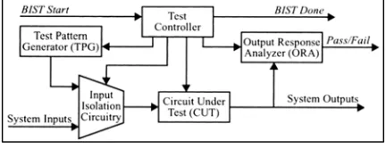
A representative architecture of the BIST circuitry as it might be incorporated into the CUT is illustrated in the Figure 1. This BIST architecture also includes two essential functions as well as two additional functions that are necessary to facilitate execution of the self-testing feature within the system.
Figure 1. Basic BIST Architecture.
The two essential functions include the Test Pattern Generator (TPG) and Output Response Analyzer (ORA). While the TPG produces a sequence of patterns for testing the CUT, the ORA compacts the output responses of the CUT into some type of Pass/Fail indication. The other two functions needed for system-level use of the BIST include the test controller (or BIST controller) and the input isolation circuitry. Aside from the normal system I/O pins, the incorporation of BIST may also require additional I/O pins for activating the BIST sequence (the BIST Start control signal), reporting the results of the BIST (the Pass/Fail indication), and an optional indication (BIST Done) that the BIST sequence is completed and that the BIST results are valid and can be read to determine the fault-free/faulty status of the CUT.
3. FPGA Fault Detection
resources are addressed in this section. For inter-CLB interconnect test and diagnosis, the configuration of routing resources remains unchanged while the configuration of logic resources are modified.
Figure 2. FPGA Architecture.
Test and diagnosis of intra-CLB interconnects along with logic resources are also discussed. For this purpose, the configuration of used logic resources (inclusive of intra-CLB interconnects) is kept unchanged whereas the configuration of inter-CLB interconnects as well as unused logic resources are changed. The separation between inter-CLB and intra-CLB is made because in contemporary FPGAs the programmable logic resources are not limited to lookup tables (LUTs); other logic resources such as carry generation/propagation logic and cascade chains are included in CLBs. For inter-CLB interconnect test and diagnosis, these logic elements, if used in the original configuration, will be bypassed.
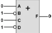
A single-term function F is a logic function which has only one minterm or only one maxterm. In other words, the truth table of a single-term function consists of only one minterm or one maxterm. The input pattern corresponding to that minterm (or maxterm) of function F is called Activating Input (AIF).
Figure 3. Single-term Function with Activating Input Pattern.
A single-term function can be viewed as an AND (OR) function with possible inversions at the inputs and/or output. For a single-term function, if the applied input vector is the activating input, all sensitized faults are detected. An example is shown in Figure 3, which has only one maxterm.
Since the activating input (0101) is applied, A/1 (A stuck-at 1 fault), B/0, C/1 and D/0 are detected. Moreover the bridging faults between A and B are also detected. It should be noted that if a bridging fault is sensitized, i.e., two nets
have opposite values, detection under various bridging fault models, namely wired-OR, wired-AND, and dominant, is guaranteed. This is because the value of at least one of the signals is modified and the condition of single-term function and activating inputs guarantee the propagation of faulty value(s) to the reachable primary output(s).
Detection of feedback bridging faults requires logic-level sensitization and propagation of the fault. In addition to that, depending on the polarity of feedback path, which may result in oscillation, some extra timing conditions must be satisfied. The use of single term functions guarantees the logic-level requirements of such detection.
Single-term functions guarantee the detection of all sensitized faults. However, some mechanism is required to sensitize all faults in the fault list. We implement single-term functions in all used LUTs in the design. By implementing different single-term functions in used logic blocks such that each fault in the fault list is sensitized in at least one test configuration, all faults can be detected. Since these test configurations target faults in inter-CLB interconnect, all additional logic resources in CLBs, if used, will be bypassed. Hence, CLBs are configured as LUTs followed by flip-flops. The following subsections describe the proposed diagnosis procedures based on various fault models.
(1) Diagnosis of Stuck-At Faults: A circuit with ‘n’ nets has 2n stuck-at faults. Based on the above assumption, in order to uniquely identify any single stuck-at fault at least log22n = 1 + log2n test configurations are required.
(2) Diagnosis of Open Faults: An open fault on a net can be detected by applying a sequence of stuck-at fault tests for that net. Since an open fault can behave either as stuck-at-1 or stuck-at-0 faults, it is required to test for both stuck-at faults to guarantee the detection of open faults. If the logic behavior of an open is equivalent to a 1 (or stuck-at-0) fault, then the diagnosis procedure identifies the open as a stuck-at-1 (or stuck-at-0) fault due to fault equivalency.
(3) Diagnosis of Bridging Faults: The bridging fault list for ‘n’ a circuit with net contains n(n-1)/2 distinct pair-wise bridging faults. Hence, at least log2 [n(n-1)]/2 = 2log2 n-1 test configurations are required for single bridging fault diagnosis.
each LUT in the FPGA.
4. Configuration Logic Block Detection
For logic block (including intra-CLB interconnects) testing and diagnosis, the configuration of the original used logic blocks is preserved while the configuration of interconnects and unused logic blocks are changed to exhaustively test and diagnose all used logic blocks. This is in contrast to the method presented in the previous section for interconnects in which the configurations of used CLBs are replaced by appropriate single-term functions.
Figure 4. Application-dependent Self-test Architecture for Logic Blocks (a) Original Configuration (b) BIST Configuration.
The idea of application-dependent logic block testing is presented in [16]. In this BIST scheme, each used logic block is exhaustively (or super-exhaustively, i.e., all possible transitions) tested while all these logic blocks are tested concurrently. The global interconnect is reprogrammed in such a way that the test signals are routed to each logic block. A Linear Feedback Shift Register (LFSR) or a binary counter for generating test vectors is connected to the inputs of all used logic blocks. The logic block outputs are observed through an internal response compactor (e.g., an XOR tree). The response compactor can be combined with a response (parity) predictor, as will be explained shortly, such that a unique pass/fail signal can be generated. The LFSR and the XOR tree are implemented in the available unused logic blocks. Since the LFSR or binary counter generates all possible patterns (2n patterns for an-input logic block) and the XOR tree propagates any single fault to its output, any single functional fault in the used logic blocks are propagated to the output of the XOR tree and is detected. Functional faults is any fault that changes the truth-table of an LUT, including stuck-at faults.
Figure 4 shows an example of this scheme. In Figure 4(a) the original design, with used logic blocks F1 to F9 with
original interconnections, is shown. In the BIST
configuration, the original interconnections are modifies such that LFSR outputs, implemented in unused blocks, are connected to the inputs of all used blocks F1-F9 in parallel. The outputs of used blocks along with the parity predictor block are connected to the response compactor, which is also implemented in the available unused resources. The classical XOR tree does not provide any diagnosis capability. In order to improve the diagnostic resolution of this scheme, a
combinational compactor based on error correcting schemes can be exploited instead of the XOR tree. If a compactor with more than one output is used and logic block outputs are selectively connected to the compactor outputs (through the network of XOR gates), the failing pattern at the outputs of the compactor can identify failing logic block(s). Test patterns generators (TPGs), such as LFSR, and Output Response Analyzers (ORAs) have been used in the context of FPGA BIST [17, 18, 19, 20, 21]. However, the use of parity/checksum precomputation (which requires only one LUT/block rather than a full XOR-tree) and response comparator which uniquely codes the failing block(s), particularly in the context of application-dependent diagnosis, is novel.
5. Fail Pattern Identification in Memory
In this work, the BIST and BISR design are based on fail pattern identification, and this section describes the fail-pattern identification scheme in detail. A defect in different parts of the memory may lead to different faults and/or fail patterns [22, 23, 24]. Fault identification is not trivial, and can be aided by using the fail pattern information. We will describe the approach to distinguish the fail patterns during the test process.
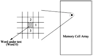
Figure 5. Memory Cell Array Being Tested.
Figure 5 shows the memory cell array being tested. The shaded region represents the Word Under Test (WUT). If the WUT has a different output than the expected value when we read it, then the word fails and a fault is detected. In a typical BISD design, when a fault is detected the test process pauses, and the fault data is either registered or shifted out before the test process resumes. However, whether it is shifted out immediately or registered and then shifted out later, the cost (time complexity and ATE capture memory size) can be high if there are many faults. We use a more advanced approach, i.e., identify the faulty rows, faulty columns, and faulty words simultaneously during the test process.
1. Faulty Row: When the WUT is faulty, we test the next
word in the same row, i.e., Word 1 as shown in Figure 1. If Word 1 is also faulty, we continue to test the next word in the same row until we reach a fault-free word or the end of the row.
several condition-checking steps.
a. Word 1 is tested fault free, so a faulty row can be excluded.
b.The word above the WUT in the same column (i.e., Word 2 as shown in Figure 1) is tested fault free; otherwise the WUT has been covered by the previous faulty column test.
c. The word under the WUT in the same column (i.e., Word 3 as shown in Figure 1) is tested faulty. We continue to test the subsequent words in the same column until we reach a fault-free word or the end of the column.
3.Single Faulty Word: When the WUT is faulty but not in
a faulty row or column, i.e., Word 1, Word 2, and Word 3 are all tested fault-free, we consider the WUT as a single faulty word.
This process does not increase the test time for a fault-free memory, because the test algorithm is the same as in the original BIST design. If the memory is faulty, then there will be a slight time penalty for fail pattern identification. However, compared with original BISD scheme, the size of
memory diagnosis data to be exported and the total test data diagnosis time can be reduced greatly. Considering BISR applications, the fail pattern identification approach can replace the must-repair phase and the time penalty can be compensated by RA time reduction.
Diagnosis Syndrome Format
The proposed fault syndromes for the three fail patterns, as well as the original syndrome, are shown in Figure 5. The original syndrome is composed of three fields-sessions, address, and word syndrome. The Session field records the Read operation that detects the fault. The Address field stores the address of the faulty word, so its length is equal to the length of a normal word address. The Word Syndrome field stores the compressing word syndrome of the faulty word at the current state, which represent the faulty cells in this word. The proposed syndrome for single faulty word has four fields-Syndrome ID, Session, Address, and Compressed Word Syndrome. The Syndrome IDs are used to distinguish the fail patterns: 00, 11, and 01 represent the single faulty word, row fault, and column fault, respectively.
Figure 6. Simulation for Single-term Function.
The Faulty-Row syndrome is composed of four fields. It does not include the Word Syndrome, but it needs to record the addresses of the first and last faulty words. Since the last faulty word has the same row address with the first faulty word, we only need to store the column address of the last faulty word (the End Column field). The Faulty-Column syndrome is similar to the Faulty-Row syndrome, except that it has the Compressed Word Syndrome field. Since all words are in the same column, only the address of the last faulty word in the column is recorded in the End Row field. Because the memory is
increase to identify different fault types. In this manuscript, we target on three typical fault types: row, faulty-column, and faulty word.
If the memory is fault-free, the Sequencer will only run in the Test Execution states, i.e., BIST Idle, BIST Apply, and BIST Done. It will then look like a typical BIST design, and in this case the testing time does not increase.
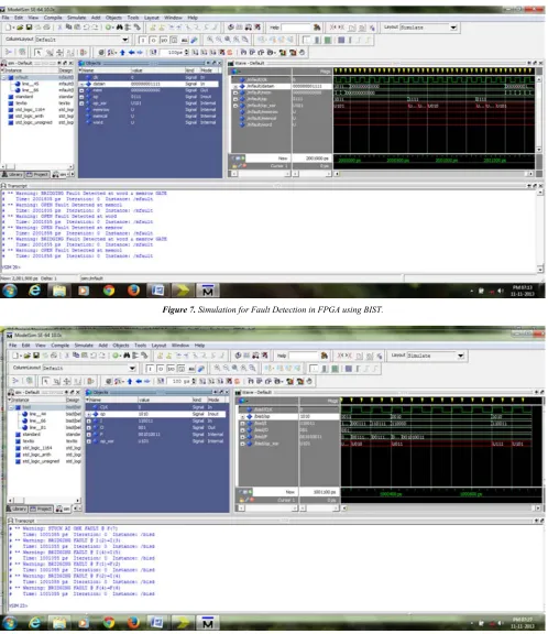
6. Simulation Result
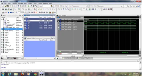
Simulation result for the Figure 3 single term function without applying the BIST is shown in the Figure 6 same thing for the fault detection in the CLBs and also in the memory using BIST as shown in the Figure 7 and 8.
Figure 7. Simulation for Fault Detection in FPGA using BIST.
7. Conclusion
A new BIST approach for fault detection and diagnosis of FPGAs and memory has been proposed in this paper. The proposed FPGA BIST structure has high fault coverage on the modelled interconnect and CLB faults, including short/open and delay faults in wire channels, stuck on/off faults in PSs, and stuck-at-0/1 faults in LUTs. The test results for various FPGAs have shown that adequate performance in fault coverage, test time, and area overhead can be achieved by using the proposed BIST structure. The proposed FPGA BIST structure possesses the ability to simultaneously detect and diagnose faults on both interconnect resources and CLBs. For interconnect diagnosis, multiple faults (open, stuck-at, or bridging fault) can be uniquely identified.
References
[1] Xilinx Inc., San Jose, CA, “Xilinx EasyPath Solutions,” 2006. [Online]. Available: www.xilinx.com.
[2] W. -J. Huang and E. J. McCluskey, “Column-based precompiled configuration techniques for FPGA fault tolerance,” in Proc. IEEE Symp. Field-Program. Custom Comput. Mach., 2001, pp. 137–146.
[3] C. T. Huang, J. -R. Huang, C. -F. Wu, C. -W. Wu, and T. -Y. Chang, “A programmable BIST core for embedded DRAM,” IEEE Des. Test Comput., vol. 16, no. 1, pp. 59–70, Jan.–Mar. 1999.
[4] L. -T. Wang, C. -W. Wu, and X. Wen, Design for Testability: VLSI Test Principles and Architectures. San Francisco, CA: Elsevier (Morgan Kaufmann), 2006.
[5] R. P. Treuer and V. K. Agarwal, “Built-in self-diagnosis for repairable embedded RAMs,” IEEE Des. Test Comput., vol. 10, no. 2, pp. 24–33, Jun. 1993.
[6] C. -W. Wang, C. -F. Wu, J. -F. Li, C. -W. Wu, T. Teng, K. Chiu, and H. -P. Lin, “A built-in self-test and self-diagnosis scheme for embedded SRAM,” J. Electron. Test.: Theory Appl., vol. 18, no. 6, pp. 637–647, Dec. 2002.
[7] J. Vollrath, U. Lederer, and T. Hladschik, “Compressed bit fail maps for memory fail pattern classification,” in Proc. IEEE Euro. TestWorkshop (ETW), 2000, pp. 125–130.
[8] V. N. Yarmolik, S. Hellebrand, and H. Wunderlich, “Self-adjusting output data compression: An efficient BIST technique for RAMs,” in Proc. Conf. Des., Autom., Test Euro. (DATE), 1998, pp. 173–179.
[9] S. Hellebrand, H. Wunderlich, A. Ivaniuk, Y. Klimets, and V. N.Yarmolik, “Error detecting refreshment for embedded DRAMs,” in Proc. IEEE VLSI Test Symp. (VTS), 1999, pp. 384–390.
[10] S. Hellebrand, H. Wunderlich, A. Ivaniuk, Y. Klimets, and V. N.Yarmolik, “Efficient online and offline testing of embedded DRAMs,” IEEE Trans. Comput., vol. 51, no. 7, pp. 801–809, Jul. 2002.
[11] A. K. Sharma, Semiconductor Memories: Technology, Testing and Reliability. New York: Wiley, 2002.
[12] Y. -H. Lee, Y. -G. Jan, J. -J. Shen, S. -W. Tzeng, M. -H. Chuang, and J. -Y. Lin, “A DFT architecture for a dynamic fault model of the embedded mask ROM of SoC,” in Proc. Int. Workshop Memory Technol. Design Testing, 2005, pp. 78–82.
[13] T. Kawagoe, J. Ohtani, M. Niiro, T. Ooishi, M. Hamada, and H. Hidaka, “A built-in self-repair analyzer (CRESTA) for embedded DRAMs,” in Proc. Int. Test Conf. (ITC), 2000, pp. 567–574.
[14] S. R. Patil, D. B. Musle, “Implementation of BIST technology for fault detection and repair of the multiported memory using FPGA”, International conference of Electronics, Communication and Aerospace Technology (ICECA), December 2017.
[15] M. B. Tahoori, “Diagnosis of open defects in FPGA interconnects,” in Proc. IEEE Int. Conf. Field-Program. Technol., 2002, pp. 328–331.
[16] M. B. Tahoori, “Application dependent testing of FPGAs,” IEEE Trans. Very Large Scale Integr. (VLSI) Circuits, vol. 14, no. 9, pp. 1024–1033, Sep. 2006.
[17] M. Abramovici and C. Stroud, “BIST-based detection and diagnosis of multiple faults in FPGAs,” in Proc. Int. Test Conf., 2000, pp. 785–794.
[18] A. Doumar and H. Ito, “Detecting, diagnosing, and tolerating faults in SRAM-Based field programmable gate arrays, a survey,” IEEE Trans. Very Large Scale Integr. (VLSI) Syst., vol. 11, no. 3, pp. 386–405, Mar. 2003.
[19] W. Quddus, A. Jas, and N. A. Touba, “Configuration self-test in FPGA based reconfigurable systems,” in Proc. ISCAS, 1999, pp. 97–100.
[20] C. Stroud, E. Lee, and M. Abramovici, “BIST based diagnostics of FPGA logic blocks,” in Proc. Int. Test Conf, 1997, pp. 539–547.
[21] C. Stroud, S. Konala, C. Ping, and M. Abramovici, “Built-in self-test of logic blocks in FPGAs (Finally, a free lunch: Bist without overhead!),” in Proc. VLSI Test Symp., 1996, pp. 387–392.
[22] J. T. Chen, J. Khare, K. Walker, S. Shaikh, J. Rajski, and W. Maly, “Test response compression and bitmap encoding for embedded memories in manufacturing process monitoring,” in Proc. Int. Test Conf. (ITC), 2001, pp. 258–267.
[23] Anita Aghaie, Mehran Mozaffari Kermani, Reza Azarderakhsh, “Reliable and Fault Diagnosis Architectures for Hardware and Software-Efficient Block Cipher KLEIN Benchmarked on FPGA”, IEEE Transactions on Computer-Aided Design of Integrated Circuits and Systems, Volume 37, Issue 4, April 2018, pp 901 – 905.