Process Variation Aware FINFET based Digital Circuits Design
Shikha Rai1, Umesh Dutta21[email protected] Electronic & communication engineering
Manav Rachna International University, Faridabad, India
Abstract:- Finfet is a major device which is used for constructing an electronic circuit. It reduces the short channel effect and increases the chip area and density of transistor. In this paper, the objective is to increase the drive current by varying all the parameters of the device like the height of the fin, oxide thickness, doping concentration, and finding the better result by parameter variation. SRAM has become a major component in many VLSI chips due to its high storage density and small access time. SRAM can be used in many electronic gazets because of its low power and low voltage memory design. In recent years due to increased demand for notebooks, laptops, IC memory cards SRAMs are extensively used as both on chip and off-chip memories, because of their ease of use and low standby leakage current. The main objective of this paper is to evaluate the performance in terms of Power consumption, delay and SNM of existing 6T CMOS SRAM cell in 32nm and 22nm technology.
KEYWORDS:- Finfet device, SRAM , PVT, Variability, Transistor sizing.
I. INTRODUCTION
Tri- gate FinFET is one of the most desirable alternative structures to be used on the industry scaling for future technology generations of 32 nm and beyond [1].The tri-gate FinFET provides a symmetric device structure where the channel is linked by gate from three sides of the Si film. Since the gate control is increased, the need on the Si film thickness is used as compared to single gate or double gate FinFET. Compared to double gate FinFET, the Tri-gate FinFETs are better due to the increased gate control over the channel. So we can efficiently reduce the short channel effects and also further scaling is possible to meet the requirements. Several FinFET devices have been launched which can be used as replacement for CMOS transistors. In a FinFET transistor, the channel electrical potential is controlled by the voltage at the gate. Effectively, this reduces the SCE compared to CMOS transistors [5]. Another advantage of the FinFET is that the traditional MOSFET fabrication processes can be used. Fig. 1 shows the structure of a traditional tri-gate FinFET as developed by Intel. Here, the fin acts as a channel and terminates on both sides of the source and drain. A metal gate is formed over the Si
substrate, which controls the channel. Straddling of a metal gate over a Si-fin gives efficient gate-controlled characteristics compared to MOSFET. Since the gate straddles the fin, the length of the channel is the same as the width of the fin. As there are effectively two gates around the fin, the width of the channel is twice the height of the fin. The height of the FinFET is equivalent to the width of the MOSFET. In order to attain the same area efficiency, the height of the fins should be half the fin pitch width.
Fig 1 structure of Intel’s tri-gate FinFET [6]
II. LITERATURE REVIEW
efficient SRAM cells (6T and 5T) based on adiabatic principles and design modifications. Bulk of the energy in SRAMs is wasted during charging of the bit lines and discharging it to the ground during read and writes operations. It is proposed to use adiabatic approach to collect this energy and recycle it. Based on this thought process a separate and simple adiabatic driver circuit has been designed and used for bit line charging. It is shown that in 6T SRAM, a total energy of the order of 50% over a given period and around 80% during write cycle can be saved by the help of this driver.
III. DEVICE DESIGN AND SIMULATION
This work calculates the impact on ION and IOFF currents of variations in process parameters for a set of predictive FinFET technologies from 32 nm to 22 nm. The main contribution of the present study is to identify relevant behavioral standards with respect to the use of FinFET technology in digital designs. In 22nm FinFET technology, the different parameter of the device has been varied to make the device much more efficient in terms of derive current. It is no longer enough to focus only on the threshold voltage fluctuations in the development of projects and TCAD tools considering the FinFET technology. It is necessary that TCAD tools and designers evaluate all electrical characteristics/ Parameters variation of the device:
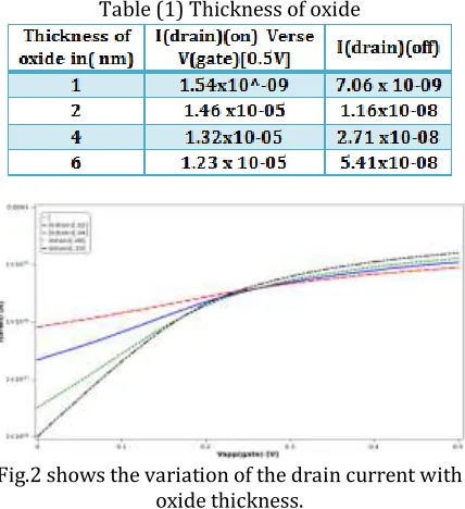
Table (1) Thickness of oxide
Fig.2 shows the variation of the drain current with oxide thickness.
The simulation carried out at different values of oxide thickness: 1nm, 2nm, 4nm, 6nm. It is seen that the ON current magnitude decreases with increase in the oxide thickness. The primary reason for this
effect is the reduction in the value of effective electric field across the oxide.
ℇox=1/ (tox)
If oxide thickness (tox) increases, ON current decreases, off current is also increased because of reduction in effectiveness of the gate to channel coupling. Because of increase in the oxide thickness the gate terminal has less effective control on the channel due to increased oxide thickness & this is a primary cause for increase in the OFF current.
Table (2) Height of fins
Fig.3 shows the variation of the drain current with height of fins.
The simulation is carried out at different values of fin height: .02um, .04um, .06um, .10um. It is seen that if the fins height is increased, drain current also increases. OFF current is reduced and device becomes more efficient and gain is improved.
Table (2) Doping concentration
value, of oxide thickness, fins height, and doping concentration. And the objective is to increase the derive current and reduce the OFF current by varying the above parameters. The table below is the optimized result.
Fig. 4 shows the variation of drain current with doping concentration of finfet device.
Table.4 Final optimized result of Finfet (22nm)
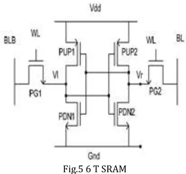
IV. 6T SRAM CIRCUIT DESIGN AND OPERATION
SRAM is a volatile memory it can retain data value as long as power supply has been ON. It is very reliable, and can easily access the data. In SRAM, Bit 0 or 1 is stored using two cross coupled inverters.
Fig.5 6 T SRAM
The cell has two stable states either 0 or 1 which is stored due to cross-coupling. There are two access transistors which are used to access the control during Read and Write operation. A 6T SRAM cell is required to optimize the device parameter to make the efficient SRAM using Read Delay, Write Delay, Leakage Power or SNM. Bit line is used for both read operation and write operation. The bit line is used to improve the noise margins. During Read cycle the bit lines become high and low by the inverter in the SRAM. Proper optimization of the Finfet parameter is needed to reduce the power dissipation, leakage power and this improves the stability. By increasing thickness of fins leads to reduction in Vd.
4.1. Standby mode (ckt in idle condition)
In standby mode word line is not active (word line=0), pass transistors PG1 and PG2 which connect 6T cell from bit lines are turned off. It means that cell cannot be processed. The two cross coupled inverters formed by PDN1- PDN2 will continue to feedback each other, till they are connected to the supply, and data will hold in the latch.
4.2. Read Mode (the data has been requested)
In read mode word line is active (word line=1). Word line enables both the pass transistor which will connect cell from the bit lines. Now values stored in nodes (node vla and vr) are transferred to the bit lines. Assume that 1 is stored at node vl so bit line will discharge through the driver transistor (PDN1) and the bit line will be pulled up through the Load transistors (PUP1) toward VDD, a logical 1. Design of SRAM cell requires read stability (do not disturb data when reading).
4.3. Write Mode (updating the content)
FINFET BASED SRAM PERFORMANCE MATRICS:- SNM: The immunity of the cell to tolerate the switching into read operation is characterized by static noise margin (SNM).It is calculated through largest side of the square which is drawn inside the butterfly characteristic of the cross coupled inverter of SRAM. During the read operation(BL = BLB =Vdd) and WL =Vdd) SNM is the parameter to measure the stability of SRAM Bit cells. The SNM depends on the variation of Vth of transistor. If the value of Vth is high, the drive current is low making the write operation more difficult and it will increase the SNM. This problem is resolved by using high Vth device which can provide with a high derive current, higher SNM along with good writing stability. The SNM is most sensitive to threshold voltage fluctuation in the access & pull-down NMOSs and less sensitive to pull-up P-Finfet device. Read Delay: Read Delay occurs in allowing the bit line to discharge upto 10% of the peak value or the delay between the application of the WL signal and the response time of the sense amplifier.
Write Delay : Write Delay is a delay time between the activation of 50% of WL to when Qbar is 90% of its full swing. Propagation delay of INV1 and INV2 can find the write delay of SRAM. Data is applied to the bit line (BL and BLB) which is written into the cell. If desired voltage is applied into a bit line and word line is activated the node will get the value from the bit line. The access transistor is activated by applying the signal to the gate or applying logic ‘1’ to word line WL. When sufficient voltage is applied at bit lines the word line is enabled and the node will get the value from the bit line.
Table (4)Parameter of 6T SRAM Circuit
Leakage Current: Leakage current flows due to minority carriers. If the gate to source voltage Vgs is less than the threshold voltage Vt (Vgs < Vt ) then the current flow from drain to source constitutes sub- threshold leakage. The drain current depends exponentially on the gate to source voltage in sub – threshold region and is given by eq (1)Id=
exp(Vgs/Vt) where Vt =KT/Q………(1) Leakage current flows when transistor is in OFF state.
V. RESULT AND DISCUSSION
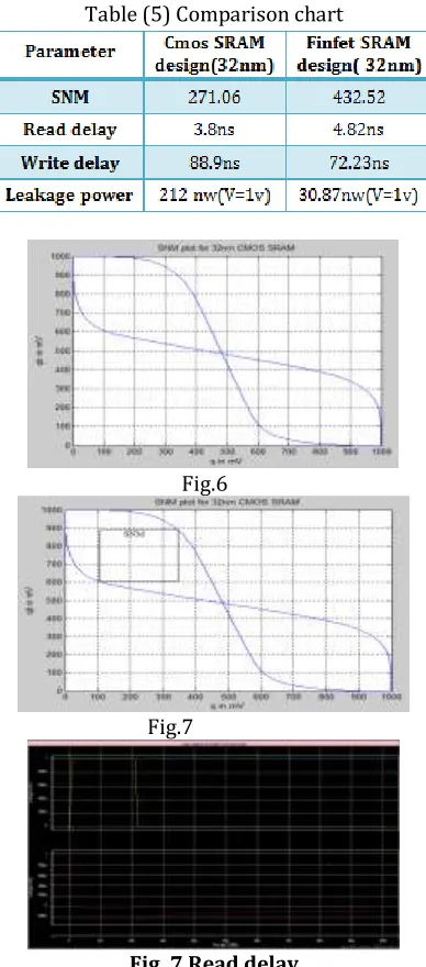
In 6T SRAM the objective is how to reduce the leakage power, delay, and increase derive current for SNM in comparison to CMOS design. The differences are seen in comparison table. The leakage power is reduced to almost one fourth in Finfet SRAM and the delay is slightly changed because of circuit design in both cases ,either 6T Finfet SRAM, or 6T CMOS SRAM. SNM value is also increased due to increasing the number of fins and thickness of fin.
Table (5) Comparison chart
Fig.6
Fig.7
Fig.8 Write delay
VI. CONCLUSION
In this paper the problem of short channel effect, power dissipation, leakage power is reduced due to use of Finfet device. It increases the chip area and transistor density by using Fin like structure. In this paper we perform the Finfet device simulation on TCAD ,variation of parameters is done and the optimized result is calculated regarding derive current of Finfet .6T SRAM circuit is also designed to find the optimized result of SNM, delay ,leakage power which can make the circuit efficient in their working.
REFERENCES
[1]. Balwinder raj, A. K sexena “Nano scale FINFET
based SRAM cell design: Analysis of performance matrix, process variation, Underlapped finfet and Temperature effect. IEEE Circuit and System magazine, pp 39 -50. SEPTEMBER 2011.
[2]. Nidhi sharma “A novel technique of leakage
power reduction in 9T SRAM design in FinFET
technology”IEEE,2016 6TH International
conference ,pp 737-743, july 2016 .
[3]. Alexandra L. Zimpeck “FinFET Cells with Different
Transistor Sizing Techniques against PVT Variations” IEEE ,2016 International symposium ,PP 43- 47, 11 AUG 2016.
[4]. Venkata P. Yanambaka “Process Variation
Analysis and Optimization of a FinFET based VCO” Volume 30 Issue 2, IEEE Transactions on Semiconductor Manufacturing, pp 2-8,MAY 2017.
[5]. Ramachandran Muralidhar “A Comparison of
Short-Channel Control in Planar Bulk and Fully Depleted
[6]. Devices”, IEEE Electron Device Letters, VOL. 33,
NO. 6, pp 776-778, JUNE 2012.
[7]. Zhichao Lu and Jerry G “Short-Channel Effects in
![Fig 1 structure of Intel’s tri-gate FinFET [6]](https://thumb-us.123doks.com/thumbv2/123dok_us/8795897.1769200/1.612.326.530.283.419/fig-structure-of-intel-tri-gate-finfet.webp)