Copyright © 2012 IJECCE, All right reserved
Implementation of Fast Pipelined Data Encryption
Algorithm (DES) Architecture with Scan Based Side
Channel Attack
S. Sudha Rani
Department of ECE DVR & Dr. HS MIC College of Technology, Kanchikacherla, AndhraPradesh, India-521180
Triveni. B
Department of ECE Vijaya Institute of Technology for Women, Enikepadu, Vijayawada, AndhraPradesh, India–521108
S. Umamaheshwar
Department of ECE Balaji institute of Technology and Science, Narsampet, Warangal, AndhraPradesh, India- 506331
Abstract – The primary objective of this work was to implement an innovative architecture that computes the basic Data Encryption Standard (DES), which is used in a wide range of communication systems to protect information being transmitted over a channel from being intercepted and read by unauthorized parties. DES is probably one of the best known cryptographic algorithms, and has been widely used. Compared to software implementations, hardware implementations of the DES algorithm provide more physical security as well as higher speed. As compared to the existing DES implementations in the present design, this work targets at a higher operating frequency, higher throughput by enhancing on the lines of pipelining concept. The pipelined structure minimizes the computation time overhead by key and message loading. The DES mode of operation is considered is the basic Electronic Code Book (ECB). Further the utility of scan chains is used as a side channel attack to recover the secret key from the hardware implementation of the DES. Scan chains are used to discover the secret key stored in the cryptographic devices. The round keys are recovered using certain mathematical assumptions, on the scanned out bits. The hardware architecture is described using Verilog HDL and is simulated to test its functionality.
Keywords – Data Encryption Algorithm, Electronic Code Book, Side Channel Attack.
I. I
NTRODUCTIONThe rapidly increasing demands for using internet and wireless communication have led to the development of efficient security algorithm and devices to protect the transmitted information over open channels. In Oct. 1999, the Data Encryption Standard (DES) [1-3] was selected by the National Institutes of Standards and Technology (NIST) as an encryption standard. Most of the information in today’s world is in digital format. For example most of the information in the form of photos, music and private information can be transmitted through copper, optical or wireless network to a recipient anywhere in the world. In order to protect the data and keep privacy, the information system should be equipped with cryptography and robustness techniques (4, 5).The present study proposes the design of Data Encryption Standard (DES) crypto-processor using basic Electronic Code Book (ECB) mode of operation. The design is pipelined to accelerate fast computation of digital data encryption and decryption using pipelined DES algorithm in order to increase operating frequency and throughput.
Objectives
1. To develop Straightforward DES architecture. 2. To pipeline the above straightforward architecture
along the critical path so as to increase the frequency of operation.
3. To insert scan chain, to demonstrate the scan based side channel attack.
Literature Survey
Encryption and decryption are the two main functions in cryptography system. Encryption is the transformation of data into a form unreadable by anyone without secret key in order to ensure privacy. The information is hidden from anyone for whom it is not intended, even from those who can see the encrypted data. Encryption also allows secure communication over an insecure channel especially Internet. Decryption is the reverse function to retrieve the original encrypted messages using secret key.
Study of various available architecture
Key to small silicon area and high performance is a chip architecture carefully optimized by use of an optimized design strategy.DES begin a standard encryption algorithm is implemented using various architectures. The architecture selection makes a tradeoff between parameters such as speed, operating frequency, power, and throughput. All of this architecture describes the way in which the data is processed. motivated on the lines of scalable computing, an architecture is described [6], where the basic replicated unit is a triad of nodes optimized for number of computation and device access respectively, with an interposed bridge node comprising a bus bridge and embedded control processor the bus bridge serves as a hardware security barrier between the computational node, which does not need to operate on the content of the data blocks it manages and moves around the other architecture evolve around the concept of XOR MAC [6-7] which is the widely used cryptographic message authentication code (MACs) which is amenable to pipelined and parallel implementation.
Copyright © 2012 IJECCE, All right reserved several types of environments a general flexible IO
interface has to be provided. Drawbacks with most of the architecture are that, they cannot be used for all modes of operation.
II. D
ESIGNM
ETHODOLOGIESStraight Forward System Design
This section describes the two architectures straightforward, pipelined and the methodologies involved in their design. Ironically the control is independent of the data in the DES algorithm. The figure below describes the architecture used in the project to implement the basic DES algorithm.
Fig.1. Straightforward DES architecture
Processing operation is first initialized by shuffling of bits. The more the diffusion and confusion the tougher it is to crack the key. The bits are shuffled first based on a look-up table, put forward by NIST [1].Known formally as the initial permutation IP, the Feistel scheme terminates with de-shuffling or inverse permutation FP (final permutation). FP=IP-1.As in here, since data is only encrypted , the key bits are void off the parity bits which is used only in case of authentification. Like in case of the message bits, the key is also shuffled in a similar way based on PC1.The round logic modifies the key bits each round. This transformation termed as key schedule, consisting of defined number of Left shifts or Right shifts (LS, RS), resulting in encipherment, decipherment respectively, depending on PC2.The bit shuffling primitive that constitutes the DES design include permutations, multiplexers and flip-flop. A 4 X 1 mux chooses one of the below mentioned operations.
1. Concatenation 2. Starting Computation
3. Reinjecting data for the next round 4. Swapping operation
In the straightforward scheme, every computation has an overhead in execution time due to data loading/unloading in the LR or in CD register. The evaluation of the architecture throughput does not take into account the key loading, because most applications use only one key, loaded once for many consecutive cipherments.
III. P
IPELINES
YSTEMD
ESIGNGiven below is the flow chart that depicts the flow of control in a pipelined architecture. The refinements carried out on the above mentioned straightforward architecture, because they are “pipelined”: data (other than key) flows continuously through the data path, without having to wait at any time.
Fig.2. Pipeline DES Flow-Chart
Speed Up Due To Pipelining
The straightforward architecture suffers two drawbacks that impede the crypto processor performances:
(1) The DES cannot perform cipherment while new blocks mi +1are read and processed blocks DES (mi)
are written out.
(2) The LR register is preceded by multiplexers that increase the critical path.
Critical path delay is given by tcomb..The delay of the
critical path tcomb, through the combinational logic limits
the minimum clock period Tflip-flop, as given below.
Tflip-flop= maxi{tcomb} + tregister + tclocking ---- (1)
Pipelining Latency is the time from the arrival of the pipeline inputs to the pipeline, to the exit of the pipeline outputs corresponding to this given set of inputs, after calculation in the pipeline. There is only a single stage in pipeline so the path TLatencyis simply the clock period.
TLatency =tcomb+ tregister+ tclocking --- (2)
Supposed this logic path is pipelined into “n” stages of combinational logic between registers as shown below,
Fig.3. Pipelining in order to reduce the critical path
Copyright © 2012 IJECCE, All right reserved
Architecture Description
The pipelining is achieved by the use of intermediate register, known as the interface register or the IF registers. It holds the data, to be concatenated after the required number of clock cycles.
Pipelining Operating Principle
The figure given below shows the pipelined DES architecture 64-bit is fed as an input and stored into the register IP, the procedure being the same as in the case of straightforward. The inputs will be encrypted in the architecture simultaneously. The first encrypted output will be produced at the 16thround, second at the 17thround and so on and so forth.
Fig.4. Pipelined Architecture.
Pipeline architecture gives one block of cipher (64 bits) every clock cycle, except at the beginning when pipeline need to be filled (during 16 clock cycles because we have 16 stages), so there is a latency of 16 clock cycles. Pipelining tries to achieve speed improvement in a different way .Instead of processing one block of data at a time, a pipeline design can process two or more data blocks simultaneously. The drawbacks put forward in the previous section can be overcome by a pipelining scheme of the DES crypto processor. The difference is that a straightforward DES engine can process one cipherment at the time, whereas a pipeline DES engine processes many—up to 16 – at the same time. Pipeline in general refers to the way in which data is loaded and unloaded. In case of pipelined architecture a 64-bit register, called IF (Interface register) is used. It is so called because of its interface between the 8-bit inputs and the 64-bit blocks involved within DES.
IV. S
CANC
HAINI
NSERTION ANDS
IDE-C
HANNELA
TTACKFig.5. Scan based attack
Usage of scan in cryptographic chip decreases the security level. Scan chains used to discover the secret key stored in the cryptographic devices. Pairs of plaintexts with a bit difference are loaded in normal mode, and their internal states are scanned out in the test mode. The scan elements position is determined. The structure of non-linear substitution boxes along with three additional plaintexts are analyzed to discover the secrete key [3]. DFT provides high fault coverage without the requirement of additional hardware for test pattern generation. One of the most powerful and widely used scan based test.
Registers and flip-flops are tied together to form scan chains.TCK and TMS stand for test clock select and test mode select signals. Scan D flip-flops replace the original D flip-flop in the scan chain. In test mode the content can be scanned in and out. In chip packaging all scan chains are connected to JTAG external boundary pins.
Scan Chain Determination
Fig.6. Scan chain determination
In order to locate the position of L and R registers in scan chain the following process is done.DES is made to run in normal mode for one clock cycle to load the plain text into the input register. The bit pattern is then scanned out in test mode (pattern 1). Again it is made to run in normal mode and run for one clock cycle, and bits scanned out (pattern 2). The above procedure is repeated again but with plain texts that differs from the original in one bit position, thereby giving pattern 3 and pattern 4 respectively.
While observing pattern 1 and pattern 3 there is seen a one bit difference, which determines the location of input register flip-flop. Similarly a two-bit difference is observed from pattern 2 and pattern 4.This difference is due to one from input register and other from L or R registers.
Round Key Recovery
On knowing the position of Land R registers in the scan chain, DES algorithm can be broken by applying three known plaintext and analyzing the following mathematical relations.
L1= R0 (4.1)
R1= L0 ^d (4.2)
d = permutation (C) (4.3)
a = expand (r) (4.4)
b = a ^ k1 (4.5)
Copyright © 2012 IJECCE, All right reserved In the above set of equations all except ‘b’ value can be
obtained. In order to obtain ‘b’ value, i.e. the input to the S-boxes from their output C. For instance the structure of a s-box, S1, S2……..S8 is given below.
Fig.7. S Box Structure S1
Assume 6 most significant bits are the inputs to the S-box {b48 b47 b46b45b44b43}. b48and b43denotes the row
number, and b47 ……b44 denotes the column number. As an example consider the sequence given b48b47b46b45b44b43
= (011011).The row is 01 and column is determined by 1101, that is the 13th column. In row 1 and column 13 appears 5.Hence the output is 0101.An S-box compresses the 6-bit input into 4-bit output. Every output value appears exactly four times. For instance in the above Example of S_box S1.For instance in the above example of S box S1, the value 8 appears in the following locations (0,7) (1,15) (2,3) (3,2).If the output of S_box is 8 then { b48 b47 b46 b45b44b43} can be any one of the following
values, (001110)2 , (011111)2 , (100110)2 or (100101)2.
Observing just one value does not determine the input to the S-box since the value appears four times. A minimum of 3 values must be applied in order to uniquely determine the round key from the observed outputs at C. Following mathematical analysis proves handy in obtaining the value at a point C.
V. R
ESULTS ANDA
NALYSISAs the transistor feature size is scaled down, more and more functionality can be integrated in a single chip. High speed, high complexity, and short design time are several requirements for VLSI designs. This requires that the design methodology must cope with the increasing complexity using a systematic approach. A design methodology is the overall strategy to organize and solve the design tasks at the different steps of the design process. In the top-down design methodology, the system requirements and organization is developed by a successive decomposition. Typically, a high-level design language is used to define the system functionality. After a number of decomposition steps, the system is described by a HDL, which can be used for automatic logic synthesis & optimization. Furthermore, a system-level verification environment ensures that system requirements are met and provides the infrastructure for verifying the subsystems and system components. The top-down design approach results in higher confidence that the completed design will meet the original schedule and system specifications. Hence, this project uses the top-down design methodology for implementation.
Analysis of simulation results of straightforward
pipelined and scan based DES architectures
Few important parameters are obtained from waveform simulation, which are:
i. Clock cycle ii. Time taken iii. Throughput
Clock cycle is the total number of clock cycle taken to complete the design simulation. Time taken is the overall time for the design to produce a correct output. Throughput is the number of bits that can be processed by the design within a time of one second. These three parameters depend on the targeted hardware and the supported frequency for the hardware. Normally, clock cycle is counted from the moment of the circuit starts to process the initial data or input until it can produced the final desired output or results.
The DES architectures (straightforward & pipeline) have been described using Verilog HDL, and simulated using Cadence ncsim.
Des_input: (plain text)
55579380_D77138EF Initial Key:
00000_00000000 Des_out: (cipher text)
04000000_00000000
Straight forward Architecture
Fig.8. Simulation of straight forward DES
Pipelined DES Architecture
Fig.9. Simulation of pipeline DES
Copyright © 2012 IJECCE, All right reserved When analyzing the pipelined simulation result it
clearing seen that the pipeline stage is busy during the 16 clock cycles, in order to load the key and message bits in CD register, after which output is obtained after every subsequent clock cycle thereby increasing throughput.
Simulation of Scan Based Side Channel Attack
To demonstrate how scan chains can be used as a side channel to recover secret keys from a hardware implementation of the Data Encryption Standard (DES).Scan chains can be used to discover the secret keys stored in a cryptographic device. Based on some assumptions and systematic analysis of the structure of the non-linear substitution boxes, we discover the DES secret key. The primary objective of RTL scan insertion is to reduce the time taken for DFT, & thus reduce the time to market. Building scan chain at the functional RT-Level is expected to reduce the total area overhead introduced by full scan without compromising the fault coverage achieved. It eliminates the delay associated with the additional multiplexers as a part of a conventional scan-chain in high performance designs.
Logic Used
During test synthesis, a D flip-flop is replaced with its equivalent scan D flip-flop when it is included in a scan chain. A scan D flip-flop is a D flip-flop with a MUX at the D input. In normal mode (input 0) it works like a D flip-flop, in test mode it’s contents can be scanned in and out. All scanned flip-flops are disconnected from the combinational circuit and connected to each other in scan chain. Compared to BIST (built in self test) scan based test provide high fault coverage and do not need hardware for test pattern generation and signature analysis.
Fig.10. Scan Simulation Result
Applying the above steps mentioned in chapter 4 and by applying the equations given above we get the round key for the 1stround as 1061B8_18D1CEA5, which is same as the one got through simulation. This when iterated according to the algorithm specification breaks the cipher text and obtains the plain text.
Functional Verification Results
From functional simulation, the design correctness as expected is verified. Starting from the smallest modules in the lowest hierarchy of the hardware component, waveform simulations are performed for all the modules in the hardware design. Test vectors are used for this purpose.
Fig.11. Functional verification of pipeline DES
Implementation Results
Given below is the implementation result between STRAIGHTFORWARD and PIPELINED architectures.
Architecture Straight
Forward Pipelined
Technology 0.18um CMOS 0.18um
CMOS No. of Routing
Layers 6 6
Total area of Core 27509.3 um^2 315608.8
um^2
Power Supply 0.9v 0.9v
Operating
Frequency 660 MHz 800MHz
Avg. Power
dissipation 12.2269mW 82.526mW
Throughput 2 4
Table 1: Design budgets of straightforward & pipelined architecture
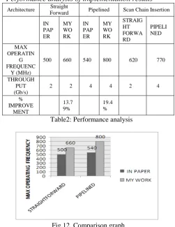
Performance analysis of implementation results
Architecture Straight
Forward Pipelined Scan Chain Insertion
IN PAP ER
MY WO RK
IN PAP ER
MY WO RK
STRAIG HT FORWA RD
PIPELI NED
MAX OPERATIN
G FREQUENC
Y (MHz)
500 660 540 800 620 770
THROUGH PUT (Gb/s)
2 2 4 4 2 4
% IMPROVE
MENT
13.7 9%
19.4 %
Table2: Performance analysis
Copyright © 2012 IJECCE, All right reserved The above graph portrays the comparison between the
maximum operating frequency and throughput of the existing work and the results obtained. As known pipelining increases the operating frequency as well as the area (instance count).The area increase is due to the insertion of additional registers. In a typical pipelined design the clock tree may be responsible for 20% to 45 % of the total chip power consumption. Turning off the clock that is Clock gating to modules that are not in use reduces the clock power. As seen there exists a tradeoff between area and operating frequency. This architecture avoids the usage of RAM, thereby improving the operating frequency. The exiting architecture uses RAM for data loading at the input stage which increases the area overhead.
VI. C
ONCLUSION ANDF
UTURES
COPEThe DES architecture has been implemented and pipelined in order to increase the operating frequency. The proposed design methodologies exhibit a tradeoff between speed and area. It has been found that straightforward architecture is the most compact compared to pipeline, where as pipelined architecture has a higher throughput and operating frequency compared to straightforward. The area increase in case of pipelining is due to the addition of pipelining registers. The designed architecture can be adapted to an external data path of width n=16 or n=32.The exiting architecture uses RAM for data loading at the input stage which increases the area overhead. This architecture avoids the usage of RAM, this proves to be advantageous as RAM has limits over maximum operating frequency, in order to operate without violating either hold or setup time constraints.This can be further enhanced by including the other block cipher modes of operation such as OFB and CFB. A higher throughput can also be achieved by parallel processing the architecture. Another desired utility of authentification can be added by including the XOR Mac design as a future work.
R
EFERENCES[1] Joan Daemen and Vincent Rijmen, AES submission document on Rijndael, June 1998.
http://csrc.nist.gov/CryptoToolkit/des/rijndael/Rijndael.pdf [2] Data Encryption Standard (DES). Federal Information
Processing standards publication. 1999 October 25. http://csrc.nist.gov/publications/fips/fips46/fips-46.pdf
[3] Sylvain Guilley, Phillippe Hoogvorst, Renaud Pacalet. A fast pipelined multi-mode DES architecture operating in IP representation. Integration, the VLSI Journal, 2007: 40 (4), 479– 489.
[4] Fakariah Hani Mohd Ali, Ramlan Mahmod, Mohammad Rushdan and Ismail Abdullah. A Faster Version of Rijndael Cryptographic Algorithm Using Cyclic Shift and Bit Wise Operations. International Journal of Cryptology Research 1(2): 215-223 (2009)
[5] Ming-Haw Jing, Yan-Haw Chen, Zih-Heng Chen, Jian-Hong Chen and Yaotsu Chang (2010). Design of Simple and High Speed Scheme to Protect Mass Storages, Data Storage, Florin Balasa (Ed.), ISBN: 978-953-307- 063-6, InTech, Available from: http://www.intechopen.com/books/data-storage/design-of-simple-and-highspeed-scheme-to-protect-mass-storages
[6] X. Zhang and K. K. Parhi, “Implementation approaches for the advanced encryption standard algorithm,” IEEE Circuits Syst. Mag., vol. 2, no. 1, pp. 24–46, Jan. 2002.
[7] H. Kuo and I. Verbauwhede, “The data encryption standard : past and future,” in Proc. Cryptograph. Hardware Embedded Syst., Paris, France, May 2001, pp. 51–64.
[8] Bo Yung, Kaijie Wu, “Scan based side channel attack on data encryption standard,” in Proc. Cryptograph. Hardware Embedded Syst., Paris, France, May 2001, pp. 77–92.
[9] Peter R.Wilson and Andrew D. Brown, “DES in four days using behavioral modeling & synthesis ,”IEEE Trans. Comput., vol. 51, no. 12, pp. 1454–1459, Dec. 2002.
A
UTHOR’
SP
ROFILES. Sudha Rani
Received M.Tech degree in Digital Systems and Computer Electronics from Jawaharlal Nehru Technological University, Hyderabad in 2010 and received B.E degree in Electronics and Communication Engineering from Sir C. R. Reddy college of Engineering, Eluru in 2007. Currently, she is working as an Assistant Professor in DVR & Dr. HS MIC College of Technology, Kanchikacherla, Andhra Pradesh. Her area of interest is Digital Signal processing, VHDL, Digital Communications.