www.adv-radio-sci.net/14/121/2016/ doi:10.5194/ars-14-121-2016
© Author(s) 2016. CC Attribution 3.0 License.
PCB current identification based on near-field measurements using
preconditioning and regularization
Denis Rinas, Patrick Ahl, and Stephan Frei
AG Bordsysteme, TU Dortmund University, Dortmund, 44227, Germany Correspondence to:Denis Rinas ([email protected])
Received: 14 January 2016 – Revised: 11 June 2016 – Accepted: 21 June 2016 – Published: 28 September 2016
Abstract. Radiated electromagnetic fields from a PCB can be estimated when the source current distribution is known. From a measured near-field distribution, the PCB source cur-rent distribution can be found. Accuracy depends on the mea-surement method and its limitations, the radiation model and the choice of the observation area. Many known methods are based on optimization algorithms for inverse problems that vary a set of elementary radiation sources and create a radi-ation model. However, apart from the time-consuming opti-mization process, such methods find one possible solution for a near-field distribution. As this distribution might not reflect the real current distribution, accuracy outside of near-field scan area can be low. Furthermore numerical problems can often be observed. Solving the given inverse problem with a system of linear equations and complex near-field data it can be very sensitive to noise. Regularization methods and an ad-justed preconditioning can increase the accuracy. In this pa-per, an improved radiation model creation approach based on complex near-field data is presented. This approach is based on regularization methods and extended by current estima-tions from near-field data. Preconditioning is done consid-ering some physical properties of the PCB and its possible current paths. Accuracy and stability of the method are in-vestigated in the presence of noisy data.
1 Introduction
Alternative methods for evaluation of electromagnetic emis-sions from electronic components (e.g. near-field scan meth-ods) have several advantages against antenna measurement methods (e.g. ALSE method from CISPR 25, CISPR 25 Ed.3, 2007). Single field strength values obtained from an-tenna in transition- or far-field, cannot describe the
over-all emission behavior of a device under test (DUT). Repro-ducibility is often limited (Burghart et al., 2004) and iden-tification of radiating sources can be reached only for sim-ple structures (Nishikata et al., 2014), but obviously not in case of a complex device. The large space requirements and high costs of an antenna measurement environment have to be considered too.
Knowing the fields in an infinite plane above an object means, all information is available to calculate field above this plane (Balanis, 1996). From theoretical point of view this would be sufficient to calculate the far-fields of a printed cir-cuit board (PCB). But there are several problems with such a direct approach, e.g. it is not possible to measure field along an infinite plane, accuracy of measurements is limited and accuracy of near-field to far field transformation can be low. Furthermore obtaining far-fields is often not the only aim, also the identification of radiating and disturbing sources, as mentioned above might be needed. Knowing the sources, strategies for noise reduction can easily be developed. There-fore the inverse problem of the resulting electromagnetic field and the causing current distribution on PCB should be solved.
approxi-Figure 1. (a)PCB sources approximated by regular grid dipole model.(b)Spectrumi= [1, N]of singular values and condition numbersµi
for different scan heights and resolution.
mating currents is modified, until the measured near-field distribution of the radiating structure and its model agree. Naturally these approaches can also be applied to complex near-field measurement data. Although these methods of-ten achieve good results, at least in approximating the ref-erence observation plane, the underlying algorithms involve the problem of converging to local minima (Isernia et al., 1996). Besides they can result in a very long computation time. To improve model quality known physical properties of the radiating currents can be included in current distri-bution estimations. This way the number of free source pa-rameters (Rinas et al., 2011) and sensitivity to noise can be reduced. Resulting radiation pattern is more accurate outside the measured area or volume. Here the trace geometry is as-sumed to be known, from computer-aided design (CAD) – data or the near-field measurements, and the spatial distribu-tion of the possible current paths can be limited. Furthermore current phases are correlated to each other. These improve-ments lead to reduced computation time and increased accu-racy. The second type is the complex field data based model (Laurin et al., 2001; Xin et al., 2010b; Rinas et al., 2013). Here the sources are determined from both magnitude and phase information of the near-field data. Of course optimiza-tion algorithms can be applied here again but it is sufficient to solve a system of linear equations using complex data. The set of linear equations can be ill-conditioned and the solu-tion might be erroneous. Regularizasolu-tion techniques can be applied to deal with such problems, e.g. Tikhonov regular-ization (Xin et al., 2010b; Tichonov and Arsenin, 1977). Fur-thermore preconditioning of the linear map of the system can be done to create an optimal database for current identifica-tion.
In this paper an optimized method for current identifica-tion on PCBs based on solving a system of linear equaidentifica-tions containing regularization is introduced. Noise sensitivity for current identification process is compared to other methods and need of model preconditioning is shown. Possible cur-rent path locations are limited by the locations of the existing traces of the investigated PCBs. Thus there is a benefit due to the physical preconditioning but without the disadvantage of long computation time. This method leads to an equivalent
radiation model with good accuracy. Furthermore it can be applied to measurement data obtained with typical EMC test equipment (test receiver, spectrum analyzer) without phase information and therefore an extremely ill-conditioned prob-lem. Improvement of method stability is shown by noise analysis and application to real measurement data.
2 Current identification method
To identify currents complex horizontal magnetic near field componentsHxandHyin a plane above radiating structure are used. As standard and most simple model structure at first equivalent sources are arranged in a grid with resolution1dq above an infinite ground plane (Fig. 1a). Each source con-sists of a triple of electric dipoles, where each dipole rep-resents a current direction in Cartesian coordinates. The in-verse problem between field data and dipole current is solved mathematically with a least squares system and use of pseu-doinverse. Following the uniqueness theorem the solution of the inverse problem should produce a good image of the real sources, if the field in a surface around a radiating structure is known. In such a theoretical configuration solving the sys-tem of linear equations will create an accurate model with an equivalent current distribution. Obviously the measurement accuracy and size of plane are limited. The radiation model might not be perfect. As result field data will be erroneous or noisy.
2.1 Noise sensitivity in current identification process
by
id(t )= ∞ X
i=1 (ui, h)
µi
vi(t ) (1)
Where id stands for the currents to be identified, h is the known field distribution, ui and vi stand for the singular functions of the Fredholm kernel andµi for its singular val-ues. Sincehis decomposed to its spectrum it is obvious from Eq. (1) that a small singular value µi will strongly amplify the corresponding spectral part ofh. This means noise, lo-cated in the higher frequency region, will be amplified in case of a large spectral condition number (Hanson et al., 1971). In our investigations we used the magnetic field as the known right-hand side values. The currents are reproduced by ele-mentary Hertzian dipoles. The system of linear equations in this case is
H(r1) .. . H(rM)
| {z }
H
=
9r1,rQ1 · · · 9r1,rQN
..
. . .. ...
9rM,rQ1 · · · 9rM,rQN
| {z }
9
×
IQ1 .. . IQN
| {z } I
(2)
Where vectorH contains the knownH-field values, vector
I contains the unknown currents and the matrix9is the lin-ear map containing the geometry and wave propagation. If no further information about sources is available they can be placed for PCBs in form of a regular grid with resolution1dq (Fig. 1a).
To create an accurate radiation model of a PCB the pre-conditioning of the inverse problems linear map must avoid a high condition number and must allow a wide frequency range. The spectral requirements of the singular values nat-urally depend on the given structure of the PCB, so that in a strongly restricted singular value spectrum the traces can-not be reproduced accurately. Figure 1b shows exemplary the condition numbers and frequency ranges for different near-field scan linear maps based on simulation data. It can be seen, that for a high scan resolution and high scan height the linear map is bad conditioned. Due to the high number of dipoles the spectrum is wide and the small singular val-ues in high frequencies will strongly amplify the noise (case 1). Whereas in case of a low scan resolution and low scan height the linear map is well conditioned. The low number of dipoles results in a low spectral range (case 2). Of course, the condition number depends on the relation between num-ber of scan points and position of scan points to numnum-ber of dipoles and position of dipoles. It is not sufficient to reduce scan resolution and scan height and to increase the number of dipoles. Not only that a low number of scan points and a
high number of dipoles can cause an under-determined sys-tem of equations, but also prevention of undersampling must be ensured (Yaghijan, 1986), following
1ds< λ/
2 q
1+(λ/hs)2
(3) Whereλis the wavelength of the highest frequency,hsis the height of the scan plane and1dsstands for the minimal scan resolution.
2.2 Current estimation of PCB traces using near-field scan data
Obviously it is not possible to find the best preconditioned linear map for each near-field scan problem. Here regular-ization methods (e.g. Tikhonov method) can be applied to smoothen the linear system and to generate a less noise sen-sitive and more accurate model (Xin et al., 2010b; Hanson, 1971). The problem is here given by
minnkAx−bk2
2+λtkL(x−x0)k22 o
(4) Where the parameterλt describes the regularization param-eter andLis a regularization matrix, which can be adapted. In a general approach, theLmatrix is chosen as the identity matrix andx0is set to zero. This can be done when no par-ticular knowledge is available. In Zhenwei et al. (2010) theL matrix values are extended by a frequency dependency, but without a current estimation forx0.
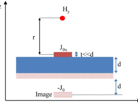
In case of a planar near-field scan above a simple PCB on a ground plane a current estimation from near-field scan can be done. For a single trace, with an assumed infinite length, the current can be approximately calculated from the magnetic field above this trace using image theory (Fig. 2) (IEC/TS 61967-6 Ed.1.0, 2002):
I0x=Hy
π r (r+2d)
d (5)
With decomposition ofHxandHy the current from each trace can be estimated. For high accuracy a sufficiently high scan resolution and low scan height is required. The esti-mated current amplitudes are implemented in the regulariza-tion method and provide an improved convergence to the real current. The problem for the PCB current identification is now given by
minnk9J−Hk22+λtkIn(I−I0)k22 o
(6) Here the regularization parameterλt contains the Wiener fil-ter as proposed in Hanson (1971) andInis the identity ma-trix.
2.3 Current path identification
Figure 2.Current estimation from magnetic field of a PCB-trace above ground plane using image theory.
infinite ground plane. As proposed in Sect. 2.2 the ampli-tude for each current path section can be estimated from the magnetic near-field data. Furthermore this estimation can be used for preconditioning the linear map of the system of lin-ear equations. In a first step the matrix9 can be reduced by eliminating the entries from dipoles with a current estimation much smaller than the maximum in its neighborhood. This relation depends on the given signal-to-noise ratio (SNR) and the model resolution.
9n,m=
0 if9n,m<max 9n±1n,m±1m−(SNR+s)
9n,melse (7)
Where the indexn+1nandm+1mdescribe the neighbor-hood and s is a threshold value to be defined. In a second step the orientation of the current path can be used to reduce the dipole triple at each grid point to its decomposed parts following the estimated current path.
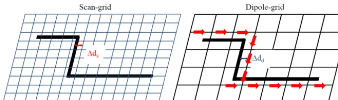
Obviously, arrangement of PCB current paths into a reg-ular grid leads to discretization errors (Fig. 3). The approx-imating dipole path is shifted by1ddfrom the real current path, depending on the grid resolution. Additionally the un-avoidable discretization errors of the scan grid against the dipole positions1ds, will influence the current estimation. Therefore interpolation methods are applied to achieve the field vectors above each equivalent current. The sum of these discretization errors will influence the results, particularly strong if the solution method has to deal with such kind of ill-conditioned problem.
To create an accurate model, as we mentioned in Rinas et al. (2011), the current paths of a PCB can be achieved from CAD-data of the board, computer tomography or with a high-resolution pre-near-field scan. This means the equiva-lent currents can be distributed along the known traces. Thus the dipole path shift discretization errors are negligible, the
size of the linear map can be reduced and the model becomes more physically.
3 Results
In the following section results of the proposed current iden-tification method are presented. It is validated with ideal sim-ulation data first, second with noisy simsim-ulation data and later it is applied to real measurement data of a simple test PCB. It consists of a single trace which is fed by an AC voltage source in simulation and a 4 MHz trapezoidal signal in the real setup. The termination is a 100resistor. Geometry and configuration of the test PCB are shown in Fig. 4a and b. 3.1 Simulation data based results
3.1.1 Ideal data
The magnetic near-field above the test PCB is achieved in a 160 mm×100 mm plane 8.5 mm above ground. The reso-lution is set to 3.5 mm. Three different models are consid-ered: Model 1, a dipole grid distribution with fixed grid size (5 mm), without current estimation, solved by least squares method (LSQ); Model 2, a dipole grid distribution with fixed grid size (5 mm) with current path identification (CPI) solved by regularization method (Reg.); Model 3, a dipole distribu-tion along the real current paths (5 mm), with current estima-tion, solved by regularization method.
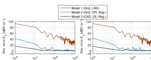
Figure 5 shows the current amplitude relative errors and phase absolute errors at the specific trace coordinates at a frequency of 100 MHz. Figure 6 presents the electric fields at an observation point P about 1.5 m far away from the PCB in a frequency range from 1 MHz to 1 GHz. This observation point represents a possible measurement antenna position. It can be seen that the field in horizontal and vertical position is quite accurate for all models from a frequency of about 50 MHz to 1 GHz. Below 50 MHz there is a significant de-viation for the simple grid model with LSQ method. A good accuracy for current identification in amplitude and phase is only reached by CAD-data based model with regularization. Especially model 1 shows unphysical jumps in current ampli-tude and phase. At 100 MHz it can be seen, although current distribution does not match the desired and physically cor-rect current, the field is approximated well. When only the field is required for accurate data it seems to be sufficient to find an arbitrary current distribution, which approximates the field in the reference plane.
3.1.2 Noisy data
In a next step noise is added to the ideal simulated magnetic near-field. A SNR of 10 dB is assumed. The same models (Model 1–3) are applied for current identification.
Figure 3.Discretization errors; error in scan plane discretization (left); error in dipole grid discretization (right).
Figure 4. (a)Configuration of test PCB.(b)Picture of PCB scanning.
Figure 5.Relative error of current amplitudes (left) and absolute phase error (right) of different models at given trace coordinates (100 MHz).
Figure 6.Horizontal (left) and vertical (right) electric field absolute error at observation point P.
Figure 7.Relative error of current amplitudes (left) and absolute phase error (right) of different models at given trace coordinates (100 MHz).
Figure 8.Vertical magnetic near-fields in observation plane com-pared to the simulated near-field (100 MHz).
Figure 9.Horizontal (left) and vertical (right) electric field absolute error at observation point P.
is particularly obvious for model 1 which shows current am-plitude and phase jumps. For noisy data it is not enough to approximate the field in reference plane to create an accurate model. In Fig. 8 can be seen that regularization and CAD-data filter noise and produce a smoothed near field which matches the near field of the undisturbed PCB. This leads to a stable and accurate current and field calculation model. 3.2 Measurement data based results
The magnetic field distribution of test PCB is now given by Time Domain measurements (Rinas et al., 2011) with a pas-sive magnetic field probe with 3 mm loop diameter connected to an oscilloscope. The complex field data is transformed into Frequency Domain with FFT and a reference signal for phase calculation was used. The measurement plane of 160 mm×100 mm was located 4.5 mm above ground.
Figure 10 shows the errors of identified currents for model approach 1 and 3. It can be seen, that the accuracy of the results is improved significantly when using real PCB current trace locations and regularization method.
4 Conclusions
Current distribution based radiation models from near field scan data for evaluating the electromagnetic field from PCBs need precise field data for current estimation. As measure-ment with very high accuracy are often impossible, pro-posed approaches try to identify the currents using
optimiza-Figure 10.Relative error of current amplitudes (left) and absolute phase error (right) of different models at given trace coordinates (100 MHz).
tion algorithms (e.g. amplitude-only data). Thereby the loca-tion, amplitudes and phases can be varied, until one or more desired near-field planes are approximated. Although these methods often find a very good solution for their reference plane, accuracy outside of near-field scan area can be low. Solving the inverse problem with a system of linear equa-tions and complex near-field data can be very sensitive to noise. Regularization methods and an adjusted precondition-ing can increase the accuracy. Furthermore, the possible cur-rent paths can be restricted to the physical curcur-rent paths on a PCB. This can be done by CAD-data, computer tomogra-phy, or with a high-resolution pre-near-field scan. Addition-ally the current amplitudes can be estimated from the near-field data. These precondition measures were implemented for more accurate identification of currents. The benefit and stability of the method was investigated by simulation and measurements with a simple test PCB. The results show an obvious increase of the model accuracy, in the identified cur-rents, and a good error correction in the case of a noisy ref-erence near-field.
5 Data availability
Part of this research was done within cooperation projects and is subject to individual confidentiality agreements. Data used for this publication cannot be disclosed.
Edited by: F. Gronwald
Reviewed by: two anonymous referees
References
Balanis, C. A.: Antenna Theory Analysis & Design, Wiley, 1996. Burghart, T., Rossmanith, H., and Schubert, G.: Evaluating the
RF-emissions of automotive cable harness, International Sympo-sium on Electromagnetic Compatibility, EMC 2004, 3, 787–791, 2004.
Hanson, R. J.: A Numerical Method for Solving Fredholm Integral Equations of the First Kind Using Singular Values, SIAM J. Nu-mer. Anal., 8, 616–622, 1971.
IEC/TS 61967-6 Ed.1.0: Integrated circuits, Measurement of elec-tromagnetic emissions, 150 kHz to 1 GHz – Part 6: Measurement of conducted emission, magnetic probe method, 2002.
Isernia, T., Leone, G., and Pierri, R.: Radiation pattern evaluation from near-field intensities on planes, IEEE T. Antenn. Propag., 44, 701–710, 1996.
Laurin, J., Zürcher, J. F., and Gardiol, F. E.: Near-field diagnostics of small printed antennas using the equivalent magnetic current approach, IEEE T. Antenn. Propag., 49, 814–828, 2001. Nishikata, A., Wada, Y., Tawada, M., and Takabe, Y.:
Three-dimensional dipole source identification using two fixed receiv-ing antennas and its new algorithm, International Symposium on Electromagnetic Compatibility, EMC Tokyo 2014, 33–36, 2014. Pierri, R., D’Elia, G., and Soldovieri, F.: A two probes scanning phaseless near-field far-field transformation technique, IEEE T. Antenn. Propag., 47, 792–802, 1999.
Regué, J.-R., Ribó, M., Garell, J.-M., and Martin, A.: A Genetic Algorithm Based Method for Source Identification and Far-Field Radiated Emissions Prediction From Near-Field Measurements for PCB Characterization, IEEE T. Electromagn C., 43, 520–530, 2001.
Rinas, D., Niedzwiedz, S., Jia, J., and Frei, S.: Optimization meth-ods for equivalent source identification and electromagnetic model creation based on near-field measurements, EMC Europe 2011, 298–303, 2011.
Rinas, D., Zeichner, A., and Frei, S.: Measurement environment influence compensation to reproduce anechoic chamber mea-surements with near-field scanning, International Symposium on Electromagnetic Compatibility, S. 705–710, 2013.
Sijher, T. S. and Kishk, A. A.: Antenna modeling by infinitesimal dipoles using genetic algorithms, Progress In Electromagnetics, 225–254, 2005.
Tichonov, A. N. and Arsenin, V. J.: Solutions of ill-posed problems, Washington, DC, Winston (A Halsted Press book), 1977. Xin, T., Thomas, D. W. P., Nothofer, A., Sewell, P., and
Christopou-los, C.: A genetic algorithm based method for modeling equiva-lent emission sources of printed circuits from near-field measure-ments, Asia-Pacific Symposium on Electromagnetic Compatibil-ity, 293–296, 2010a.
Xin, T., Thomas, D. W. P., Nothofer, A., Sewell, P., and Christopou-los, C.: Modeling Electromagnetic Emissions From Printed Cir-cuit Boards in Closed Environments Using Equivalent Dipoles, IEEE T. Electromagn. C., 52, 462–470, 2010b.
Yaccarino, R. G. and Samii, Y. R.: Phase-less bi-polar planar near-field measurements and diagnostics of array antennas, IEEE T. Antenn. Propag., 47, 574–583, 1999.
Yaghjian, A. D.: An overview of near-field antenna measurements, IEEE T. Antenn. Propag., 34, 30–4, 1986.
![Figure 1. (a) PCB sources approximated by regular grid dipole model. (b) Spectrum i = [1,N] of singular values and condition numbers µifor different scan heights and resolution.](https://thumb-us.123doks.com/thumbv2/123dok_us/9636716.1945703/2.612.50.539.68.174/approximated-regular-spectrum-singular-condition-different-heights-resolution.webp)