_____________________________________________________________________________________________________
*Corresponding author: Email: [email protected];
Package and Process Design Augmentation of QFN
Leadframe Device
Rennier S. Rodriguez
1*, Maiden Grace R. Maming
1and Frederick Ray I. Gomez
11
STMicroelectronics, Inc., Calamba, Laguna 4027, Philippines.
Authors’ contributions
This work was carried out in collaboration among all authors. All authors read, reviewed and approved the final manuscript.
Article Information
DOI: 10.9734/JERR/2019/v9i417026
Editor(s):
(1) Dr. Tian-Quan Yun, Professor, School of Civil Engineering and Transportation, South China University of Technology, China.
Reviewers:
(1) Lai Chin Yung, Universiti Kebangsaan Malaysia, Malaysia. (2)Boyan Karapenev, Technical University of Gabrovo, Bulgaria. (3)Rohit L. Vekariya, Sardar Patel University, India. Complete Peer review History:http://www.sdiarticle4.com/review-history/53532
Received 10 November 2019 Accepted 13 January 2020 Published 21 January 2020
ABSTRACT
Innovations and breakthroughs either through process, equipment or material is known in semiconductor industries as a positive option in overcoming the existing limitations and assembly handicaps. This presentation discusses the assembly methodology and packaging design of a quad-flat no-leads (QFN) devices using grid design molding tool and leadframe with exposed copper tie bar. Realization of this improved package design proposed the removal of mechanical blade as the primary cutting technique of separating the molded leadframes likewise assembly rejection and defect related to the mechanical blade material together with the processing limitations is mitigated as well. Furthermore, the improved design is realized to be a better alternative for manufacturing tighter clearances and unit-unit pitching requirement thus supports densified and critical package design.
Keywords: Leadframe design; QFN; package singulation; etching process.
1. INTRODUCTION
The process of cutting the molded unit or package singulation is one of the conventional
assembly stations in manufacturing a quad flat no-leads (QFN) device which applies mechanical blade and abrasion principle in separating the molded leadframes into individual integrated
circuit (IC) units. Mechanical blades are material composed of diamonds grits and binders that can
be modified and formulated in multiple
combinations depending on its potential
application. The ratio of grit and binders depends on the amount of material that will be removed or singulated, while the width of the blade correlates to the expected life of the tool during actual
applications [1]. During assembly, the
mechanical blade specific to certain design of the leadframe is closely evaluated and selected however there are some assembly failures that cannot be eliminated and identified to be inherent to the process itself.
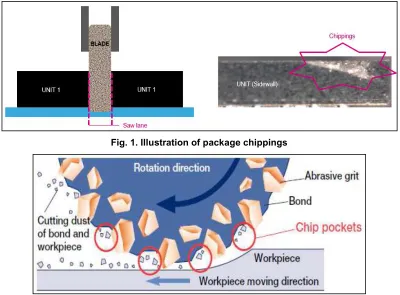
Failure such as package chippings is attributed to the abrasion process manifesting when the mechanical blade produces excessive damage in the plastic mold material typically localized near the saw lane (edges of the IC unit), shown in Fig. 1.
The wearing of mechanical blade affects the consistency of the cutting performance wherein as the actual application become longer, the cutting quality gradually decreases. This scenario is also similar to the occurrence of metal burrs in the said stations, wherein the un-removed metal
becomes physically connected between two isolated connections (leadframe leads or unit input/output (I/O)). The wearing of mechanical blade is correlated to the gradual diminishing of chip pockets shown in Fig. 2 which is accountable in the amount of material a blade can removed.
On normal production, since the occurrence of package chippings and metal burrs cannot be completely eliminated from abrasion cutting, it is allowed to a certain degree of manifestation but with considerations to multiple production controls and inspection to avoid potential escapee [1-2].
An alternative QFN device is realized to provide solution to the existing assembly limitations through, (1) modification of the encapsulation technique and (2) exposed copper die bar design. This initiative aims to eliminate the
mechanical blade application and related
process of cutting which is identified as a contributor to recurring assembly rejection. Moreover, it is expected that the design and method discussed in this paper provides reliable alternative of simplified method of operations and manufacturing.
Fig. 1. Illustration of package chippings
2. DESIGN SOLUTION AND IMPROVE-MENT
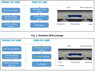
The standard QFN device is primarily composed of a silicon die bonded to a thermal pad through a conductive glue. The silicon die is connected to the leads by a conductive wire material then the overall unit is encapsulated by plastic molding material.
In producing a QFN device illustrated in Fig. 3, a series of assembly processes from Front-of-line (FOL) and End-of-line stations is required [3-8]. The FOL stations processed the bare unit (the silicon die is still exposed) while the EOL stations handles the encapsulated unit.
The objective of the novel idea is to replace the conventional singulation technique and eliminate the application of mechanical blade in separating the encapsulated unit. The novel idea can be realized through modification in the molding technique and addition of chemical etching process in the QFN assembly flow in Fig. 4.
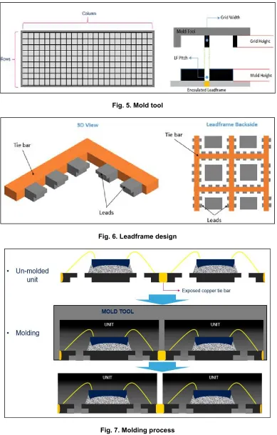
To achieve the design indicated in Fig. 4, the mold tool design is modified with “grid” design on
the internal mold chase. The grid or compartment dimension is equivalent to the package dimension requirement with the width of the
division corresponds to the pitching
measurement of the leadframe. Moreover, the height of the grid correlates to the mold height requirement of the unit, as shown in Fig. 5. The advantage of the compartment molding is to produce a “pre-cut” configuration in the encapsulated leadframe wherein the mold material is not physically connected to the neighboring unit.
The leadframe design highlighted in Fig. 6 is designed with full copper tie bar around the perimeter of the leadframe segments. It is required to be in this configuration to avoid the physical connection of the mold material to the neighbor unit during molding.
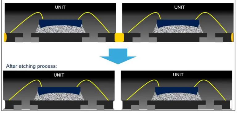
Fig. 7 shows the illustration of the leadframe with exposed tie-bar design when applied to the modified mold tool design. The un-molded unit that will undergo molding process can use the existing thermoset material or similar molding material in encapsulating the unit. Conventional machine can still be used to process the design
Fig. 3. Standard QFN package
Fig. 5. Mold tool
Fig. 6. Leadframe design
Fig. 8. Etching
thus there is no significant changes in the direct resources needed however in this design, the tolerance and alignment of carrier and mold grid design is crucial. It is recommended to implement tight control for tolerances.
Afterwards, the encapsulated unit will undergo etching process wherein the connecting copper tie bar will be removed. Afterwards, the unit can be separated individually from one another, as shown in Fig. 8. A metal plate designed with suction that is aligned to the location of each unit is advisable to remove the scattering of unit after copper tie bar is removed.
Removal of mechanical singulation process for the QFN assembly is possible with reference to this study. By removing the process, chronic assembly issues such as metal burrs and topside chippings can be removed as well. throughout the realization of this design, it is identified as potential reference to the future design of QFN and succeeding similar design of IC.
3. CONCLUSION AND RECOMMENDA-TIONS
An augmented QFN leadframe design is presented with a crescent configuration on the sidewall. The improved design is realized by the specialized process in package singulation which is the etching of the exposed copper tie-bar instead of the conventional package mechanical saw. The crescent structure of the
QFN package reinforces the mechanical
anchoring in the lead junction during board level application.
The combination of the improved leadframe design and process eliminates known assembly
rejection related to leadframe package
manufacturing. Discussions presented in some of the references [9-12] are helpful to mitigate defects related to assembly process.
DISCLAIMER
The products used for this research are commonly and predominantly use products in our area of research and country. There is absolutely no conflict of interest between the authors and producers of the products because we do not intend to use these products as an avenue for any litigation but for the advancement of knowledge. Also, the research was not funded by the producing company rather it was funded by personal efforts of the authors.
ACKNOWLEDGEMENT
The authors are thankful to STMicroelectronics Calamba colleagues and the Management Team for the usual great support.
COMPETING INTERESTS
Authors have declared that no competing interests exist.
REFERENCES
1. STMicroelectronics. Procurement and
2. STMicroelectronics. Assembly and EWS design rules for wire bond Interconnect dice. rev. 54.0; 2019.
3. Liu Y, Irving S, Luk T, Kinzer D. Trends of
power electronic packaging and modeling. 10th Electronics Packaging Technology Conference, Singapore; 2008.
4. Bacquian BC, Gomez FR. A study of wafer
backgrinding tape selection for SOI wafers. Journal of Engineering Research and Reports. 2019;6(2):1-6.
5. STMicroelectronics. Work instruction for
tap/DAF and glue diebond process. rev. 66.0; 2018.
6. Doering R, Nishi Y. Handbook of
semiconductor manufacturing technology.
2nd ed., CRC Press, USA; 2007.
7. May GS, Spanos CJ. Fundamentals of
semiconductor manufacturing and process control. 1st ed., Wiley-IEEE Press, USA; 2006.
8. STMicroelectronics. VMI criteria for
QFN/LGA packages. rev. 14.0; 2017.
9. Sumagpang A, Gomez FR. Line stressing
critical processes optimization of scalable package passive device for successful
production ramp-up. Journal of
Engineering Research and Reports. 2018; 3(1):1-13.
10. Rodriguez R, Gomez FR. Pick and place
process optimization for thin
semiconductor packages. Journal of
Engineering Research and Reports. 2019; 4(2):1-9.
11. Sumagpang A, Gomez FR. Introduction of
laser grooving technology for wafer
saw defects elimination. Journal of
Engineering Research and Reports. 2018; 3(4):1-9.
12. Gomez FR, Mangaoang T. Elimination of
ESD events and optimizing waterjet
deflash process for reduction of
leakage current failures on QFN-mr leadframe devices. Journal of Electrical Engineering, David Publishing Co. 2018; 6(4):238-243.
© 2019 Rodriguez et al.; This is an Open Access article distributed under the terms of the Creative Commons Attribution License (http://creativecommons.org/licenses/by/4.0), which permits unrestricted use, distribution, and reproduction in any medium, provided the original work is properly cited.
Peer-review history: