5
VIII
August 2017
742
©IJRASET (UGC Approved Journal): All Rights are Reserved
A Novel Optimized Multiplexer Design in
Quantum-Dot Cellular Automata
Soudip Sinha Roy Amity University, Noida
Abstract: Molecular quantum-dot cellular automata (QCA) is an emerging nanocomputing paradigm, which operates on electrostatic repulsion phenomena between two electrons to keep those apart at the maximum distance to a rest position for obtaining the highest finding probability. In the field of Quantum-dot Cellular Automata the digital logic gate approaches nearly about to nanometer in scale. In QCA quantum gates operate by the tunneling effect of electrons from one quantum dot to another dot through revealing its wave nature. The operating speed of the device gains the speed of light because the quantum tunneling occurs at the light speed. This paper compares two methodologies of quantum logic gate designing, those are universal T gate designing and conventional gate designing practice. One 22 cells 2x1 MUX is proposed which is designed by conventional method, that provides 20.35% optimization in area occupancy compared to the best reported designs. Furthermore, one 11 cells 2:1 MUX layout is proposed which achieves 33.33% area reduction compared to the best ever multiplexer designed in QCA technology.
Keywords: T gate; Electron tunneling gate; Multiplexer; quantum computing.
I. INTRODUCTION
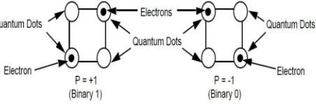
[image:2.612.189.415.413.488.2]Invention of Quantum Dot Cellular Automata is a revolutionize instance of the modern nanotechnology. Usually one quantum cell contains two electrons those are separated by mutual columbic repulsion at a maximum distance in quantum a cell, as fig. 1. As the following figure exhibits, one cell has maximum four quantum dot handling capacity along with two electrons. The electrons are switchable from one dot to another dot by means of tunneling.
Fig. 1: Quantum Cell architecture
This paper compares T universal gates and the conventional QCA universal gates adequately to briefly imply the effectiveness of T gate. Power utilization for the operation of logic gates are mathematically calculated and compared. Whereas, it is observed that the T gate is more useful and sophisticated for the implementation of the quantum logic gates.
II. CONVENTIONALQCALOGICGATES
Quantum Dot Cellular Automata technology involves two electrons at a time for tunneling to evaluate a logic state. Often the available papers from the QCA publication database, deal with the conventional logic gate implementation technique, where a bulk number of gates are found severally [5]–[7].
QCA device logic implementation technique is highly concentrated by five cells Majority Voter (MV) implementation technique. Majority output waveform is mathematically stated as, Z= AB+BC+CA.
Now A and B are the input bits and C is reserved as a control bit by which the polarization of the device is controlled dynamically. Once C is -1, that defines negative polarization state P (A, B). Then the MG (majority gate) expression becomes [4], Z=AB. Under this condition the gate turns to AND gate.
743
©IJRASET (UGC Approved Journal): All Rights are Reserved A. AND Gate Design
The AND gate contains five cells mostly. Hence, the polarization C is set to -1 which asserts binary logic state 0, fig. 2 (a). Due to the influence of the input signals the output comes out as an AND. Hence the majority gate expression becomes Z= AB. Which implies a AND gate [5]–[8].
Fig. 2: (a) AND gate designing using majority logic gate in conventional technique, (b) Simulation result
The simulation result of this gate, fig. 2 (b), always maintains the standard truth table of AND gate. From the above simulation result it is clearly visible that the output strength is only at a high logic level, where A=B= 1. This proves this gate has been configured as AND gate.
B. OR Gate Design
In the sense of OR gate the control C is to be set to 1 always, which provides positive polarization [9], [10]. Hence, the majority gate expression comes out as, Z=A+B after putting the input variables accordingly. Following fig. 3 (c), shows the OR gate layout followed by its simulated output waveform, fig. 3 (d).
Fig. 3: (c) OR gate layout, (d) Simulation result
From the above simulation result it is clearly visible that the output waveform remains high until the A=B=0. This results if any one input is high then the output goes high. Simulation result, fig. 3 (d) shows that this designed gate follows the standard truth table of OR gate.
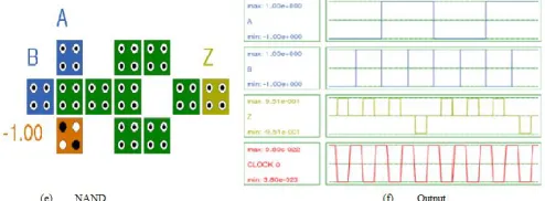
C. NAND Gate Design
NAND gate is an inverted form of the AND output as well it is known as the universal gate. In this circuitry the AND output is fetched through a NOT gate which complements the original output waveform [10]–[12] for generating the actual output of NAND gate. As an expression the output could be emphasized as, Z = . This total transition occurs within a single clock cycle i.e. 0th clock, fig. 4 (e).
[image:3.612.182.429.147.244.2] [image:3.612.188.424.377.480.2] [image:3.612.183.430.613.704.2]744
©IJRASET (UGC Approved Journal): All Rights are Reserved
[image:4.612.181.434.165.242.2]In the simulation result the output becomes high when two inputs A and B remains high, which shows the exceptional characteristic of digital logic family, i.e. NAND gate.Simulation result of the NAND gate expresses the physical characteristics of the NAND gate whereas the inputs are A, B and Z denotes the output, fig. 4 (e). The following waveform of the NAND gate exactly resembles with the standard NAND gate output, fig. 4 (f) [9], [13]. Table I, provides the truth table of the NAND gate which has received from the simulated waveform of NAND gate, fig. 4 (f).
TABLE I: NAND GATE TRUTH TABLE
A B Z
0 0 1
0 1 1
1 0 1
1 1 0
This truth table satisfies the perfection of the NAND gate design, whereas the output waveform, fig. 4 (f) is just a replica of this truth table, as table I.
D. NOR Gate Design
NOR gate also provides an inverted output waveform of the OR gate, whereas the OR output is subjected to a NOT gate to have the inverted output of the OR waveform. To design the NOR gate total number of used quantum cells is 12. These cells are well shaped in such a way that it is able to provide the inverted output waveform of OR gate when the input combination is introduced to this circuit, as fig. 5 (g). The output expression is given as Z= + .
Figure 5: (g) NOR gate layout, (h) Simulation result
The simulation result justifies that, the designed logic circuit is able to provide the NOR output depending upon the control C. In this case of operation the control is kept to 1 to get the OR output and thereafter the output is fetched as the input of the NOT gate for inverting the output, as fig. 5 (h).
This waveform in the simulation window, fig. 5 (h) shows that the output waveform always maintains the truth table, as table II. TABLE II: NOR GATE TRUTH TABLE
A B Z
0 0 1
0 1 0
1 0 0
1 1 0
III. LOGICGATEIMPLEMENTATIONUSINGT-GATEMETHODOLOGY
T-gate methodology of Quantum Dot Cellular Automata deals a sophisticated designing procedure for the universal logic gates by means of quantum tunneling. Here the T-gate is implemented by four quantum cells keeping three cells horizontally and one cell vertically along with them at the midpoint of the coplanar wire, fig. 6 (i). This gate comprises the universal logic designing scheme with a very less number of quantum cells. In the conventional gate designing technique the total number of used cells is 12, which is used to implement the NAND gate, as fig. 4 (e) [1]–[6].
[image:4.612.183.425.355.465.2]745
©IJRASET (UGC Approved Journal): All Rights are Reserved
propagation delay of the signal from one cell to another one gets reduced [14]. Apart from that the area utilization of the NAND gate using T universal methodology is efficient, table III. The area occupancy of the cells upon the cell bed tend to very less. In that case the device performance increases compared to the conventional technique.
A. T NAND Gate Designing
Universal T methodology provides a better perfection and efficiency towards the implementation of several kind of combination or sequential circuits. It is well known that any kind of logic gates can be implemented by two universal gates only i.e. NAND and NOR. For this reason these two gates are crucial to implement any kind of logic gates [15].
This T gate works as a NAND gate at a fixed control polarization C= 0.40 and works as NOR gate at C= -0.40. Hence to implement the NAND gate the fixed polarization C is kept to 0.40 polarization [1], which provides a particular orientation to the electrons to be settled after tunneling through the tunneling barrier. This T gate operates by the concept of partial polarization effect. The polarization 1 is always taken as an unite or primitive polarization. But 0.40 or -0.40 polarization is the partial polarization. Afterwards the output becomes as a NAND gate as fig. 6 (j) [10], [16].
Figure 6: (i) T NAND gate layout, (j) Simulation result
The simulation result shows the perfect waveform of the circuit shown in fig. 6 (e). The waveform in fig. 6 (j), is compatible enough to prove the NAND gate characteristic. The table was extracted out from the NAND simulation result, as fig. 6 (j). Now this waveform also provides the same values, as given in table III. Hence this is to be concluded that the NAND gate is successfully designed by T gate methodology [17]–[19].
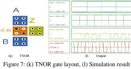
B. T NOR Gate Designing
For designing of the NOR gate the control polarization C is kept to -0.40, whereas it gives an opposite reflection of the polarization which is used to design the NAND gate [1], fig. 7 (k). Afterwards it is seen that the output waveform is obeying the standard output waveform of NOR gate. Hence this gate reveals the characteristics of NOR gate, as fig. 7 (l).
Figure 7: (k) TNOR gate layout, (l) Simulation result
Output waveform ensures about the successful implementation of NOR gate by T universal gate methodology, as fig. 7 (l).
Table Iii: Comparisons Of Area Utilization Factor
Sr. NO.
Designs Effective areas (nm2)
AUF
[image:5.612.187.408.263.358.2] [image:5.612.203.420.495.609.2]746
©IJRASET (UGC Approved Journal): All Rights are Reserved
This table shows the effective areas of corresponding designs accordingly with their area utilization factors (AUFs). AUF is a factor which shows the designing efficiency in terms of area utilization. The AUF is mathematically defined as,
AUF=
As much this factor becomes lesser, the designing quality become very higher. From table III, it is seen that the T-gate has the maximum efficiency rather than conventional universal gates in terms of AUF. This area calculation methodology is literally same with the calculation which is shown in section V for 2x1 MUX AUF calculation.
IV. XORGATEDESIGNINCONVENTIONALMETHOD
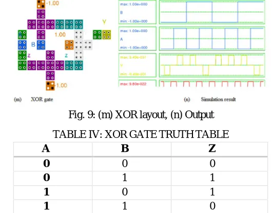
XOR stands for exclusive OR logic which layout shown in fig. 8 (m). This gate contains two AND and one OR gate associatively. In terms of XOR gate the main fundamental thing is this gate works as a buffer when anyone of the input is kept to zero (binary lower logic level) & when anyone of the inputs are in active high condition then this gate works as an inverter. This XOR gate is designed with 32 cells under four basic clocks. The given inputs of this gate are A & B, and Y is labeled as the output of this gate.
Fig. 9: (m) XOR layout, (n) Output
TABLE IV: XOR GATE TRUTH TABLE
A B Z
0 0 0
0 1 1
1 0 1
1 1 0
In the truth table, table IV the first two outputs show the buffer characteristic and the second two show the inverter characteristic.
[image:6.612.169.434.261.468.2]A. Layered T XOR Gate Design
Fig. 10: Layered XOR gate
V. PROPOSEDMULTIPLEXERDESIGN
Multiplexer is a combinational circuit which has several input lines but a single output line. This circuit is used to fetch the inputs in a proper manner according to the combination of select lines to the output line [1]–[7]. Having the multiple input handling capability this circuit is called multiplexer. If the total number of input lines are given by 2n then the number of select lines are always to be n [16].
[image:6.612.196.396.506.627.2]747
©IJRASET (UGC Approved Journal): All Rights are Reserved
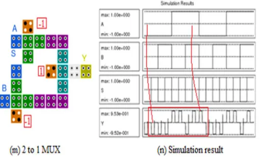
Here in this section one two input multiplexer layout is proposed which utilizes 22 cells to constitute the proper output waveform of 2x1 MUX. In this circuit the number of inputs are 21. So, as per the standard formula one select line is to be installed for this circuit i.e. S. A & B these two are the input data lines and correspondingly the Y denotes the output data line. The layout is designed in QCADesigner and simulated properly to express the output waveform of the multiplexer [16]–[19].
Figure 11: (m) 2x1 MUX layout, (n) Simulation result
Fig. 11 (m) shows the MUX layout in terms of 22 cells which is operated by four clocks. This gate contains two AND gate and one OR gate which simulates three inputs A, S & B intently to provide the output waveform as a 2x1 MUX, fig. 8 (n).
B. Effective Area Calculation
This layout has two dimensions one is length and another one is breadth. In the sense of QCA designing the standard spacing between two quantum cells is taken as 2nm. The spacing of the cells from the terminal point of the cell bed is 1nm. The cells are identical in area which is having 18nm length and 18nm breadth because of being a perfect square. Hence the area becomes 18×18 nm2 [1], [5], [12]-[21].
The calculated length of the proposed MUX is given by,
L=(1+18+2+18+2+18+2+18+2+18+2+18+2+18+2+18+1)= 160 nm. The breadth of the layout is given by,
W= (7×18+7×2) = 140 nm2.
Hence the area of the circuit is entirely given by, Area= L×W= 160 × 140 = 22400 nm2.
According to table V this design is most efficient design among all the previously proposed designs indexed in the table.
C. Optimized Area-Delay Efficient Multiplexer Design
[image:7.612.180.435.148.302.2]This multiplexer is developed only upon 11 cells which has the minimum latency and minimum area occupancy. This circuit is highly stable with lower radius effect.
[image:7.612.180.422.576.705.2]748
©IJRASET (UGC Approved Journal): All Rights are Reserved
List of inputs are: A, B, S. Among these inputs A is the most significant bit & S is the least significant bit, as fig. 12. The out of the multiplexer is mathematically expressed as Y= + . Therefore, the with the help of inputs signal bit combination the output bit sequence is given as {00011011}.
D. Driving (Fixed) Polarization Analysis for Proposed 11 Cells MUX
TABLE V: Fixed polarization analysis for proposed 11 cells MUX
Sr. No Fixed Polarizations Max Min
1 0.2 9.49 -9.49
2 0.3 9.49 -9.49
3 0.4 9.49 -9.49
4 0.5 9.48 -9.48
5 0.6 9.48 -9.48
6 0.7 9.48 -9.48
7 0.8 9.48 -9.48
8 0.9 9.48 -9.48
9 1 9.48 -9.48
[image:8.612.173.445.381.478.2]From the references, [3], [19] it is possible to configure a QCA circuit with partial polarizations. This partial polarization test is performed on the proposed 11 cells MUX. This rigorous investigation reveals that the output strengths are very stable if the circuit operates under partial polarization.
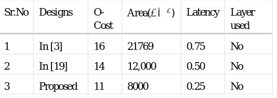
TABLE VI: COMPARISON WITH EARLIER DESIGNS
Sr.No Designs O-Cost
Area( ) Latency Layer used
1 In [3] 16 21769 0.75 No
2 In [19] 14 12,000 0.50 No
3 Proposed 11 8000 0.25 No
VI. RESULTSANDCONCLUSION
This paper contributes a brief comparison result between the T gate and conventional logic gate designing based upon QCA methodology. For the designing of all the mentioned circuits the most useful software QCADesigner is used. All the logic gates are successfully verified by the proper simulation results and with their respective standard truth tables of the basic gates as explained in section II & III. It is shown that the T gate is much efficient and truly effective compared to the conventional logic gate designing techniques in terms of AUF, effective area and the cell usages (O-Cost). One XOR gate is designed by the conventional technique which is expressed with its proper simulated output waveform. Comparative the layered T XOR gate is also presented which has 3 less cells compared to the layered XOR gate. The proposed 2x1 MUX design occupies 22400 nm2 area which is very lesser compared to previously published works on multiplexer designs, table VII.
Table VII: Comparison Table Of Effective Areas And O-Cost Sr.
No.
Proposed Designs O-Cost
Effective areas (nm2)
1 M. Askari et al. [17] 34 40764
2 A.Roohi et al. [18] 27 28124
749
©IJRASET (UGC Approved Journal): All Rights are Reserved
The proposed 11 cells 2:1 MUX is the revolutionized design for multiplexer layout which provides the best allover efficiency has ever found in QCA research, that has 33.33% reduction in area compared to latest design mentioned in table V and has 71.55% area reduction compared to the best conventional design in table VI.
REFERENCES
[1] Soudip Sinha Roy, "Simplification of master power expression and effective power detection of QCA device (Wave nature tunneling of electron in QCA device)," 2016 IEEE Students’ Technology Symposium (TechSym), Kharagpur, 2016, pp. 272-277. doi: 10.1109/TechSym.2016.7872695
[2] Soudip Sinha Roy, “An Intelligent Mathemetical QCA Power Analysis Technique in Wave Nature of Electrons”, proc. of IEEE 6th International Conf. on Cloud System and Big Data Engineering (Confluence), Noida, India, in press, pp. 689-693, 15th Jan. 2016.
[3] Chiradeep Mukherjee, Soudip Sinha Roy, Dr. Saradindu Panda, Dr. Bansibadan Majhi, “T- Gate: concept of partial polarization in quantum dot cellular automata”, proc. of IEEE 20th international conf. on VLSI Design and Test (VDAT), in press, India, 2016.
[4] Gino A. Dilabio, Edmonton (CA); Robert A. WolkoW, Edmonton (CA); Jason L. Pitters, Edmonton (CA); Paul G. Piva, Edmonton (CA), “Atomistic Quantum Dots”, Pub. No. US2015/0060771 A1, 5th May 2015.
[5] Mohammad Thaerifard, Mahmmod Fathy, “Improving logic function synthesis through wire crossing reduction in quantum-dot cellular automata layout”, IEEE trans. on Devices and Syatems, IET ciruits, vol. 9, no. 4, pp. 265-274, July 2015.
[6] Alan Olson, “Towards FPGA Hardware in the Loop for QCA Simulation”, published in Kate Gleason College of Engineering Rochester Institute of Technology Rochester, New York, May 2011.
[7] Géza Tóth, M. S, “Correlation and coherence in quantum-dot cellular automata”, published in Graduate School of the University of Notre Dame, Notre Dame, Indiana, July 2000.
[8] N. A. Shah, F. A. Khanday , Z. A. Bangi, “Quantum Cellular Automata Based Efficient BCD Adder Structure”, trans. on Communications in Information Science and Management Engineering (CISME), Vol. 2, No. 2, pp. 11-14, 2012.
[9] Saket Srivastava, Sudeep Sarkar, Sanjukta Bhanja, “Error-Power Tradeoffs in QCA Design”, proc. of IEEE 8th international conf. on Nanotechnology, pp. 530-533, Arlington, TX, 18-21 Aug. 2008.
[10] C. S. Lent, P. D. Tougaw, W. Porod, G. H. Bernstein, “Quantum cellular automata,” Nanotechnology, vol. 4, pp. 49–57, 1993.
[11] C. S. Lent, P. D. Tougaw, W. Porod, "Bistable saturation in coupled quantum-dot cells," Journal of Applied Physics, vol. 74, pp. 3558-3566, 1993.
[12] K. Walus, G. Schulhof, G. A. Jullien, R. Zhang, W. Wang, “Circuit Design Based on Majority Gates for Applications with Quantum-Dot Cellular Automata”, IEEE proc. ISSN 0-7803-8622-1, pp. 1354-1357, 2004.
[13] A.Sabbagh Mollahosseini, K.Navi C.Dadkhah,O.Kavehei, S.Timarchi, “Efficient reverse converter design for the new4-moduli sets{2n_1, 2n, 2n+1, 22n+1_1} and{2n_1, 2n+1,22n, 22n+1}based on new CRTs”, IEEE trans. on Circuitand Systems, vol. 57, no. 4, pp. 823–835, 2010.
[14] V. S. Dimitrov, G. A. Jullien, and K. Walus, “Quantum-dot cellular automata carry-look-ahead adder and barrel shifter,” proc. of IEEE Emerging Telecommunications Technologies Conf., 2002.
[15] K. Walus, T. Dysart, G. A. Jullien, and R. A. Budiman, “QCADesigner: A rapid design and simulation tool for quantum-dot cellular automata,” IEEE Trans. Nano., vol. 3, pp. 26–31, March 2004.
[16] V. C. Teja, S. Polisetti, S. Kasavajjala, "QCA based multiplexing of 16 arithmetic & logical subsystems-A paradigm for nano computing," in 3rd IEEE International Conference on Nano/Micro Engineered and Molecular Systems, NEMS 2008, pp. 758-763, 2008.
[17] M. Askari, M. Taghizadeh, K. Fardal, "Digital Design using Quantum-Dot Cellular Automata(A Nanotechnology Method," in proceedings of the International Conference on Computer and Communication Engineering, Kualalampur, Malayasia, 2008.
[18] A. Roohi, H. Khademolhosseini, S. Sayedsalehi, and K. Navi, "A Novel Architecture for Quantum-Dot Cellular Automata Multiplier," International Journal of Computer Science Issues, vol. 8, no. 6, Nov. 2011.
[19] Soudip Sinha Roy"pGate: An Introduction to A Novel Universal Gate and Power Drop Calculation of QCA circuits" International Journal Of Engineering And Computer Science (IJECS), https://www.ijecs.in, Volume 6 Issue 4, April 2017, 20967-20972, DOI: 10.18535/ijecs/v6i4.31
[20] Soudip Sinha Roy, Chiradeep Mukherjee, Dr. Saradindu Panda, Dr. Bansibadan Majhi, "Layered T Comparator using Quantum Cellular Automata", proc. of IEEE on Devices for Integrated Circuit (DevIC), At Kalyani, West Bengal, 2017, in press.