Advanced Low Power CMOS Design to Reduce
Power Consumption in CMOS Circuit for VLSI
Design
Pramoda N V
Department of Electronics and Communication Engineering, MCE Hassan Karnataka India
Abstract: Low power has emerged as a principal theme in today's electronic industry. Energy efficiency is one of the most critical features of modern electronic systems designed for high speed and portable applications. Reduction of power consumption makes a device more reliable and efficient. The minimum amount of power consumption was a major driving force behind the development of CMOS technologies. As a outcome, CMOS technology are best known for low power consumption devices. However, for minimizing the power consumption of system or device, simply knowing that CMOS devices may consume less power than equivalent devices from other technologies does not help much. It is important to know not only how to calculate power consumption, but also to calculate how various factors such as input voltage level, input rise time, source leakage current, Gate current, Switching power, short-circuit power, power-dissipating capacitor, and output loading affect the power requirement of a device. This paper presents an energy efficient and eco-friendly technique for overcoming power consumption in CMOS devices, focusing on calculation of power-dissipation in various components and, finally, the determination of various ways to reduce the total power consumption in a CMOS device. This technique has less power dissipation when compared to the conventional CMOS design style also the proposed technique is advantageous in many of the low power digital circuit design applications.
Keywords: Low power, power dispassion, energy efficient, source leakage current, gate current, switching power, gate capacitance, power reduction.
I. INTRODUCTION
Power consumption is one of the most important issues in VLSI circuit design for which CMOS is the prominent technology. Today’s focus on low power consumption is not only because of recent growing demands of mobile application but also for mobile battery powered electronic devices. Mobile industry itself provides path for innovation and potential for profitable jobs. Future progress in mobile electronics will depend on the development of inexpensive devices with complex functionality and long battery life. Even before mobile era power consumption was a major concern in all complex logic circuits. Even though many researchers proposed several energy efficient techniques they were not universally accepted. The aim of this paper is to show how devices circuits and architectures with in this design space may be optimized for minimum energy consumption. Traditional scaling of high performance FET’s uses a combination of supply voltage(Vdd) and threshold voltage(Vth) reduction to accommodate both performance and power requirements, but rapid rise of sub threshold and gate leakage has placed limits on this scaling strategy. It’s clear that the new strategies are necessary to address the power concerns in high performance devices.
II. THE HISTORY AND TREND OF POWER DESIPATION OF DIFFERENT COMPONENET OF CMOS
Technology (IJRASET)
Fig1: Chip complexity and trend in transistor integration over more than 2 decades.
Power dissipation has propelled due to transistor scaling, chip transistor count and due to clock frequencies. Sophisticated strategies to lower leakage and manage voltage and variability have strengthened in total power consumption. Since power reduction is mandatory in each application the trend for adjusting near constant clock frequencies also continues as shown below in frequency trend plot. Fig(2)
Fig2: Clock frequency Trend
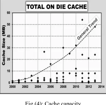
was done as shown in fig(4)
Fig (4): Cache capacity
In early electronics era power dissipation was very high since most of the devices contained only bipolar junction transistors this lead to the introduction of CMOS. The power dispassion comparison graph given below Fig(5)
Fig (5): Comparison of CMOS and BJT’s power dissipation.
III. MECHANISMS OF POWER DESSIPATIONS
Mechanisms of power dissipation are divided into two classes: dynamic and static power dissipation. Dynamic dissipation of power mainly occurs operational mode of the circuit eg. When the circuit is performing some other operation on the data. Static power dissipation becomes an issue when circuit is in inactive mode.
A. Dynamic Power Dissipation
It can be further divided into 3 major categories as: switched power dissipation, short circuit dissipation, and glitch power dissipation all these depends much on load capacitance, supply voltage and signal timing.
B. Static Power Dissipation
[image:4.612.226.404.106.283.2] [image:4.612.200.436.339.493.2]Technology (IJRASET)
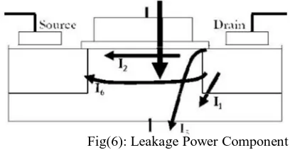
1) Leakage Power: Leakage power as a fraction of total power increases when the clockfrequency falls. Scaling down of FET’s requires lowering threshold voltage, which in turn increases leakage power.
Fig(6): Leakage Power Component
2) Junction Leakage: The PN junctions between diffusion, substrate and well are all junction diodes. These are reverse biased as substrate is connected to ground and well is connected to Vdd. But reverse bias leads to small amount of current.
Fig (7): Junction leakage due to reverse biasing.
IV. POWER REDUCTION TECHNIQUES FOR VARIOUS POWER DISSIPATING COMPONENTS
In the beginning of last decade, battery powered hand held devices evolved rapidly. This called for low power operation and lot of design methods on different hierarchy levels.
A. Voltage Scaling And Reduced Voltage Swing
Reducing the supply voltage is an attractive solution to reduce the power dissipation since both the switched and the short circuit power dissipation have a strong dependence on threshold voltage (Vth). Another way of sustaining the throughput is to do an architectural voltage scaling.
B. Clock Frequency Reduction
Reducing the clock frequency is not as beneficial as reducing supply voltage. However many processors in now a days have different power down modes where the clock signal is inactive to block the application that are unused at that moment. This process is known clock gating which can be used in most cases as conjunction with other low power techniques.
C. Switched Capacitance Reduction
Reducing the switched capacitance is similar power efficient as reducing the clock frequency of the circuit. Many advanced techniques have been proposed to reduce the switched capacitance. The selection of logic style can significantly affect the critical capacitances.
[image:5.612.201.405.115.221.2]We can reduce reverse IS leakage by varying the bias voltage both for high and low threshold voltage devices as given below
Fig (8): High and low Vth devices with respect to leakage current.
E. Reducing Gate Leakage Using Nitrogen And High K
Gate current depends more on dielectric material concentration (K) and temperature. We can limit gate current leakage by scaling appropriate material by selective use of ultra-thin surface modification layers and increased nitrogen concentration. Optimized dielectric stack reduces threshold shift by 200 to 300mV.Leakage current variation is in the diagram and graph is the variation of gate voltage wrt capacitance density.
Fig (9): gate vtg v/s capacitance density
F. Methods To Reduce Junction Leakages
Leakage modulation is primarily done at transistor doping level and band to band tunneling increases with doping levels.
V. VLSI CIRCUIT DESIGN TECHNIQUES FOR LOW POWER
A. Adiabatic Circuits
In adiabatic circuits power is reused instead of dissipating. It can be done by externally controlling length and shape of signal transitions. Diodes are not used in the design of adiabatic circuits because of thermodynamically irreversible in nature. MOSFET’s are not switched on when there is a potential difference between source and drain voltages and should not be turned off when there is a small amount of current flow in the circuit.
Fig (10): Adiabatic circuit- charge recovery logic
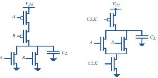
[image:6.612.190.434.118.216.2] [image:6.612.202.402.321.379.2] [image:6.612.214.407.540.635.2]Technology (IJRASET)
In case of static CMOS circuits power dissipation due to short circuit current is about 10% of total power consumption. But in dynamic CMOS we eliminated this problem since there is no direct DC path from supply voltage to ground.
Fig (11.a) Static Circuit (NOR gate) Fig (11.b) Dynamic Circuit (NOR gate)
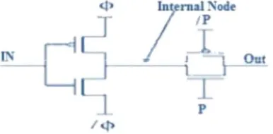
C. Reducing Glitches
Glitches usually occurs when two parallel driving common gate arrive at different times. This leads to incorrect output before resulting the actual one. The glitches can be reduced by using buffer circuit as shown below.
Fig (12): Buffer circuits
D. Logic Level Power Optimization
Power optimization is done by adjusting the parameters such as supply voltage and size of the gates path equalization by using buffer insertion, remapping transformation where high active node is removed and replaced by new mapping onto an AND or OR gate.
Fig (13): Remapping transformation In the fig ‘X’ indicates high active node
E. Standby Mode Leakage Supression
Leakage power originates from substrate currents and sub treshold leakages. Multiple treshold and variable treshold circuit techniques are often used to meet leakage power constraints.
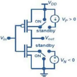
F. Variable Body Biasing
[image:7.612.179.435.113.240.2]Fig (14): Variable body biasing.
When circuit is in standby mode both the MOS’s are biased by third supply voltage to increase Vth as shown in the fig (14).
G. Sleep Transistors
Sleep transistors are high threshold voltage transistors connected in series with low Vth devices. When low Vth devices are ON sleep transistors will also be ON resulting normal operation. Since high Vth in series with low Vth leakage power is measured across high Vth devices thus resulting in lowering the static power dissipation.
Fig (15): Sleep transistors
H. Short Circuit Power Suppression
When pairs of PMOS and NMOS transistors are conducting simultaneously it leads to short circuit current then into short circuit power. The methods to reduce short circuit losses is to keep the input and output rise or fall time same. If Vdd<Vtn+|Vtp| then short circuit power can be eliminated. Similarly when load capacitance is very large output fall time is larger in comparison with input rise time then drain-source voltage of PMOS will be zero thus short circuit power also zero.
VI. A LOOK AT THE FUTURE
With what technologies we have today it is better to take some projection for next 10 years. If no steps have been taken in the circuit design technology then power dissipation will be bottleneck in chip design industries. As chip size reduces power dissipation should be in the managing limit so that chip will be reliable.
VII. CONCLUSION
Power consumption is associated with load capacitance, operation frequency, clock speed, supply voltage, threshold voltage, gate current and other factors like input and output rise time, output loading affect. Reduction of any of these is beneficial and provides economic, reliable circuits extended battery life of the electronic devices and helps to overcome problem associated with high temperature and need of heat sinks.
[image:8.612.245.373.113.241.2]Technology (IJRASET)
Electronics Module,” Proceedings of the 15th IEEE Semiconductor Thermal Measurement and Management Symposium
[3] S.Samanta“ Power Efficient VLSI Inverter Design using Adiabatic Logic and Estimation of Power dissipation using VLSIEDA Tool” Special issue of
International Journal of computer communication Technology.vol 2.isuue 2,3,4.pp300-303. 2010.