*[email protected]; phone 353 1 608-3802; fax 353 1 677-2442;http://www.tcd.ie; Department of Electronic & Electrical Engineering, University of Dublin, Trinity College, Dublin 2, Ireland; [email protected]; phone 353 1 606 7000; Intel Ireland Ltd., Collinstown Industrial Park, Lexlip, County Kildare, Ireland.
Study of structure and quality of different silicon oxides using FTIR
and Raman microscopy
C. Moore
a, T.S. Perova*
a, B. Kennedy**
b, K. Berwick
c, I.I. Shaganov
d, and R.A. Moore
aa
Dept.Electr.& Electr. Eng., Trinity College, Ireland;
bIntel Ltd., Ireland;
cDept. Electr. & Commun.
Eng., DIT, Kevin Street, Ireland;
dVavilov State Optical Inst., St.Petersburg, Russia.
ABSTRACT
In this work, SiO2 and fluorine and phosphorous doped SiO2 thin films are investigated using FTIR and Raman
techniques. FTIR spectroscopy was performed at normal and oblique incidence of the probe beam in transmission and reflection modes. The effect of polarisation and angle of incidence of the probe beam is examined for the case of reflection mode. Infrared spectra taken from doped oxides show that the structure changes with the passage of time. Alternate methods to calculate the thickness of the doped film are also discussed. Infrared spectra of electron beam evaporated oxides give valuable information on their structure and water content. The porosity is calculated for these samples. Finally, micro-Raman spectroscopy is used to measure the fluorine content in a device structure.
1. INTRODUCTION
Investigation of the structure and the defects present within thin films formed on silicon is crucially important in microelectronics. Fourier Transform Infrared (FTIR) spectroscopy provides a direct probe of molecular and submolecular structures via the excitation of vibrational states in the molecules over a specific mid -IR range (400-5000cm-1) [1-8]. Raman spectroscopy has been utilised recently to investigate stress and phase transformation in silicon structures [9-14]. The greatest advantages of both these techniques are its non-destructive character, the simplicity of the equipment set-up and the short time required for obtaining data, with essentially no sample preparation process required and no surface damage. The application of these powerful techniques allows information on the structure, stress, thickness, porosity, density, carrier concentration and several other important properties of thin films to be obtained. In this paper, a number of thin films are investigated; namely SiO2, fluorine doped SiO2 and phosphorus
doped SiO2. Fluorine and phosphorus doped oxides were investigated since these are important materials in the
microelectronics industry. In particular, fluorine doped SiO2 has a low dielectric constant which decreases parasitic
capacitance. These films were deposited on silicon and aluminium substrates by thermal oxidation and electron beam evaporation. We also analysed a composition of SiO2 doped with fluorine within a FIB box in a technologically
patterned wafer in order to determine the concentration of fluorine in some important areas along the devices s tructure of this FIB box.
2. EXPERIMENTAL
2.1 Sample Preparation
Fluorine doped SiO2 films were deposited using a parallel-plate electrode Plasma Enhanced Chemical Vapour
substrate was dipped in HF to remove any native oxide. Two fluorine doped oxide samples with concentrations of 3.18 at. % and 5.13 at. % and one phosphorus doped sample with a concentration of 4.6 at %% have been used in this study. Evaporated SiO2 films with different thicknesses were deposited using electron beam evaporation onto silicon
substrates. They we re prepared by the vacuum evaporation of vitreous quartz pieces in a bell jar evaporator from a heated tantalum crucible. A high vacuum (≤1.3 x 10⁻³ Pa) and a high deposition rate (≥1.5nm s-1) were used to ensure that there would be no excess oxygen in the deposited films.
2.2 FTIR measurements
FTIR was performed at normal and oblique incidence of the probe beam in transmission and reflection modes. Transmission mode FTIR is possible only if the substrate is IR transparent and therefore cannot be employed to examine patterned wafers. Most devices are, however, multilayered and normally opaque to IR light. Infrared reflection-absorption spectroscopy (IRRAS) avoids this problem by examining the reflected light from a sample’s surface [8, 15-17]. IRRAS has the advantage of enhancing the absorption at the surface of a sample thus aiding the investigation of very thin films, which normally have weak absorption. Both IRRAS and oblique transmission techniques [5-8] also allow observation of the Longitudinal Optical (LO) phonons which cannot be detected otherwise. Also, the reflection-absorption measurements at two different angles allows one to measure the thickness of the layer by using the Fabry -Perot method.
Digilab FTS60A and FTS6000 FTIR spectrometers were used to carry out IR measurements. An IR spectrum of the original Si wafer was taken as the reference. The spectrum taken for the oxidised samples contained information on both the SiO2 layer and the Si substrate. By subtracting the Si reference spectrum from the sample spectra,
information could be extracted regarding the SiO2 layer only.
Both FTIR spectrometers are equipped with Perkin-Elmer variable angle reflection-absorption attachments. All spectra measured with the IRRAS method were collected as single beam spectra. To improve the signal to noise ratio, 128 scans are recorded, co-added and then averaged. A single beam reflectance spectrum was taken from an aluminium mirror and then ratioed with the sample’s single beam spectrum in order t o obtain the reflectance spectrum.
2.3 Raman measurements
Raman spectra were registered in backscattering geometry using a Renishaw 1000 micro-Raman system equipped with a Leica microscope and an XYZ motorised positional stage. Using the 100x magnification objective in the microscope and an Ar+ ion laser with a 514nm excitation line allows Raman imaging of the surface with a spatial resolution of ~0.7µm. All spectra were recorded with a low laser power of ~20mW. The auto-focus line-mapping facility of the Raman system has been employed in this study. This allows the collection of spectra at each point along the chosen line with a 0.1µm step and with automatic focusing of the laser spot onto the mapped area. 101 Raman spectra were collected along the chosen line (~10µm in length) in a FIB box starting at the CoSi-SiO2+P interface. The acquisition
time of 100s was used for all line-mapping sessions. 300s was required in order to register the Raman spectrum of the CoSi layer. For each line, the line-mapping experiment was performed at least four times. The results obtained in these four mapping session are similar.
3. RESULTS AND DISCUSSION
3.1 Doped Oxides
Typically, a few vibrational bands belonging to Si-O vibrations such as stretching vibrations at ~1080cm-1, Si-O bending vibrations at ~800cm-1 and rocking vibrations at ~450cm-1 will be observed in the infrared spectra of silicon dioxide [1-8]. As was shown in the past, the intensity of these bands can be used for oxide thickness determination.
If SiO2 is doped with fluorine, an additional peak appears in the spectrum centred at 945cm -1
silicon dioxide doped with phosphorus, an additional vibrational band belonging to P-O appears at ~1300cm-1 (see Fig. 2) [18].
Measurements were repeated for the doped oxide samples six months after initial deposition. It was found that the intensity of the Si-O-Si bond vibration was significantly reduced when compared to the as -grown oxide. The 460cm-1 and 1080cm-1 bands are reduced by more than half their original intensity for a 5.13 at. % fluorine doped oxide, while the 800cm-1 mode remains unchanged. This mode can, therefore, be reliably used for film thickness evaluation, unlike the 460cm-1 and 1080cm-1 bands. Fig. 2 shows the IR spectrum of a phosphorus doped oxide over time. The structure of the phosphorus doped oxide has changed, but not as much as for the fluorine sample. The 810cm-1 band is unaltered, as in the case for the fluorine doped sample. It is presumed that this happened because the doped SiO2 was not annealed
enough after the deposition. Due to this, the fluorine and phosphorus diffuse through the bulk oxide to the surface where they create haze particles in the same manner as it was observed in Refs. [19,20].
3.2 Comparison of Thermal and Evaporated Oxides
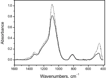
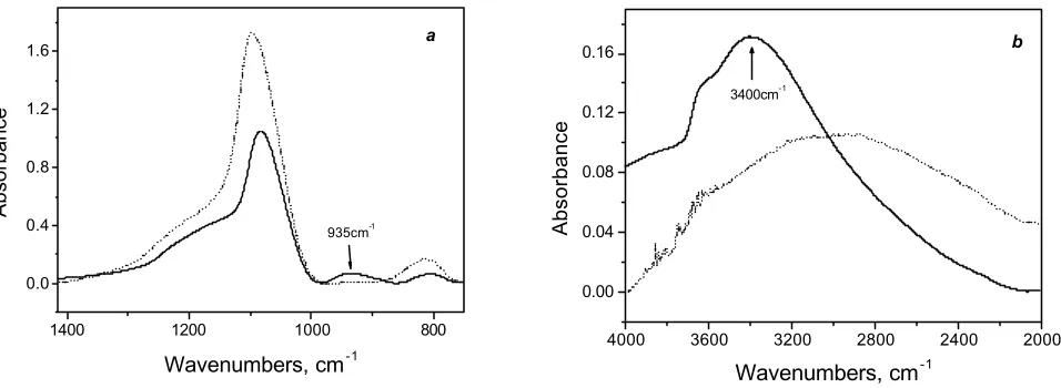
Fig. 3 shows the absorbance spectra for a 1µ m SiO2 film on silicon deposited by thermal oxidation and evaporation.
The spectrum of the evaporated oxide shows a pronounced difference in the intensity of the 1080cm-1 and 800cm-1 bands when compared to the thermally grown oxide (Fig. 3 a). This would indicate that the structure of the oxide is different for each case. In addition, the spectrum of the evaporated film shows the presence of a new band at 935c m-1. This band is attributed to the vibration of Si-OH groups, indicating that water has reacted with the SiO2 to form SiOH.
The presence of O-H and Si-OH groups will also affect the spectrum in the range 2500-4000 cm-1 (see Fig. 3 b). An absorbance band in this range was also analysed. The intensity of this wide band increases for the evaporated case with a maximum at around 3400cm-1 and is attributed to O-H stretching vibrations. The intensity of this band is directly proportional to the water content in the oxide as well as to the film porosity [21]. The evaporated oxide has a higher water content than the thermally grown oxide, indicating that the evaporated oxide is more porous. The OH groups present in the pores are negative ions and are not neutral like H2O. These ions will increase the refractive index and
give larger thickness readings when measured with ellipsometry.
The porosity of dioxides can be evaluated using FTIR data in the region of the O-H stretching vibration. The method suggested in Ref. [21] is applicable for the calculation of the open porosity of thin dielectric films from infrared spectra and has therefore been used. The open porosity, identical to the relative content of incorporated moisture, is given, in this case, by the ratio of the total intensities (or absorption coefficients) at the maximum of the bands of the absorbed
1400 1200 1000 800 600 400
0.0 0.8 1.6 2.4 3.2
Absorbance
Wavenumbers, cm-1
1600 1400 1200 1000 800 600 400
0.0 0.2 0.4 0.6 0.8 1.0
Absorbance
[image:3.612.61.274.242.401.2]Wavenumbers, cm- 1
Figure 1. FTIR spectra of fluorine doped (5.13 at. %) SiO2, measured after the deposition
[image:3.612.312.528.243.400.2](dotted line) and 6 month later (solid line).
Figure 2. FTIR spectra of phosphorous doped (4.6 at %) SiO2, measured after the deposition (dotted
and liquid water in the region 3000-3600 cm-1. Taking into account the local field acting in both cases on the water molecule in accordance with Ref. [22], the porosity V can be defined by the following equation:
∫
∫
− −=
ν
ν
ν
ν
ν
ν
d
q
K
n
d
q
K
n
V
w w w f f f)
(
)
(
)
(
)
(
2 2 (1)where the subscripts f and w respectively denote “film” and liquid “water”, K(ν) is Lambert-Bouger absorption coefficient in cm-1 and n is the refractive index. Assuming that the shape of the vibrational bands does not change upon absorption and using the mean values of the local field factors, qf and qw, in the Lorentz form (see [22] for details) we
can obtain:
%
100
)
2
(
)
2
(
2 2 max 2 2 max+
+
=
f w w w f fn
n
K
n
n
K
V
(2)The values of Kwmax and nwwere taken equal to 13028 cm-1 (at a frequency ~3350cm-1) and 1.27 respectively. The
absorption coefficient, Kfmax, for the SiO2 films was evaluated from the absorbance in the range ~3300cm -1
and thickness,d, using the following equation:
OH
A
d
v
K
(
)
=
2
.
303
(3)where AOH is the peak intensity of the O-H stretching vibration band in the measured absorbance spectrum. The
[image:4.612.67.545.423.598.2]refractive index, nf , is taken as 1.457 (typical value for an SiO2 film).
Figure 3. The comparison of FTIR spectra of electron beam evaporated SiO2 (solid line) and thermally grown dioxide (dotted line) in
the range of Si-O vibrations (a) and O-H vibrations (b).
Prior to calculating the porosity for the evaporated samples, the thickness had to be determined. This is not straightforward since the absorption intensity of the 1080cm-1 band for evaporated oxides is not the same as that for thermally grown oxides. Therefore, a new absorption coefficient needed to be ascertained for each absorption band in
1400 1200 1000 800
0.0 0.4 0.8 1.2 1.6 a 935cm-1 Absorbance
Wavenumbers, cm-1
4000 3600 3200 2800 2400 2000
0.00 0.04 0.08 0.12 0.16 b 3400cm-1 Absorbance
the spectrum shown in Fig. 3. This was achieved by analysing the interference fringes from EV1, the 1µm sample. Interference fringes provide a direct way to calculate the thickness rather than from the indirect absorption technique. The calculated thickness from interference fringes for sample EV1 was 1.04µm. This value and the absorbance (A) of each band was then substituted into Eqn. (4) to yield new values for
α
app which are summarised in Table 1.(
0)
0
434
.
0
log
x
x
I
I
A
=
=
α
app−
(4)where A is absorbance, I0 and I are the incident and transmitted intensities respectively, αapp is the apparent absorption
[image:5.612.179.415.286.348.2]coefficient,x0 is the native oxide (~15Å) and x is the oxide thickness (see Refs. [1, 2, 4] for details).
Table 1 Calculated absorption coefficients for 800, 935 and 1080cm-1 bands. The combined intensity of the 800cm-1 and 935cm-1
bands may be used with the appropriate
α
app.BAND αapp
800cm-1 0.142 x 104cm-1 935cm-1 0.157 x 104cm-1 935 & 800 cm-1 0.299 x 104cm-1 1080cm-1 2.349 x 104cm-1
[image:5.612.160.435.439.489.2]Using these coefficients the thickness, d, of each sample could be defined. The values are given in Table 2. Thickness measurements using ellipsometry are also shown.
Table 2 Sample thickness based on calculated values ofαapp, & ellipsometry.
SAMPLE THICKNESS,d(αapp) THICKNESS(ELLIPS.)
EV1 1.04µm 1.01µm
EV2 1913Å 1960 Å
EV3 112Å 208Å
The porosity can now be calculated from Eqns. (2) and (3) since both the thickness and absorbance intensity at 3400cm
-1
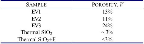
are available. From Table 3 it seems that the thinnest sample, EV3, is the most porous.
Table 3 Calculated porosity for samples EV1, EV2 and EV3.
SAMPLE POROSITY,V
EV1 13%
EV2 11%
EV3 24%
Thermal SiO2 ~ 3%
[image:5.612.179.417.592.666.2]This explains the figures given in Table 2 for film thickness. Ellipsometry and IR agree for samples EV1 and EV2, but ellipsometry gives almost double the thickness for EV3. This was due to the high water content in sample EV3, which is almost double that present in samples EV1 and EV2. OH groups present in the pores are negative ions and are not neutral like H2O. These ions will increase the refractive index and give larger thickness readings when measured with
ellipsometry. Care must be taken when analysing the results. This is because FTIR cannot differentiate between surface porosity and bulk porosity.
3.3 Thickness measurements with IRRAS
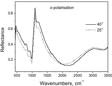
Fig. 4 shows IRRAS spectra for two angles of incidence with s-polarisation. The smooth structures between 1500cm-1 and 3500cm-1 are known as Fabry -Perot resonances [17] which are useful in the determination of the thickness of the oxide film. Note how the minima of the Fabry-Perot structures shifts to the high frequency side as the angle of incidence increases. The condition for the o bservation of the minima in the Fabry-Perot interference structure is [17]:
4
min
λ
m
nd
=
(5)whered is the film thickness, m is the number of the minimum (1 in the case of Fig. 4),
λ
is the wavelength (in µm),nis the refractive index of the film (1.462).
Since the IR beam is at an angle of incidence,
θ
, then the thickness dmay be calculated from Eqn. (6):θ
λ
nCos
m
d
4
=
(6)The term
Cos
θ
is used as a correction factor. Without it, d would be the path length of the IR beam and not the film thickness. [image:6.612.159.435.437.479.2]Using Eqn. (6) and the minima read from the spectra, the values of the film thickness given in Table 4 are calculated.
Table 4 Angle of incidence (
θ
) and calculated thicknesses.θ
MINIMUM THICKNESS25° 2063cm-1 0.92µm
40° 2166cm-1 1.03µm
The calculations are in good agreement with each other and ellipsometry, which measured the film thickness to be 1.00µm.
500 1000 1500 2000 2500 3000 3500 0.2
0.4 0.6 0.8
s-polarisation
Reflectance
[image:6.612.63.295.540.718.2]40o 25o
Figure 4. IRRAS spectra of 1µm SiO2 film
Interference fringes are observed if the spectrum is collected over a wide enough range and if the oxide film is thick. If the spacing between two fringe maxima or minima is known, then fringes can be used to define the first minimum of the Fabry -Perot resonance. The spectra in Fig. 5 are for SiO2 with 3% fluorine added. The oxide was deposited onto a
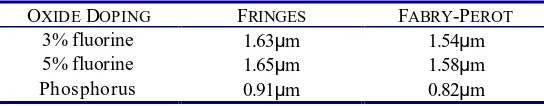
[image:7.612.162.434.238.291.2]silicon substrate. A comparison of film thicknesses as measured with fringes and Fabry -Perot resonance is shown in Table 5.
From Fig. 5 it is clear that the first minimum of the Fabry-Perot resonance is difficult to determine. In this case, the fringe method is used to calculate where the first minimum should be. Eqn. (5) can then be applied as usual. The thicknesses obtained as described above were used for porosity calculations and the results are shown in Table 3.
Table 5 Comparison of interference fringes and Fabry -Perot resonance for film thickness measurements. Results for 3% and 5% fluorine doped, and phosphorus doped oxides are given. The angle of incidence was 25° in all cases.
OXIDEDOPING FRINGES FABRY-PEROT
3% fluorine 1.63µm 1.54µm
5% fluorine 1.65µm 1.58µm
Phosphorus 0.91µm 0.82µm
3.4 Raman results
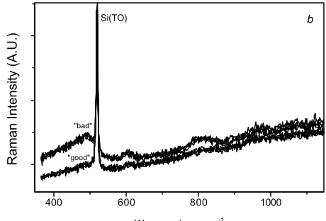
The Raman spectrum of crystalline silicon in a phonon region mainly consists of a narrow peak around 520cm-1 with a half-width of about 3.5cm-1 (see Fig. 6). The spectrum arises from scattering by long-wavelength transverse optical phonons [9-11]. This band is very intense, isolated and can be fitted by a single Lo rentzian curve shape. Removal of the background baseline followed by a line fit using a Lorentzian function allows three components of the Raman spectrum to be determined viz. intensity, half-width and position. These variations are related to the composition, defect density, and magnitude of stress respectively.
At higher acquisition times (100-300s), a number of additional bands (depending on the Si ingot growth process) become visible in the spectrum of crystalline Si. These bands for Czochralski grown silicon wafers appear at frequencies ~300cm-1 (2TA -transverse acoustical mode of the Si lattice) and at 605, 810 and 1060cm-1 [23]. The former few bands may appear due to the presence of different defects in the crystalline structure and, in particular, to the presence of oxygen and boron.
2000 4000 6000
0.2 0.4 0.6
0.8 SiO
2+513% F p-polaris. s-polaris.
Reflectance
[image:7.612.83.390.250.511.2]Wavenumbers, cm-1
Figure 5. IRRAS spectrum of 5.13 at. % fluorine doped SiO2 on silicon for s and
The Raman spectra of silicon dioxide and fluorine doped silicon dioxide looks quite different and consists of a number of vibrational bands which originate from the SiO2 network structure (bands at ~460, ~810, ~1065 and 1200cm
-1
) and from the breathing modes of fourfold and threefold ring defects (490 and 610 cm-1) [24, 25]. The position and the intensity of these bands will change with addition of fluorine. As was shown in Ref. [24], the increase in fluorine concentration leads to the increase in the intensities of bands observed at 490cm-1 and 960cm-1. At the same time, the addition of fluorine leads to the decrease in the intensities of bands observed at 610, 810 and 1060cm-1 (see Ref. [25]).
Bearing this in mind, we performed the comparison of the Raman spectra obtained from the same positions of the laser spot on the line along the FIB box in two devices (patterned wafers) with normal (“good” device) and abnormal (“bad” device) fluorine concentrations. (FIB box is the square cube cut into the silicon using a focused Gallium ion beam). The results of this comparison are presented in Fig. 6a-cfor spectra with the same order number (which corresponds to the same distance from the starting point 0) for both devices. As one can see from the spectra shown in Fig. 6 a, there is no noticeable difference between the Raman spectra for the good and bad devices in the range of distances 0 to 5.9µm (from the CoSi-SiO2+P interface). At the 5.9µm point, a noticeable change in Raman
spectrum of the bad device appears at 490cm-1 (see Fig. 6 b), which corresponds to the breathing mode of fourfold ring defects in the SiO2 network and this arises due to the increase of the fluorine concentration. The intensity of this band
still increases when we move to the ~7.0µm position and then decreases slightly after moving to the 8.0µm position. In the range 8.1 to 9.0µm, the Raman spectra for both devices look quite similar (not shown). However, in the range 9.1 to 10.0µm (Fig. 6 c) the difference between the Raman spectra for these two devices appears again, but this time the band at 490cm-1 appears in the spectrum of the good device only.
400 600 800 1000
a
"good" "bad"
Si (TO)
Raman Intensity (A.U.)
Wavenumbers, cm-1
400 600 800 1000
c
"good"
"bad"
Si(TO)
Raman Intensity (A.U.)
Wavenumbers, cm-1
400 600 800 1000
b
"good" "bad"
Si(TO)
Raman Intensity (A.U.)
[image:8.612.310.540.336.492.2]Wavenumbers, cm-1
Based on this observation, we can conclude that in the “bad” devic e (with respect to the “good” device) the excess of the fluorine concentration is observed along the distance 5.9 to 8.0µm from the CoSi-SiO2+P interface and a deficiency of fluorine concentration is found in the range 9.1 to 10µm.
It is difficult to determine the fluorine concentration in a FIB box quantitatively due to the presence of the much stronger Si phonon line closely beside the band at ~490cm-1, special care should be taken in order to eliminate the influence of this strong band. This can be done by the deposition of a thin Al layer (~0.1µm thick) between the Si substrate and SiO2+F layers. This Al layer will eliminate possible scattering from the Si substrate and thus the much
stronger Raman signal will be eliminated (or at least substantially suppressed). This will allow proper registration of the band at 490cm-1.
It should be noted that during this study our attempts to use for this analysis other fluorine bands in the high frequency region (600-1300 cm-1) were felt due to the overlapping of these fluorine bands with the bands belonging to the Si substrate. The presence of the vibrational bands belonging to the Si substrate in the Raman spectrum taken from inside of the FIB box is due to the diffraction effect at the FIB box edges. Using a long focus 100x objective in the Leica microscope instead of a short focus one (used in present study) can eliminate this effect.
4. CONCLUSIONS
The intensity of the absorption bands were used to determine the thickness of doped SiO2 films. The band at 945cm -1
provided sufficient information for this purpose. Care must be taken not to confuse the fluorine band at 945cm-1 and the band at 935cm-1 observed in the spectrum of the evaporated oxide. Careful examination of the spectrum of the evaporated oxide shows the 935cm-1 and 810cm-1 bands quite similar in intensity and shape, while the fluorine band at 945cm-1 tends to be somewhat smaller when compared to the 810cm-1 band. Investigations of doped oxides show that their structure changes over time. Although the intensity of the 1080cm-1 and 460cm-1 bands decreased with time, the 800cm-1 band did not appear to change. This band, therefore, could be used for film thickness evaluation provided an accurate value for αapp was calculated. The effect was mo re pronounced for the case of the phosphorus doped sample.
Also, the interferences fringes remained constant for each sample, enabling the accurate determination of the oxide thickness.
The porosity of SiO2 films was calculated. Care must be taken when analysing the results since FTIR cannot
differentiate between surface porosity and bulk porosity. This is a disadvantage of infrared spectroscopy insofar as it is not possible to discern whether porosity is constant throughout the bulk material or localis ed at the film surface. Interference fringes only appear in the spectrum if the oxide is thick enough. Transmission infrared measurements also benefit from a thicker oxide. For this reason, it was preferable to measure the thickness of the thin oxide samples by IRRAS. These thickness calculations were performed by using the Fabry -Perot resonance structures that appeared in the spectrum regardless of film thickness. The excess and deficiency of the fluorine concentration have been determined using Raman line-mapping experiments in a FIB box of devices with normal (3.18 at. % F in SiO2) and abnormal
fluorine concentrations. It has been found that at higher fluorine concentrations the intensity of the band at 490cm-1 is increases substantially.
ACKNOWLEGMENTS
CM wishes to thank Intel, Ireland for financial support of this work through the Postgraduate Studentship Programme.
REFERENCES
1. I.W. Boyd and J.I.B. Wilson, “A study of thin silicon dioxide films using infrared absorption techniques”,
J.Appl.Phys.53, pp. 4166-4172, 1982.
2. P.G. Pai, S.S. Chao, and Y. Takagi, “Infrared spectroscopic study of SiOx films produced by plasma enhanced
3. W.A. Pliskin, “Use of infrared spectroscopy for the characterisation of dielectric films on silicon”, in
Semiconductor silicon, ed. By H.R. Huff and R.R. Burgess, Electrochemical Society, Pennington, NJ, 1973, pp.
506-529.
4. G. Lukovsky, M.J. Mantini, J.K. Srivastava and E.A. Irene, “Low-temperature growth of silicon dioxide films: a study of chemical bonding by ellipsometry and infrared spectroscopy”, J.Vac.Sci.Technol. B5, pp. 530-537, 1987. 5. R. A. B. Devine, “Structural nature of the Si/SiO/sub2/ interface through infrared spectroscopy,” Appl. Phys. Lett.
68, pp. 3108-3110, 1996.
6. J.E. Olsen and F. Shimura, “Infrared spectroscopy of thin silicon dioxide on silicon”, Appl.Phys.Lett. 53, pp. 1934-1936, 1988.
7. C.T. Kirk, Phys. Rev. B38, pp. 1255-1273, 1988.
8. I.I. Shaganov, T.S. Perova, R.A. Moore and K. Berwick, Spectroscopic characterisation of SiO and SiO2 solid
films: Assignment and local field influence, J.Material Science: Materials in Electronics,12, pp. 351-355, 2001. 9. M.J. Pelletier, Analytical applications of Raman spectroscopy, 1999.
10. G.Turrell, J. Corset, Raman microscopy, Academic Press, 1996.
11. I. De Wolf, “Micro-Raman spectroscopy to study local mechanical stress in silicon integrated circuits,” Semicond.
Sci.Technol. 11, pp. 139-154, 1996.
12. K. Ajito, J.P.H. Sukamoto, L.A. Nagahara, K. Hashimoto, A. Fujishima, “Strain imaging analysis of Si using Raman microscopy,”J.Vac.Sci.Technol. A 13, pp. 1234-1238,1995.
13. S. Webster, D.N. Batchelder, D.A. Smith, “Submicron resolution measurement of stress in silicon by near-field Raman spectroscopy,” Appl.Phys.Lett.72, pp.1478-1480, 1998.
14. M Nolan, T.S. Perova, R.A. Moore, C.J. Moore, K. Berwick and H.S. Gamble, “Micro-Raman study of stress distribution generated in silicon during proximity rapid thermal diffusion”, Mater.Sci. & Engineering,B73, pp. 168-172, 1999.
15. O.P. Konovalova, O.Yu. Rysakova and I.I. Shaganov, “The determination of the optical constants thin films evaporated onto the metal in vacuum from IR reflection”, Sov.J.Opt.Technol.55, pp. 402-404, 1988.
16. K.B. Kent, A. William, A. Schmidt and E. Butler, In situ reflection absorption spectroscopic characterisation of plasma enhanced chemical vapor deposited SiO2 films, J. Appl.Phys., 64, pp.4704-4710, 1988.
17. P. Grosse, B. Harbecke, B. Heinz, R. Meyer, M. Offenberg, “Infrared spectroscopy of oxide layers on technical Si wafers”,Appl.Phys. A39, pp. 257-268, 1986.
18. J.E. Franke, T.M. Niemczyk, and D. Haaland, “Infrared spectroscopic techniques for quantitative characterization of dielectric thin films on silicon wafers”, Spectrochim. Acta,50A, pp. 1687-1723 (1994).
19. T.S. Perova, C. Beitia, M. Nolan, R.A. Moore, J. McGilp and H. Gamble, “Borosilicate glass as a spin-on dopant source: FTIR and spectroscopic ellipsometry investigations”, (submitted for publication).
20. L.D. Madsen, A.C. de Wilton and J.S. Mercier, “Examination of the stability of borophosphosilicate glass films”,
Chemtronics,5, pp. 35-42 (1991).
21. A.F. Perveev, G.A. Muranova, & V.M. Zolotarev, Sov. Solid State Phys.,14, pp. 2510, (1972).
22. I.I. Shaganov, “Manifestation of local field effects in the properties of optical materials and coatings”, Sov. J, Opt.
Technol.,59, pp. 1-11, 1992.
23. Y. Gogotsi, C. Baek and F. Kirsch, “Raman microspectroscopy study of processing-induced phase transformations and residual stress in silicon,”Semicond. Sci. Technol.14 pp.936-944, 1999.
24. S.W. Lim, Y. Shimogaki, Y. Nakano, K. Tada and H. Komiyama, “Changes in orientational polarization and structure of silicon dioxide film by fluorine addition,” J. Electrochem. Soc.146, pp. 4196-4202, 1999