High Pressure Band Structure, Density of States,
Structural Phase Transition and Metallization in CdS
J.
Jesse Pius
1, A. Lekshmi
2, C. Nirmala Louis
2,*1Rohini College of Engineering, Nagercoil, Kanyakumari District, India 2Research Center in Physics, Holy Cross College, India
Copyright©2017 by authors, all rights reserved. Authors agree that this article remains permanently open access under the terms of the Creative Commons Attribution License 4.0 International License
Abstract
The electronic band structure, density ofstates, metallization and structural phase transition of cubic zinc blende type cadmium sulphide (CdS) is investigated using the full potential linear muffin-tin orbital (FP-LMTO) method. The ground state properties and band gap values are compared with the experimental results. The equilibrium lattice constant, bulk modulus and its pressure derivative and the phase transition pressure at which the compounds undergo structural phase transition from ZnS to NaCl are predicted from the total energy calculations. The density of states at the Fermi level (N(EF)) gets enhanced
under pressure, which leads to metallization in CdS. The pressure corresponding to structural phase transition from ZnS structure (B3) to the NaCl structure (B1) is 0.0168 Mbar in CdS. The metallization pressure PM is 6.9133 Mbar.
Keywords
Band Structure, Metallization, StructuralTransition, CdS, High Pressure
1. Introduction
The theoretical study on electronic band structure, density of states, phase stability and structural changes of crystalline materials play a basic role in Theoretical and Computational Physics as well as Chemical and Material Engineering, because the better understanding of the various physical and chemical properties of solids mainly depend upon their structure. Currently there is lot of interest in the study of structural changes and phase stability of materials under pressure. The physical and chemical properties of materials undergo a variety of changes when they are subjected to pressure [1].
In recent years there has been an increased interest in the effect of high pressure on materials [2]. Geologists have probed the behavior of materials under pressure for learning the physico-chemistry of materials near the center of the earth. There is a continued advancement and interest in the
high pressure studies due to the development of different designs of diamond anvil cell (DAC). With a modern DAC, it is possible to reach pressures of 2 Mbar (200 GPa) routinely and pressures of 5 Mbar (500 GPa) or higher is achievable [3]. At such pressures, materials are reduced to fractions of their original volumes. With this reduction in inter atomic distances; significant changes in bonding and structure as well as other properties take place. The increase of pressure means the significant decrease in volume, which results in the change of electronic states and crystal structure. It is an interesting phenomenon that pressure can change the electrical properties of matter. Generally it narrows the energy bandgaps of matter and hence the matter could transform from semiconductor to metal [1-8].
Recently, pressure induced phase transition of CdS was investigated using Raman spectroscopy and in situ electrical resistivity measurement on DAC by Wang et al [4]. In this study pressure induced phase transition of CdS was investigated by Raman spectroscopy and electrical resistivity measurement on DAC. Both of the experiments suggested the occurrence of the CdS phase transition from WZ to intermediate to RS phase. Besides, electrical resistivity measurements indicated that CdS undergoes semiconductor – metal phase transition under high pressure [4]. As a group II–VI semiconductor, cadmium sulfide has gained wide recognition because of its outstanding optical-electronic properties and polymorphic structural transformations. It has a direct band gap of 2.4 eV that lends itself to many applications in light detectors, forming quantum dots, and passivating the surfaces of other materials. Owing to the thermal stability and the colour in yellow, it can form pigments in colors ranging from deep red to yellow with the addition of CdTe [5].
semiconductors were given by Vladimir V. Shchennikov etal [6]. The indirect energy gaps of NaCl-structured CdS and CdSe are measured using absorption spectroscopy to approximately 55 and 42 GPa by Cervantes etal [7]. There is no high pressure studies related to metallization in CdS.This motivated us to take up the present investigation on CdS.
The electronic configuration of Cd and S are [Kr] 4d10 5s2
(Z = 48) and [Ne] 3s2 3p4 (Z = 16) respectively. The valence
electronic configurations 4d10 5s2 for Cd and 3s2 3p4 for S are
chosen in our calculation. We have obtained the band structures and density of states of CdS corresponding to various pressures using the full potential linear muffin-tin orbital (FP-LMTO) method [1, 8]. The calculated total energies were fitted to the Murnaghan’s equation of state(EOS) [1], todetermine the phase transition pressure and other ground state properties. Generally sulphide compounds (ZnS and CdS) crystallize in zinc blende structure (ZnS) [9, 10]. Group II-VI compounds undergo structural phase transition from zinc blende to NaCl structure prior to metallization. The phenomena of metallization at high pressure (NaCl) structure of CdS are analyzed. We give the details of the calculational procedure and electronic band structure corresponding to various pressures in Section 2. In Section 3, the ground-state properties, structural phase transition and metallization are discussed. Concluding remarks are given in Section 4.
2. Band Structure and Density of States
2.1. Calculational Procedure
Group II-VI semiconductor CdS crystallizes in zinc blende structure under ambient conditions and undergo structural phase transition from ZnS to NaCl structure. The electronic band structure calculations were performed for CdS corresponding to different reduced volumes both in ZnS and NaCl structures, by the first-principle linear muffin-tin orbital (FP-LMTO) method. We have used FP-LMTO method with in generalized gradient approximation (GGA) [1]. We have used the exchange-correlation potential of Ceperley and Alder as parametrized by Perdew and Zunger [1].We give here only the calculational details. The electronic configuration of Cd and S are [Kr] 4d10 5s2 (Z = 48)
and [Ne] 3s2 3p4(Z = 16) respectively. The valence electronic
configurations chosen in our calculation are 4d10 5s2 for Cd
and 3s2 3p4 for S .There are 18 valence electrons contributing
to the valence bands [1]. The final energy convergence is within 10–5 Ry. The calculated total energies were fitted to
Murnaghan’s equation of state (EOS) [2], to determine the bulk modulus and pressure derivative of bulk modulus Bo’. Theoretical studies of cohesive, structural and vibrational properties of solids under pressure are performed by means of FP-LMTO calculations [8-10]. We have obtained,
(i) normal pressure band structure and density of states of
CdS (with ZnS structure),
(ii) high pressure band structure and density of states of
CdS (with NaCl structure),
Also, we have analyzed the structural phase transition from ZnS→ NaCl structure and metallization. The radii of the Wigner-Seitz sphere are chosen according to the criterion for charge transfer from cation to the anion [11]. The entire Brillouin zone is partitioned into 4096 cubical volume elements and E (k) are computed for the k-points located at the center of each volume element. But because of the symmetry considerations this involves only 145 k points for both ZnS and NaCl structures, which are uniformly distributed in the 1/48-th of the first Brillouin zone [12]. In the calculation of total energy with NaCl structure, two empty spheres (ES) are positioned along the body diagonal (0.25 0.25 0.25) and (0.75 0.75 0.75) for closer packing and with the ZnS structure two empty spheres are introduced at positions (0.5 0.5 0.5) and (0.75 0.75 0.75) in such a way that they do not break the crystal symmetry. The calculated total energies are fitted to Murnaghan’s equation of state (EOS) [13], to determine the pressure derivative of bulk modulus Bo1, phase-transition pressure and other ground-state
properties [14,15]. The bulk modulus is a property of the material which defines its resistance to volume change when compressed. The cause for phase transition and the relation between phase transition pressure and atomic radii are deduced from band structure investigation [16, 17].
2.2. Band Structure and Density of States of CdS under Pressure
The band structures and density of states for CdS is computed for various reduced volumes ranging from V/Vo=1.0 to 0.3 in steps of
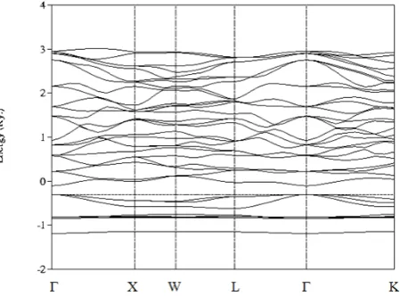
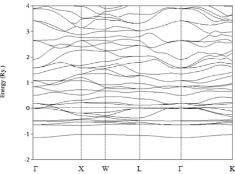
0.05 (Figs.1 to 4). But here we have presented the density of states and band structures along the symmetry directions Γ-X-W-L-Γ-K corresponding to volume compressions V/Vo=1.0 and V/Vo=0.3852 for CdS only (Figs.1and 2).
[image:2.595.320.545.533.699.2]Figure 2. Metallization pressure band structure of CdS (NaCl structure)
Figure 3. Normal pressure density of states of CdS (ZnS structure)
Figure 4. Metallization pressure Density of states of CdS (NaCl structure) In the bottom of the valence band, a single band is positioned due to 3s2 electrons of S (Figs.1 and 2). Below the
Fermi level, the three bands appearing due to the 5s2
electrons of Cd and 3p4 electrons of S (Fig.1). The
degenerate five bands are due to 4d10 electrons of Cd. The 5p,
5d states of Cd and 3d, 4s states of S produces the empty conduction bands above the Fermi level (Fig.1). The direct band gap at normal pressure is found to be 2.42 eV for CdS
(at Γ point). The increase in the width of the valence band and conduction band due to high pressure, leads to the narrowing of the band gap and finally metallization in CdS at V/Vo=0.3852 (PM = 6.9133 Mbar) (Fig.2 and Table.1).
Metallization occurs via direct closing of band gap in between Γ and X points (Fig.2). There is appreciable value for density of states at Fermi energy N (EF) at the
metallization pressure. We have given the DOS histograms of CdS corresponding to normal pressure (Fig.3) and metallization pressure (Fig.4). At normal pressure (Fig. 3) the short spike near the origin is due to the levels arising from 3s2 electrons of S. The long spike near the Fermi energy
is due to3p4 electrons of S. The 5p and 5d states of Cd and S
produce the short peaks above the Fermi energy EF. The
width of the valence band and the empty conduction band get widened, as the pressure increases. These changes lead to the closing of the band gap under pressure (Fig.4).
Table 1. Metallization and phase transition pressures in CdS
Cadmium Compound
Metallization Phase transition P M
Mbar (V/Vo) M Mbar P T (V/Vo) T
CdS 6.9133 0.3852 0.0168 0.975 When pressure increases ( reduced volume decreases)the value of the DOS at Fermi energy, EF (N(EF)) increases
[2].The normal pressure DOS trend is changed under high pressure. The increase of pressure leads to the broadening of bands and decrease of density of states value in most of the energy regions. It also increases the width of the valence band and empty conduction bands [1, 2]. When pressure increases, the value of EF increases whereas no density of
states is available at the Fermi level up to metallization pressure. Further increase in pressure leads to enhanced density of states at the Fermi level which induces superconductivity [4].
3. Results and Discussion
3.1. Ground State Properties
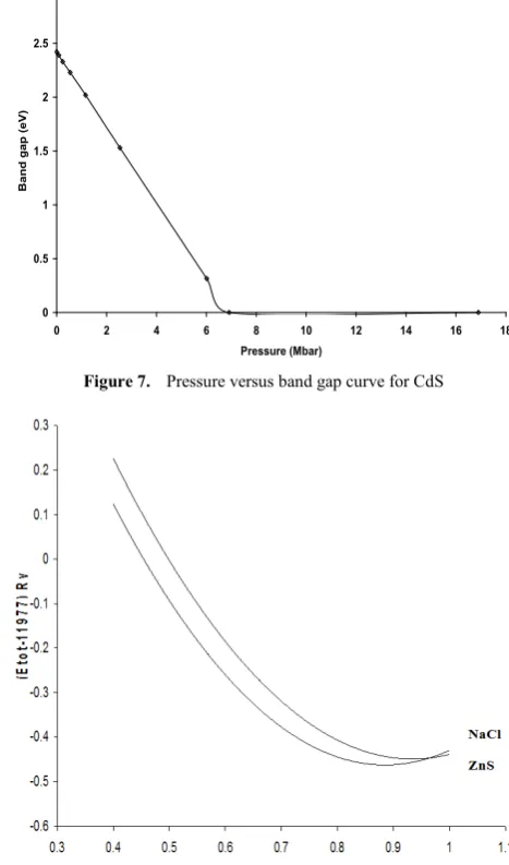
[image:3.595.60.298.467.637.2]The calculated reduced volumes, lattice constant and band gap values of CdS for different pressure are given in Figs 5,6 and 7 respectively. From the total energy as a function of reduced volume curve (Fig.8), it is found that, in CdS, up to V/Vo= 0.975 (PT = 0.0168 Mbar), ZnS structure has the lowest energy and on further reduction of volume NaCl structure becomes more stable in energy than the ZnS structure [18]. In Table 2, the equilibrium lattice constant (ao), band gap (Eg), bulk modulus (Bo) and its pressure
derivative (Bo1) values are compared with experimental [6,9]
and previous theoretical works [16,18]. From Table 2, it is observed that one gets larger lattice constant corresponding to smaller bulk modulus [1]. Our estimated bulk modulus of CdS is less than that of ZnS, as a result compressibility is higher for CdS than ZnS. Thus, it is noted that the compressibility decreases as the size of the cation decreases. This is the general trend in alkali halides [19], which is confirmed now for CdS.
P=1.5Bo[(Vo/V) 7/3 – (Vo/V) 5/3][1 +
+ 0.75 (Bo1- 4) {(Vo/V) 2/3-1}] (1)
0 0.2 0.4 0.6 0.8 1 1.2
0 2 4 6 8 10 12 14 16 18
Pressure (Mbar)
R
educ
ed v
ol
um
e
Figure 5. Pressure versus reduced volume curve for CdS
6 7 8 9 10 11 12
0 2 4 6 8 10 12 14 16 18
Pressure (Mbar)
Lat
tice
c
on
st
an
t (
au
[image:4.595.311.545.86.483.2])
Figure 6. Pressure versus lattice constant curve for CdS
0 0.5 1 1.5 2 2.5 3
0 2 4 6 8 10 12 14 16 18
Pressure (Mbar)
B
and ga
p (
eV
)
Figure 7. Pressure versus band gap curve for CdS
Figure 8. The total energy versus reduced volume curve for CdS
Table 2. Equilibrium lattice constant (ao), bulk modulus (Bo)and its pressure derivative (Bo1) of CdS in ZnS structure
Ground State Properties
CdS
Present
work Experimental work [6,9] theoretical works Previous [16,18] ao a.u. 11.002 11.0 10.81
Bo Mbar 0.72 0.73 0.69
Bo1 5.2 5.3 5.6
[image:4.595.304.548.275.498.2] [image:4.595.64.287.308.614.2]3.2. Structural Phase Transition
At ambient pressure CdS is in the ZnS structure. The phase stability of the B3 (ZnS) and B1 (NaCl) structures of CdS is analyzed using the enthalpy calculation [20,21]. The enthalpy H (P) is defined by
H (P) =Etot (P) + PV (P) (2) and the transition pressure corresponding to the phase transitionfromB3 to B1 is obtained from the relation
[image:5.595.60.295.193.374.2]HB3 (P) = HB1 (P) (3)
Figure 9. The pressure versus enthalpy curve for CdS
where HB3 and HB1 are the enthalpies of the B3 and B1 phases respectively. The pressure versus enthalpy curve for CdS is given in Fig.9.
From the enthalpy calculation, the phase transition pressure (PT=0.0168 Mbar) and the corresponding reduced
volume ((V/Vo)T = 0.975) are estimated for CdS (Table.1).
Our calculated phase transition pressure of CdS supports the experimental value of 0.02 Mbar [6]). The mechanism for the phase transition is a geometric effect involving a change in the coordination number from 4 in the ZnS phase to 6 in the NaCl phase [22, 23].
3.3. Metallization
At normal pressure, CdS is a direct band gap semiconductor [24,25]. The band gap decreases with the increase of the pressure and at a particular pressure, there is a closing of the band gap. The band structure corresponding to metallization of CdS is shown in Fig. 3. In CdS, the metallization occurs through direct closing of the band gap inbetween Γ and X points (Fig.2). In CdS, the direct closure of the band gap inbetween Γ and X point takes place at the reduced volume V/Vo=0.3852 (NaCl structure), the corresponding metallization pressure is 6.9133Mbar (Fig.2). For CdS, no experimental metallization value available for comparison. But our calculation is in agreement with the simple linear extrapolation data of Cervantes etal [7]. They estimated the metallization pressure of NaCl-structured CdS was above 250 GPa or 2.5 Mbar. Because phase transition occurs below this pressure and NaCl-structured phase will
undergo metallization [7]. Similar to group III-V compounds [22], prior to metallization, group II-VI compounds undergo structural transition from ZnS to NaCl structure [1, 4]. The values for density of states at Fermi energy N (EF) are very
small, at the metallization pressures, which indicate that metallization has just set in CdS (Fig. 4). Thereafter N (EF)
increases slowly with pressure and becomes fairly large at a particular value of V/Vo [20]. The values of EF and N (EF)
corresponding to different V/Vo are used in studying the pressure variation of superconducting transition temperature [26-29].
4. Conclusions
In summary, we have investigated the pressure dependent band structure, density of states, structural phase transition and metallization of cubic zinc blende type CdS using FP-LMTO method. Cadmium sulphide becomes metal under high pressure, but before that they undergo structural phase transition from ZnS to NaCl structure. The ground state properties and band gap values are compared with the experimental and previous theoretical results. When the pressure is increased there is enhanced overlapping between the wave functions of the neighbouring atoms. As a result the widths of the valence and empty conduction bands increase. The broadening of both the valence and conduction bands with pressure leads to the band gap closure and the formation of metallic states [26]. These changes lead to the narrowing and closing of band gaps in CdS (metallization). Our calculated phase transition pressure of CdS is (0.0168 Mbar) agreement with the experimental value of 0.02 Mbar. The mechanism for the phase transition is a geometric effect involving a change in the coordination number from 4 in the ZnS phase to 6 in the NaCl phase [27]. In CdS, the direct closure of the band gap in-between Γ and X point takes place at the reduced volume V/Vo=0.3852 (NaCl structure), the corresponding metallization pressure is 6.9133Mbar. For CdS, no experimental metallization value available for comparison. It is also confirmed that the metallization and structural phase transition do not occur simultaneously in CdS.
REFERENCES
[1] J. Jesse Pius and C. Nirmala Louis, Chemical and Materials Engineering 4(3): 46-56, (2016).
[2] V. Benaline Sheeba and C. Nirmala Louis, International Journal of Scientific Research and Innovations, 1, 1-5 (2016). [3] M. I. Eremets, K. Shimizu, and K. Amaya, Science 281, 1333
(1998).
[5] J.J. Tan, Y. Li and G.F. Ji, Acta Physica Polonica A, 120 (3), 501 (2011)
[6] Vladimir V. Shchennikov, Sergey V. Ovsyannikov, Physica status solidi (b), 244 (1), 437(2007).
[7] P. Cervantes, Q. Williams, M. Cote, O. Zakharovand M.L. Cohen, Phys. Rev. B, 54 (24), 17585 (1996).
[8] Mujica et al.: High-pressure phases of group-IV, III–V, and II–VI compounds Rev. Mod. Phys., Vol. 75, No. 3 (2003) [9] Edwards, A. L., and H. G. Drickamer, Phys. Rev. 122, 1149
(1961).
[10]O. K. Andersen, O. Jepsen and M. Sob, “Elctronic band structure and its applications”, edited by M. Yussouff (Springer, Heidelberg,1987)
[11]Mariano, A. N., and E. P. Warekois, Science 142, 672 (1963). [12]Rooymans, C. J. M., Phys. Lett. 4, 186(1963).
[13]Suzuki, T., T. Yagi, S. Akimoto, T. Kawamura, S. Toyoda, and S. Endo, J. Appl. Phys. 54, 748 (1983).
[14]Nelmes, R. J., and M. I. McMahon, Semicond. Semimetals, 54, 145(1998).
[15]Co te, M., O. Zakharov, A. Rubio, and M. L. Cohen, Phys. Rev. B 55, 13 025(1997).
[16]Dreysse, H., Ed., Electronic Structure and Physical Properties of Solids: The Uses of the FP-LMTO Method (Springer, Berlin) (2000).
[17] Holzapfel, W. B., and N. S. Isaacs, Eds, High-Pressure Techniques in Chemistry and Physics (Oxford University Press,) (1997).
[18]O. M. Madelung, Semiconductors: Data Handbook, 3rd ed. Springer, Berlin, (2004).
[19]C. Nirmala Louis and K. Iyakutti, Phys. Stat. Sol (b) 236, 614 (2003); Phys. Stat. Sol (b) 233, 339 (2002).
[20]S.Q. Wang and H.Q. Ye, Phys. Rev. B 66, 235111 (2002). [21]C. Nirmala Louis, A. AmalRaj and K. Iyakutti, Journal of
theoretical and computational Chemistry, vol.11, pg. 19-33 (2012).
[22]V. Benaline Sheeba and C. Nirmala Louis, Chemical and Materials Engineering 1(4): 132-140, 2013.
[23]A. Vladimir and R. Serget, Physica status solidi (b), Vol.244, 243-248 (2007).
[24]S.Q Wang and H.Q Ye, Journal of physics: condensed matter, Vol.14, 9579-9587 (2002).
[25] D. Fritsch, H. Schmidt and M. Grundmann Phys. Rev. B, 67, 235205 (2003).
[26] S.S. Saxena and P. Monthoux, Nature 427, 799 (2004). [27] N. E. Christensen and I. Gorczyca, Phys. Rev. B 47, 4307
(1993).
[28]I. Vurgaftman, J.R. Meyer and L.R. Ram Mohan, J. Appl. phys. 89, 5815(2001).