Journal of Chemical and Pharmaceutical Research, 2015, 7(12):84-90
Research Article
CODEN(USA) : JCPRC5
ISSN : 0975-7384
Experiment and analysis on stress of flip chip bonding process
Jiapeng Wang, Lezhi Ye* and Desheng Li
College of Mechanical Engineering and Applied Electronic Technology, Beijing University of Technology, Beijing, China
_____________________________________________________________________________________________
ABSTRACT
Flip chip bonding is an advanced microelectronic packaging technology, which has been developed rapidly in recent years. This paper mainly studies the stress of flip chip bonding process, which provides theoretical basis for the research and development of high density flip bonding equipment. The control of bonding force is a key technology of flip chip bonding process, which can directly affect the deformation of bumps. And the quality of bumps will affect the reliability of reflow soldering, filling glue in the bottom surface and other follow-up processes. In addition, the impact and volatility of bonding force will also result in fragmentation of brittle chip, so that the chip will be invalidation and scrapping. Therefore, based on the theory of stress intensity and aimed at the flip chip bonding, we establish the basic model of chip bonding in this paper. We have studied the relationship between bonding force and deformation of bumps and the relationship between bonding force and fragmentation of the chip by the simulation. And the finite element model is verified and modified based on the experiment result. Finally, we obtain an assessment method of the reliability of flip chip bonding, and this method can be used for the research and development of bonding equipment.
Key words: flip chip, reflow soldering, bonding force, bump deformation, chip fragmentation
_____________________________________________________________________________________________
INTRODUCTION
The electrical interconnection technology in chip level is one of the core technology of the packaging[1]. The interconnection technology mainly includes the wire bonding, flip chip bonding[2]and wafer bonding. At present, the packaging I/O ports are becoming more and more, and the performance requirement of internal connection is increasingly highly too, especially in the mobile phone and handheld consumer electronic products. Flip chip can be used to reduce the product size and improve product performance, so the application of which is becoming more and more widely. Currently, the mass production and most mainstream flip chip bonding process is the reflow soldering technology at home and abroad. The manufacture process of reflow soldering flip chip is that: firstly, the chip with Sn bumps is made upside down and dipped soldering paste; secondly, the chip is pressed onto the pads of substrate or lead frame, and the bumps and pads are connected through reflow oven; finally, the reliability of the connection is enhanced by filling glue in the bottom surface. The process is shown in Figure 1.
Fig1Process of flip chip packaging
Film
Flip chip
Dip flux Align Substrate Bond
Reflow Preheat
During the process of the flip chip manufacture and packaging, 40% failure is related to the bump damage and the chip breaking. In the case that the deformation of bumps is too large and the connection of bumps and the chip or pads is not good, it will lead to the bonding failure. If the chip is broken because of the fluctuation of bonding force or overlarge bonding force, it will bring fatal damage to the chip. So the bonding is a key technology to decide the quality of flip chip.
In recent years, the flip chip packaging technology has been developed rapidly. There are many scholars have carried out lots of research on flip chip packaging technology domestic and overseas. The research is mainly concentrated on the packaging process, material and reliability[3], etc. In terms of the flip chip bonding mechanism, there is much research has been performed about the thermal ultrasonic flip chip bonding of gold bump, especially the research made by professor Lei Han[4]and Junhui Li in Central South University. Their team has done a lot of work on ultrasonic bonding mechanism, micro structure generation in bonding region, multi interface transfer and transformation rule, process design and monitoring system. They have made a significant contribution to the study of ultrasonic bonding theory. However, there is little research on the flip chip bonding process of reflow soldering at present. Therefore, this paper studies the flip chip bonding of reflow soldering by simulation and experiment, and it can provide a theoretical basis for the development of high density flip chip bonding equipment.
EXPERIMENTAL SECTION
Bump deformation
In the process of the chip bonding, the bonding head will impose pressure on the chip. The bumps on the chip will be deformed by the pressure, which makes the chip and the pads form a connection. The magnitude of the bonding force determines the deformation of bumps, and the force also is a key factor that determines whether the chip and pads can form an effective connection. If the bonding force is too small, the deformation of bumps is smaller, so that the chip and pads can’t form an effective connection. If the bonding force is too large, the deformation of bumps is overlarge or even broken[5], and the crack of bumps will reduce the welding strength or affect the conductivity. Because of the number of I/O ports is becoming more and more now, the distance between the pads is also becoming closer. The too large deformation of bumps will cause the bump beyond the region of the pad and make the bump and another pad form a connection, which will lead to the chip failure. Therefore, the deformation of bumps also is an important factor in the packaging. In the final analysis, the deformation of bumps is determined by the bonding force, so the control of the force is a key factor of the flip chip bonding.
Fragmentation mechanism
The fragmentation of chips is a failure mode of silicon devices[6], which is mostly caused by stress. So the strength of chips is a most important parameter for studying the chip fragmentation. Silicon and other semiconductor materials are highly brittle materials, the distribution of applied stress in the sample is uniform if the material is sound and intact. The stress concentration phenomenon is easy to happen in condition that the surface of the material is scratched. However, it is easy to have cracks in the former process of chip processing, such as wafer thinning and dicing, etc. For the tensile stress, which is perpendicular to the surface scratches[7], the stress is easy to concentrate at the tip of the crack and the propagating of the crack depends on the distribution of stress at the tip of the crack. If the stress exceeds the stress intensity factor of the material, the crack will lose its stability and expand. The chip in the former process is vulnerable to be damaged and left micro crack, and it will be prone to fragmentation if there is a large bonding force exerting on the chip, which will result in failure of the chip.
According to the micro crack propagation theory of Griffith, and we just consider one-dimensional crack propagation. Assuming that the crack length of the chip is 2c, the critical strength of the fragmentation under constant load of plane stress state is that:
= ( ) =( ) ( ) (1)
Where, σ0 is critical stress, E is young’s modulus of materials, γ is surface energy, 2c is crack length.
According to the above formula, when the chip stress ≥ , it will lead to the chip fragmentation and failure. Therefore, in order to guarantee the chip can’t be damaged, the magnitude of bonding force should be controlled strictly in the chip bonding process.
Finite element model
3D model
[image:3.595.186.447.169.255.2]A simplified model of the flip chip bonding is built, which is shown in Figure 2.From top to bottom, they are the chip, bumps, pads and the substrate in turns (In order to reduce the computation of the simulation program and be easy to build the model, the model has been made simplified. However, the simplified model does not affect the simulation results). In the model, the size of the chip is 3×3×0.2mm, the diameter of bumps is 0.267mm, h=0.200mm (the bump is hemispherical), the size of pads is 0.30×0.30×0.05mm, and the size of the substrate is 5×5×0.5mm.
Fig 2 3D model of the flip chip
Material properties
[image:3.595.220.396.376.429.2]In the model, the material of the chip is silicon, the material of bumps is lead-free solder (96.5Sn3.0Ag0.5Cu), the material of pads is copper and the material of the substrate is BT resin. Under the action of bonding force, the chip is elastic deformation, the bumps are plastic deformation, the pads and the substrate are not deformation, which are relative to the chip and the bumps. The performance parameters of the material in the model are shown in Table 1, E is elastic modulus, νis Poisson ratio, ρ is density, δ is yield strength.
Table 1 Physical property of materials
Material E/(GPa) ν ρ(Kg/m3) δ(Mpa) Si 131 0.30 2330 /
SnAgCu 26.2 0.35 7390 35
Cu 117 0.30 8900 /
BT resin 26 0.39 / /
Meshing and loading
The model is meshed by eight node hexahedral element in the process of the simulation. According to the process of flip chip bonding, the bonding force is applied on the top surface of the chip and the substrate is fixed by the bottom surface. Thereby, we can do a research about the deformation of bumps and the chip stress by applying different bonding force. Meshing and loading model is shown in Figure 3.
Fig 3 Meshing and loading of the finite element model
RESULTS AND DISCUSSION
3.1 Bump deformation analysis
Due to the bonding force, the bump will occur plastic deformation in the flip chip bonding process. The magnitude of bonding force will directly determine the bump flattened height (that is the deformation), and the bump deformation will affect the reliability of reflow soldering, filling glue in the bottom surface and other follow-up processes. So the study of the bump deformation has important significance. In this paper, the experimental test and simulation analysis of the flip chip bonding process have been made, and the experimental result and the simulation result are compared.
Experiment test
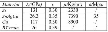
[image:3.595.201.406.508.581.2]and after test is shown in the following Figure.
[image:4.595.137.504.90.229.2]
Fig 4 The plat of chip and bumps Fig 5 The plat of chip and bumps before applying force after applying 6N force
[image:4.595.206.403.271.400.2]According to the experiment, we can obtain the data before and after applying bonding force, which is shown in Table 2 and Table 3.
Table 2 The height of bumps before applying force(µm)
Times
[image:4.595.257.357.354.399.2]region 1 2 3 4 205 205 201 6 203 200 198
Table 3 The height of bumps after applying 6N force (µm)
Times
region 1 2 3 4 199 198 197 6 200 198 198
Analyzing the data in the tables, we get the average deformation of the bumps in applied force is 3.667µm.
Because of the bonding force in the experiment is selected according to the actual process condition, so we have not conducted the experiment in other force. But in the simulation analysis, we chose different bonding force and obtain the deformation of bumps in different bonding force.
Simulation analysis
The simulation analysis is carried out by using ANSYS Workbench14.5. And in the simulation process, we apply different bonding force on the chip, so that we can observe the deformation of the bumps in different condition. The specific parameters are shown in Table 4 (the diameter of bumps is 0.267 mm, h=0.200 mm).
Table 4 The deformation of bumps in different bonding force
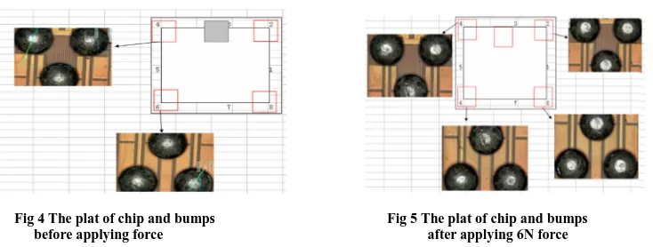
F(N) 6 10 15 50 100 200
∆(µm) 2.925 6.413 10.789 41.339 84.909 171.96
Fig 6 The curve of bumps deformation in different bonding force
Fig 7 The simulation image of bumps deformation in different bonding force
In the figure 7,the black frame represents initial position of the chip, the changing position of the chip represents the bumps deformation
3.2 Chip stress analysis
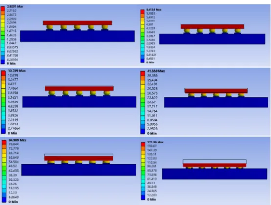
In the process of flip chip bonding, the chip is brittle material, and it is easy to happen brittle fracture if the stress in the chip is too large[8]. In the simulation process of the bonding force, the size of the chip model is 3×3×0.2mm.According to the stress in the chip, we can get a range of the bonding force, which the chip will not be damaged. In the case of applying different bonding force, the stress in the chip is shown in table 5.
Table 5 The stress in the chip in different bonding force
F(N) 6 10 15 50 100 200
σ(MPa) 4.545 8.182 12.743 44.41 90.433 184.39
According to the simulation result, we make a curve of the chip stress in different force, which is shown in Figure 8. From the curve trend in the Figure, we can conclude that the stress in the chip is increasing with the increasing bonding force. If the crack length of the chip is 2c, according to the Griffith fracture formula
= ( ) =( ) ( ) , we can calculate and obtain the critical stressσ0.Comparingthe stress in the chip with
the critical stress, we can judge whether the chip will be broken.
0 50 100 150 200
0 6 10 15 50 100 200
d
ef
o
rm
at
io
n
(
µ
m
)
[image:5.595.176.453.227.437.2]Fig 8 The curve of stress in the chip in different bonding force
Fig 9 The simulation image of stress in the chip in different bonding force
From the Figure 9, we can see that the distribution of the stress in the chip is relatively uniform, the stress will be larger at the location of the bumps, which is dangerous point.
CONCLUSION
The flip chip bonding is the mainstream semiconductor packaging process at present, although it is used widely, its theoretical research is rarely. Based on the stress strength theory and fracture mechanics theory, and combined with experimental and simulation analysis, this paper studies the bumps deformation and the stress in the chip in the bonding process, which provides theoretical basis and reference for the practical work.
Acknowledgements
This work was financially supported by the Beijing Nova Program No.Z151100000315079. Especially, the authors would like to thank the 45th Research Institute of CETC for help in doing the experiment.
REFERENCES
[1]Soonwan Chung; Zhenming Tang; Seungbae Park.Transactions on Advanced Packaging, IEEE,2007,30(1),38-43. [2]Rozalia Beica. Microelectronics Packaging Conference (EMPC),2013,1-4.
[3] Paul S H; Wang C P; Ding G T. Microelectron Reliab, 2004, 44(1), 719-737.
[4]Fuliang Wang; Lei Han; Jue Zhong. International Conference on Electronic Packaging Technology(ICEPT),
2006,1-4.
[5] Libres; J. Arroyo; J.C.Electronic Components and Technology Conference (ECTC),2010,1-4.
[6]Mercado; Lei L; Sarihan.Transactions on Components and Packaging Technologies, IEEE,2003,26(4),719-723.
4.545 8.182 12.743 44.41
90.433 184.39
0 50 100 150 200
0 6 10 15 50 100 200
st
re
ss
(M
P
a)
[image:6.595.194.434.231.469.2][7]Yang D G; Ernst L J; Hof C V. Microelectron Reliab,2000, 40,1533-1538.
[8] Chengjie Jiang; Jia Xi; Fei Xiao; Chuanguo Dou.International Conference onElectronic Packaging Technology