Three-state dual spin valve structure
B. S. Chun*, C. Fowley, M. Abid and J.M.D. Coey
School of Physics and CRANN, Trinity College, Dublin, Ireland.
Abstract
A dual spin valve is built with exchange bias on the top and bottom pinned layers and a central
free layer. By suitable choice of the antiferromagnetic and ferromagnetic layer thicknesses, it is
possible to separate the three magnetization switching fields and produce a staircase
magnetoresistive curve. The maximum magnetoresistance ratio is 7.6% for
current-perpendicular-to-plane and 6.3% for current-in-plane geometries with intermediate
magnetoresistances of 3.9% and 3.0% respectively. The use of exchange bias in a multistate
memory device is discussed.
Keywords: Giant magnetoresistance, dual spin valve, exchange bias, multistate memory
PACS Numbers: 75.47.De
* Present address: Department of Materials Science and Engineering, Moscow, Idaho, United
States of America.
1. Introduction
Spin valve structures have found applications in high density read heads, programmable logic
devices, and nonvolatile magnetic random access memory (MRAM) applications.1-4 The basic
layer5. There are two limiting magnetic configurations in such a device, where the ferromagnetic
layers are aligned parallel or antiparallel, which corresponds to a low and high resistance state
respectively. One of the ferromagnetic layers is often coupled to an adjacent antiferromagnetic
layer which provides exchange bias so that its hysteresis loop is not centered at zero field but is
offset by a field of 10 – 100 mT. This is the ‘pinned’ layer, whereas the other ferromagnetic
layer is ‘free’, as its magnetization will switch around zero field. The spin-polarized current
through the conducting spacer layer depends on the relative orientation of the magnetic moments
of the electrodes. The giant magnetoresistance (GMR) ratio in a spin valve with a conducting
spacer layer is defined as (RAP–RP)/RP, where RP and RAP are the resistances when the
magnetizations of the two ferromagnetic layers are aligned parallel and antiparallel, respectively.
Accordingly, one bit of binary information can be stored in a SV cell which switches between
these two states.
The principal advantage of magnetic random access memory over conventional semiconductor
random access memory is nonvolatility. The growing interest of magnetic random access
memory has arisen from the large magnetoresistive signals that were predicted6,7 and later
observed8-10 in magnetic tunnel junctions with crystalline MgO barrier layers. The possibility of
spin-torque-transfer (STT) magnetization switching11 in these structures12 where data is written
by passing a spin-polarized current through a thin magnetic layer, which is the free layer in a
spin valve structure, has also generated interest in these devices. Unlike half-select MRAM,13
create an Oersted field to switch the free layer element between parallel and antiparallel states,
STT switching remains effective as the device dimensions are scaled down. In the Oersted field
switching scheme, a larger current density in the bit and word lines is needed to write a bit as the
device dimensions are reduced. The amount of information that can be stored in a cell can also
be increased, making use of the third spatial dimension. This may be done in a vertical shift
register, the magnetic ‘racetrack’ memory.14
Another approach is to increase the number of discrete memory states that can be stored in
resistance states of the cell. Binary memory states currently dominate but multistate memory has
been receiving much attention, because it offers excellent storage density. 15-17 Although the
possibility of fabricating a multistate magnetic device has been demonstrated, these devices, are
however, hard to adapt for practical use because of the inability to selectively switch single
elements in a multi-level stack. In a half-select MRAM switching scheme, the field from bit and
word lines disturbs more than one element in the stack. Multilevel switching by STT has been
demonstrated in an MTJ with a two domain free layer.18 Microwave assisted switching has been
proposed and allows for selective switching of embedded elements19, but it is reliant on the
spin-torque-oscillator20which is not yet a fully practical proposition.
Here, we take a different approach by using a dual spin valve (DSV) structure with
current-in-plane (CIP) or current-perpendicular-to-current-in-plane (CPP) geometry to create a multistate memory cell.
The main point of the DSV structure is that the free layer shows completely independently
resulting in three resistance states.21,22 The multiple states are achieved by controlling the
exchange coupling between both ferromagnetic pinned layers and the adjacent antiferromagnetic
pinning layers.
2. Experimental Methods
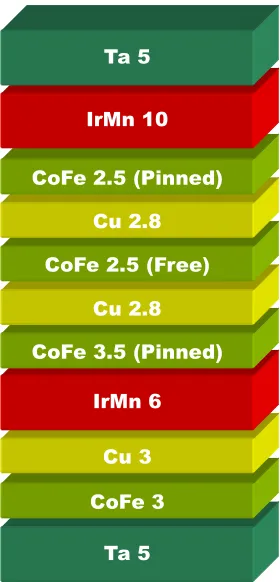
The dual spin valve was of the form; Si/SiO2/Buffer/IrMn 6/CoFe 3.5/Cu 2.8/CoFe 2.5/Cu
2.8/CoFe 2.5/IrMn 10/Cap (thickness in nm). The buffer layer was Ta 5/CoFe 3/Cu 3. The
capping layer was Ta 5. The stack is shown in Fig. 1. Target compositions were Co90Fe10 and
Ir22Mn78 in atomic percent. Samples were prepared using a Sputtered Films Inc. ‘Shamrock’
deposition tool with a typical base pressure of less than 3×10⁻⁹ mbar. The free and pinned layer
easy axes were aligned along the same direction by applying a 10 mT magnetic field during
deposition. Post deposition annealing was carried outex-situat 250°C in a 5×10⁻⁸ mbar vacuum
under an applied field of 800 mT for 2 hours. A probe station with an electromagnet capable of
generating a magnetic field of ± 180 mT was used to measure the magnetoresistive properties of
the dual spin valves. CIP measurements were carried out using a standard 4-point probe
technique in a linear geometry. Lateral sample size was approx 20 mm x 20 mm, and inter-probe
distance was less than 5 mm. A current of 1 mA, applied parallel to the field, was used to probe
the resistance as a function of applied magnetic field. CPP measurements were carried out on
nanopillar samples fabricated by electron beam lithography in a FEI Dual Beam system
operating at 30 kV. Devices of 250 nm x 400 nm were fabricated using TOK negative e-beam
insulate the top and bottom contacts. A top contact of Ta 5/Ag 50/Ta 5 was deposited by
sputtering and subsequent lift off. The magnetic properties of the dual spin valve structure were
characterized by using a Quantum Design Superconducting Quantum Interference Device
magnetometer (SQUID).
3. Results and Discussion
Before implementing the dual spin valve, we characterized the exchange bias and
magnetoresistance (MR) of single spin valve structures with one free and one pinned
ferromagnetic layer, with either top or bottom pinning, as a function of layer thickness. To check
the antiferromagnetic layer thickness dependence of exchange bias and MR, we made SiO2/Ta
5/NiFe 3.5/CoFe 5/Cu 2.8/CoFe 3.5/IrMn t/Ta 5 (nm) and SiO2/Ta 5/CoFe 3/Cu 3/IrMn t/CoFe
3.5/Cu 2.8/CoFe 5/Ta 5 (nm) stacks for the top and bottom pinning, respectively. Also, to check
the ferromagnetic layer thickness dependence of exchange bias and MR ratio, we made SiO2/Ta
5/NiFe 3.5/CoFe 5/Cu 2.8/CoFe t/IrMn 10/Ta 5 (nm) and SiO2/Ta 5/CoFe 3/Cu 3/IrMn 6/CoFe
t/Cu 2.8/CoFe 5/Ta 5 (nm) top and bottom pinned stacks, respectively.
Fig. 2 (a) shows the antiferromagnetic thickness dependence of the exchange bias and MR
ratio. Below a 4 nm thickness of antiferromagnetic IrMn, there is no effective exchange bias.
The exchange bias appears at an antiferromagnetic layer thickness of 4 nm and it continues to
increase up to a maximum at a layer thickness of 6 nm or 10 nm, where it reaches a value of 46
mT and 31 mT for bottom or top pinning, respectively. Beyond the maxima, the exchange bias
antiferromagnetic layer thickness is similar to work previously reported.23 Exchange bias results
from an interfacial interaction between the ferromagnetic and the antiferromagnetic layer. This
may be influenced by crystal structure,25magnetic domains,26antiferromagnetic grain size23, and
interface roughness.24 The authors of Ref. 23 the authors explain a curve very similar to that in
Fig 2 (a) in terms of a model where the exchange bias depends critically on the antiferromagnetic
IrMn grain size. The smallest antiferromagnetic particles are not blocked and do not contribute to
the exchange bias, the axis of the largest particles cannot be set because the anisotropy energy is
too great and it is only IrMn particles with a grain of 8-10 nm which are effective for exchange
bias.
The main reason for larger exchange bias in bottom pinned structures than top pinned
structures, is the enhancement of the texture, grain size and morphology of the subsequent layers
associated with using the CoFe and Cu buffer layer.26 The exchange bias field is inversely
proportional to the ferromagnetic layer thickness in both cases, as shown in Fig. 2 (b).
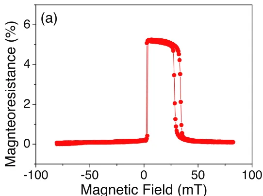
Examples of the magnetoresistance curves for top pinned and bottom pinned structures are
shown in Figure 3, all measurements are made in the CIP geometry. Fig. 3 (a) and (b) show data
for an optimized top pinned device with CoFe 2.5/IrMn 10 (nm) and bottom pinned device with
an IrMn 6/CoFe 3.5 (nm), respectively.
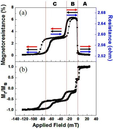
Results on the dual spin valve structure are shown in Fig. 4, the thickness of the two
ferromagnetic CoFe pinned layers and the antiferromagnetic IrMn pinning layers are chosen to
states with different resistance values. Fig. 4 (a) shows the MR curve measured in the CIP
geometry, and the magnetization switching of each layer can be clearly distinguished. This is
because the free layer switching near zero field to provide a high resistance state, and the two
pinned layers switching at different applied reverse fields. In order to give a clear picture of the
magnetic moment configurations, the magnetization direction of each magnetic layer is
represented by coloured arrows in the figure. The red, black, and blue arrows indicate the
magnetization direction of the top pinned, free and bottom pinned CoFe layers, respectively.
Starting from the positive saturation field, the magnetization directions of all layers are parallel
to the applied field, which results in minimum resistance. As the negative field is increased to
near 3 mT, the resistance dramatically increases, because the magnetization direction of the
central free layer reverses to an antiparallel orientation with respect to that of both pinned layers,
resulting in the maximum resistance. As the negative field is increased to near 20 mT, the
magnetization direction of the top pinned CoFe layer starts to reverse and is aligned parallel with
free layer but antiparallel to the bottom pinned CoFe layer, resulting in an intermediate resistance.
Since the bottom pinned CoFe layer has higher exchange bias than that of the top pinned CoFe
layer, which was characterized in Fig. 2, tuning of the exchange coupling strength to give well
separated switching fields for both pinned layers is possible. This allows the intermediate
resistance state to be stable in field regardless of whether the sweep is started from positive or
negative saturation field. By further increasing applied magnetic field beyond 60 mT, the
respect to that of the free and top pinned CoFe layer and resulting again in the low resistance
state.
For clarity the three magnetoresistance states which could potentially give three states at zero
field are labeled A, B and C in Fig. 4 (a). A, B, and C can be thought of as corresponding to “0”,
“1” and “2” in terms of memory storage. Since the intermediate state at point C is only stable in
an applied field this device cannot function as a three state memory. In order to function as a
memory device all three states (“0”, “1”, and “2”) must normally be stable in zero field.
Fig. 4 (b) shows the magnetization curves of the dual spin valve structure as a function of the
applied magnetic field along the easy axis. The magnetization switching characteristics agrees
well with the resistance results in Fig. 4 (a). There is one extra switch visible in the
magnetization curve, compared to Fig. 4 (a), at near zero field. This results from magnetization
switching of CoFe buffer layer just above Ta seed layer. The GMR effect results from spin
dependent scattering of the conduction electrons in the bulk and/or at the interface of the facing
pairs of ferromagnetic layers. The CoFe underlayer does have any influence on the GMR.
Results obtained for the dual spin valve in the CPP geometry in a 250 nm x 400 nm nanopillar
are shown in Fig. 5. As can be seen from the figure, in the CPP configuration the CPP-GMR
ratio increased from 6.3% to 7.6% and the resistance value decreased from 2.7 ohm to 0.93
compared to the CIP configuration. The higher GMR ratio in CPP configuration is related to the
fact that the spin diffusion length is the important parameter in this geometry, and the electrons
important parameter is the mean free path of conduction electrons since current is shunted by the
normal metal layer, which cannot contribute to GMR. The thicker the nonmagnetic spacer, the
lower the GMR. The small resistance value results from the much smaller active volume that is
probed using the CPP geometry. Switching by spin-torque-transfer should also be possible in the
CPP geometry but our pillar was too large to observe it. The main advantage of the CPP
geometry is that the GMR ratio increases with decreasing cell size.
Although multiple resistance states are achieved in our device by optimizing the exchange
coupling between the two ferromagnetic pinned layers and the two antiferromagnetic pinning
layers, the structure in its present form cannot operate as a multibit memory, because only two of
the three states are stable in zero magnetic field. The intermediate resistance state is only
accessible in an applied field. Even if the two pinned layers were pinned in opposite directions,
there would only be two storage states, corresponding to the two orientations of the free layer. In
order to achieve multilevel storage in this type of structure, at least one of the antiferromagnetic
pinning layers has to be removed. It has previously been demonstrated, using three free layers
with differing coercivities, that a multilevel memory can be constructed without exchange
pinning.12 If just one of the pinning layers is removed, we have a dual spin valve with two free
layers, one half of the device making an exchange biased spin valve, and the other half making a
pseudo spin valve with two switchable layers with different coercivity. Provided the
magnetoresistance is different for the two halves, the device has four different resistance states in
spin valve is 3% and that the pseudo spin valve is 6%, the device exhibits a staircase of four
resistance states according to the previous magnetic field history of the structure. The value of
the resistance states being determined by parallel and series resistance laws for CIP and CPP
geometries, respectively.
4. Conclusions
We have built a dual spin valve structure with distinct switching fields for the two pinned
layers, which is a device with a staircase of three distinct magnetoresistive states. The multiple
resistance states are achieved by controlling the exchange coupling between both two
ferromagnetic pinned layers and adjacent antiferromagnetic pinning layers. As it stands, the
structure no application as a multibit since the intermediate resistance state is only available in an
applied field. However, if either of the top or bottom pinned layer is unpinned, it would switch
about zero with the free layer, and a four-state dual spin valve structure can be achieved.
Acknowledgements
This work was supported by Science Foundation Ireland as part of the MANSE project. One
author (M. Abid) received a Marie Curie Institutional Fellowship at CRANN. We are grateful to
References
1. Prinz, G.A., Magnetoelectronics,Science282, 1660–1663 (1998).
2. Wolf, S.A., Awschalom, D.D., Burhman, R.A., Daughton, J.M., von Molnar, S.,
Chtchelkanova, A.Y., Treger, D.M., Spintronics: A spin-based electronics vision for the
future,Science294, 1488–1495 (2001).
3. Moodera, J.S., LeClair, P., A quantum leap,Nature Materials,2, 707–708 (2003).
4. Ney, A., Pampuch, C., Koch, R., Ploog, K.H., Programmable computing with a single
magnetoresistive element,Nature425, 485–487 (2003).
5. Dieny, B., Speriosu, V.S., Gurney, B.A., Parkin, S.S.P., Wilhoit, D.R., Roche, K.P., Metin, S.,
Peterson, D.T., Nadimi, S., Spin Valve Effect in soft ferromagnetic sandwiches, Journal of
Magnetism and Magnetic Materials,93, 101 (1991).
6. Butler, W.H., Zhang, X.G., Schulthess, T.C., MacLaren, J.M., Spin-dependent tunneling
conductance of Fe/MgO/Fe sandwiches,Physical Review B, 63, 054416 (2001).
7. Mathon, J., Umerski, A., Theory of tunneling magnetoresistance of an epitaxial
Fe/MgO/Fe(001) junction,Physical Review B,63, 220403 (2001).
8. Parkin, S.S.P., Kaiser, C., Panchula, A. Rice, P.M., Hughes, B., Samant, M., Yang, S.-H.,
Giant tunnelling magnetoresistance at room temperature with MgO (100) tunnel barriers,
Nature Materials,3, 862-867 (2004).
9. Ikeda, S., Hayakawa, J., Ashizawa, Y., Lee, Y. M., Miura, K., Hasegawa, H., Tsunoda, M.,
diffusion in CoFeB/MgO/CoFeB pseudo-spin-valves annealed at high temperature, Applied
Physics Letters,93, 082508 (2008).
10. Slonczewski, J.C., Current-driven excitation of magnetic multilayers, Journal of Magnetism
and Magnetic Materials,159, L1-L7 (1996).
11. Diao, Z., Li, Z., Wang, S., Ding, Y., Panchula, A., Chen, E., Wang, L.-C., Huai, Y.,
Spin-transfer torque switching in magnetic tunnel junctions and spin-Spin-transfer torque random
access memory,Journal of Physics: Condensed Matter,19, 165209-165021 (2007).
12. Jeong, W.C., Lee, B.I., Joo, S.K., Three level, six state multilevel magnetoresistive RAM
(MRAM),Journal of Applied Physics,85, 4782-4784 (1999).
13. Dave, R.W., Steiner, G., Slaughter, J.M., Sun, J.J., Craigo, B., Pietambaram, S., Smith, K.,
Grynkewich, G., DeHerrera, M., Akerman, J., Tehrani, S., MgO-based tunnel junction
material for high-speed toggle magnetic random access memory, IEEE Transactions on
Magnetics,42, 1935-1939 (2006).
14. Parkin, S.S.P., Hayashi, M., Thomas, L., Magnetic domain-wall racetrack memory, Science
320, 190 (2008).
15. Zheng, Y.K., Wu, Y.H., Guo, Z.B., Han, G.C., Li, K.B., Qiu, J.J., Xie, H., Luo, P., Multistate
per-cell magnetoresistive random-access memory written at Curie point, IEEE Transactions
on Magnetics,38, 2850-2852 (2002).
16. Lim, C.K., Kim, Y.S, Park, N.Y., Lee, J., Multibit MRAM using a pair of memory cells,
17. Ventura, J., Pereira, A.M., Arujo, J.P., Zhang, Z., Liu, Y., Freitas, P.P., Three-state memory
combining resistive and magnetic switching using tunnel junctions, Journal of Physics D:
Applied Physics40, 5819-5823 (2007).
18. Lou. X., Goa, Z., Dimitrov, D.V., Tang, M.X., Demonstration of multilevel cell spin transfer
switching in MgO magnetic tunnel junctions,Applied Physics Letters,93, 242502 (2008).
19. Zhu, J-G., Zhu, X., Tang, Y., Microwave Assisted Magnetic Recording, IEEE Transactions
on Magnetics,44, pg 125 (2008).
20. Devolder, T., Meftah, A., Ito, K., Katine, J.A., Spin transfer oscillators emitting microwave
in zero applied magnetic field,Journal of Applied Physics,101,063916 (2007).
21. Childress. J.R., Carey, M.J., Cyrille, M.-C., Carey, K., Smith, N., Katine, J.A., Boone, T.D.,
Driskill-Smith, A.A.G., Maat, S., Mackay, K., Tsang, C.H.,Fabrication and recording Study
of All-Metal Dual-Spin-Valve CPP Read Heads, IEEE Transactions on Magnetics,42, 2444
(2006).
22. Law, R., Tan, E.-L., Sbiaa, R., Liew, T., Chong, T.C., Reduction in critical current for spin
transfer switching in perpendicular anisotropy spin valves using an in-plane spin polarizer,
Applied Physics Letters,94, 062516 (2009).
23. Vallejo-Fernandez, G., Fernandez-Outon, L.E. and O’Grady, K., Antiferromagnetic grain
volume effects in metallic polycrystalline exchange bias systems, Journal of Physics D:
Applied Physics,41, 112001 (2008).
Antiferromagnetic layer thickness dependence of the IrMn/Co exchange-bias system,
Physical Review B,68, 214420 (2003).
25. Takano, K., Kodama, R.H., Berkowitz, A.E., Cao, W., Thomas, G., Interfacial
Uncompensated Antiferromagnetic Spins: Role in unidirectional anisotropy in
polycrystalline Ni81Fe19/CoO bilayers,Physical Review Letters,79, 1130-1133 (1997).
26. Nogués, J., Lederman, D., Large exchange bias and its connection to interface structure in
FeF2–Fe bilayers,Applied Physics Letters,68, 3186-3188 (1996).
27. Yagami, K., Tsunoda, M., Takahashi. M., Enhancement of exchange bias in MnIr/CoFe
based spin valves with an ultrathin Cu underlayer and in situ MnIr surface modification,
Figure 1 The dual spin valve stack.
Ta 5 CoFe 3
Cu 3 IrMn 6 CoFe 3.5 (Pinned)
Cu 2.8 CoFe 2.5 (Free)
Cu 2.8 CoFe 2.5 (Pinned)
Figure 2. Variation of the exchange bias and magnetoresistive values (a) with antiferromagnetic
layer thickness for a fixed ferromagnetic thickness of 3.5 nm and (b) with ferromagnetic layer
thickness for a fixed antiferromagnetic layer thickness of 10 nm in the case of top pinning and 6
nm in the case of bottom pinning. In each panel, data are included for both top and bottom
-100 -50 0 50 100 0 2 4 6
M
a
g
n
te
o
re
si
s
ta
n
c
e
(%
)
Magnetic Field (mT)
(a)
SiO
2 / Buffer / CoFe 5 / Cu 2.8 /CoFe 2.5 / IrMn 10/ Cap
-100 -50 0 50 100
0 2 4 6
SiO2/ Buffer /IrMn 6 / CoFe 3.5/ Cu 2.8 / CoFe 5 / Cap
(b)
M
a
g
n
te
o
re
si
s
ta
n
c
e
(%
)
[image:17.595.163.434.117.319.2]Magnetic Field (mT)
Figure 3. Examples of magnetoresistance curves for optimized a) top-pinned and b) bottom
Figure 4. (a) The MR curve with current-in-plane (CIP) geometry and (b) M-H curve. Both
curves show the stability of the intermediate state in field (sectioned as C). The extra switch near
zero field in (b) but not in (a) is due to the presence of CoFe 3 nm in the buffer layer which does
[image:18.595.114.494.63.497.2]Figures 5. Resistance value and MR curve for the dual spin valve measured in CPP GMR. The