N A N O E X P R E S S
Open Access
Field modulation in Na-incorporated Cu(In,Ga)Se
2
(CIGS) polycrystalline films influenced by
alloy-hardening and pair-annihilation probabilities
Yonkil Jeong
1†, Chae-Woong Kim
2†, Dong-Won Park
1, Seung Chul Jung
2, Jongjin Lee
1and Hee-Sang Shim
1*Abstract
The influence of Na on Cu(In,Ga)Se2(CIGS) solar cells was investigated. A gradient profile of the Na in the CIGS absorber layer can induce an electric field modulation and significantly strengthen the back surface field effect. This field modulation originates from a grain growth model introduced by a combination of alloy-hardening and pair-annihilation probabilities, wherein the Cu supply and Na diffusion together screen the driving force of the grain boundary motion (GBM) by alloy hardening, which indicates a specific GBM pinning by Cu and Na. The pair annihilation between the ubiquitously evolving GBMs has a coincident probability with the alloy-hardening event. PACS:88. 40. H-, 81. 10. Aj, 81. 40. Cd,
Keywords:Cu(In,Ga)Se2, solar cells, grain growth model, alloy hardening, pair-annihilation
Introduction
Thin film solar cells are promising candidates for power generation and other integrated photovoltaic applica-tions, as part of an effort to develop new renewable energy technologies [1,2]. Specifically, chalcopyrite semi-conductor systems, such as Cu(In,Ga)Se2 (CIGS), have
attracted a great deal of interest as potential absorber materials for thin film solar cells. In recent years, the CIGS solar cells have demonstrated efficiencies of greater than 20% using three-stage co-evaporation meth-ods [3]. One of the common methmeth-ods for improving the performance of CIGS solar cells uses soda-lime glass (SLG) substrates, in which the amount of Na incorpo-rated into the CIGS absorber layer is on the order of 0.1 at.% [4,5]. Several models have been proposed that explain the effect of Na on device performance. Wang et al. reported that the carrier concentration in the CIGS absorber layer increases due to a reduction in the amount of compensating (In,Ga)Cudefects due to the
substitution with NaCu[6-8]. In contrast, Herberholz et
al. suggest that the existence range ofa-CuInSe2 widens
due to the incorporation of 0.1 at.% of Na, which sup-presses the formation of the b-phase [9]. Rockett sug-gests that Na incorporation leads to an increase in the grain size and the lowest energy surfaces, such as Se-ter-minated (112) surfaces, due to an increase in the atomic mobility during CIGS growth and at grain boundaries [10,11]. Based on ab initio calculations, Persson and Zunger demonstrate that NaCu defects or NaInSe2
phases at grain boundaries decrease the valence-band (VB) maximum due to a lack of Na d-electron states, which is similar to the case of (2VCu + InCu) neutral
defect complexes at grain boundaries [12,13]. However, the dominant phenomenon is an increase in the output voltage from the perspective of CIGS device physics, and an increase in the grain size from a crystallographic perspective. These increases are being recognized as far more acceptable explanations for the improvement in performance.
In this paper, we discuss how an increase in the fill factor is caused by the back surface field (BSF) effect from the perspective of CIGS device physics, and a structural change in the grain size from a crystallo-graphic approach using a combination of alloy-harden-ing and pair-annihilation events.
* Correspondence: [email protected]
†Contributed equally
1Research Institute for Solar and Sustainable Energies (RISE), Gwangju Institute of Science and Technology (GIST), 261 Cheomdan-gwagiro, Buk-gu, Gwangju 500-712, South Korea
Full list of author information is available at the end of the article
Experimental
Fabrication of CIGS absorber film and device
CIGS solar cells were fabricated on Corning glass (CG) and SLG substrates. The basic properties, including the coefficient of thermal expansion (CTE), are summarized in Table 1 for the SLG and the CG [14] (http://www. abrisatechnologies.com). The polycrystalline CIGS films were deposited on Mo-coated SLG and CG using a typi-cal three-stage co-evaporation process, as described in other studies [15,16]. In the first stage, indium (In), gal-lium (Ga), and selenium (Se) sources were evaporated at a growth temperature of 350°C to form a (In,Ga)2Se3
layer with a thickness of 1μm. In the second stage, cop-per (Cu) and Se were evaporated and reacted with the (In,Ga)2Se3 layer at a temperature of 550°C to form the
Cu-rich phase. In the third stage, In, Ga, and Se were evaporated to form the Cu-poor phase, while maintain-ing the substrate temperature. Then, CdS buffer and i-ZnO/Al:ZnO window layers were sequentially deposited. The cell area was defined as 0.49 cm2 using a simple mechanical scribing tool.
Characterization
The microstructure of the CIGS absorber layers was investigated using transmission electron microscopy (TEM, JEOL, Tokyo, Japan) operated at an acceleration voltage of 200 keV. The samples were prepared using a dual focused ion beam (FIB) system. Depth profiling of the chemical composition in both device structures was performed with a secondary ion mass spectrometer (SIMS, in a Cameca IMS 4f system, CAMECA SAS, Gennevilliers Cedex, France) using an impact energy of 7.5 keV and a 200 nA O2+ beam and detecting MCs +
complexes (M = 63Cu, 115In, 69 Ga, 80Se, 23Na, and98Mo). The solar cell efficiencies were measured and recorded using a Keithley 4300 source meter under 100-mW/cm2 irradiation (Oriel® Sol3A™, 450-W solar simulator equipped with an AM 1.5-G filter; Oriel Instruments, Irvine, CA, USA) and an incident-photon-to-electron conversion efficiency measurement system for the wavelength range of 300 to 1,200 nm (QEX7, PV Measurements Inc., Boulder, Colorado, USA).
Results and discussion
Microstructure and photovoltaic performances
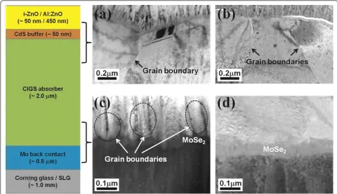
Figure 1 shows the cross-sectional TEM (XTEM) images of the interfaces in the CIGS solar cells on the CG
(Figure 1a,c) and SLG substrates (Figure 1b,d). The solar cells fabricated on the CG and the SLG substrates will be referred to as Na-restricted and Na-incorporated devices, respectively. The interfaces in Figure 1c,d have a quasi-ohmic MoSe2layer formed by the inter-diffusion
of Se and Mo atoms [17,18]. In Figure 1a,b, the grain configurations, such as the size and crystallographic orientation, seem to be similar to one another, while the bottom regions of the CIGS absorber layers in Figure 1c,d clearly show different features. The interface con-figuration in Figure 1c might be that of the elongated grain boundary motion (GBM) between the CIGS poly-crystalline grain blocks, moving toward the Mo surface.
Figure 2 shows the illuminated J-V and external quan-tum efficiency (EQE) curves of the Na-restricted and Na-incorporated devices. The open-circuit voltage (Voc),
short-circuit current density (Jsc), fill factor (FF), and
photo-conversion efficiency (Eff) are summarized in Table 2. The EQE curves exhibit similar absorption band-edges, which represent a very small difference in the output voltage, as shown in Figure 2b. From the EQE in the wavelength range of 400 nm to approxi-mately 550 nm and 600 nm to approxiapproxi-mately 850 nm in Figure 2b, the slightly higher quantum efficiency of the Na-incorporated device leads an improvement in theJsc.
However, the main source of efficiency improvement, which increases significantly from 10.9% to 14.6%, is caused by the enhancement in the FF of greater than 10%. This result could be attributed to the BSF induced at the bottom region of the CIGS absorber layer. The BSF effect might not be from the energy band-gap tun-ing by the In and Ga profile modulation but instead from the energy-level pinning caused by a structural change in the Na-incorporated CIGS absorber layer.
Compositional profile
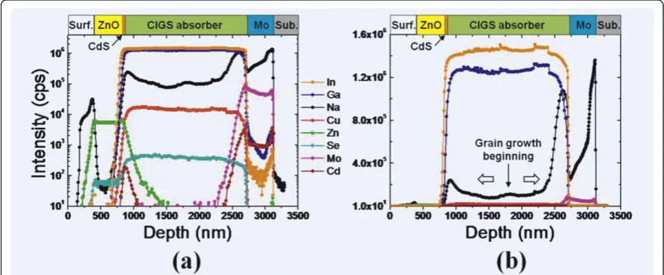
[image:2.595.57.539.100.152.2]Figure 3 shows the SIMS profile plotted on a logarithm and linear scale for the Na-incorporated device as a function of the sputter-etch time (the SIMS profile of the Na-restricted device is not shown in here). The Na is distributed from the substrate to the surface: the Na intensity is higher than that of Cu and Se in the CIGS absorber layer, whereas it is lower than that of In and Ga (Figure 3a). In particular, the gradient of the Na pro-file changes abruptly at the interface between CIGS and Mo. This finding implies two possible diffusion mechan-isms of elemental Na. First, the Na continuously diffuses Table 1 CTE and chemical composition of soda-lime glass and Corning glass substrates
Type CTE (×10-6/°C) Chemical contents (%)
SiO2 Na2O Others
Soda-lime glass 8.4 (in the range of 25°C to approximately 513°C) 72.6 13.9 13.5 Corning glass 4.2 (in the range of 25°C to approximately 671°C) 69.0 1.0 30.0
Jeonget al.Nanoscale Research Letters2011,6:581 http://www.nanoscalereslett.com/content/6/1/581
through the Mo from the SLG during the CIGS grain growth, in which Na diffusion is gradually restricted by the compact CIGS grain blocks, and consequently, Na accumulation is more prominent in the bottom region of the CIGS absorber layer. Second, the Na diffusion should already be in progress during the deposition of the (In,Ga)2Se3 precursor film, and in the beginning of
the CIGS grain growth, Na should begin to spread out upward and downward, as shown in Figure 3b. At the same time, the continuous Na diffusion from the sub-strate results in a prominent Na profile in the bottom
region. In practice, such a Na profile could improve the device performance, as reported in the literature [19]. As far as the Na diffusion mechanism is concerned, the second mechanism seems to be a far more acceptable explanation. Herein, we suggest a model describing a structural change in the CIGS polycrystalline film.
Grain growth model
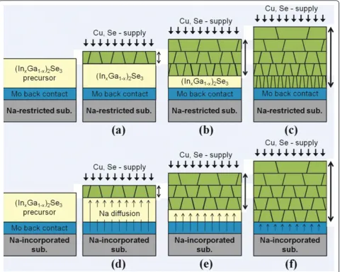
[image:3.595.56.537.89.365.2]Figure 4 provides a detailed schematic of the struc-tural change that occurs during the growth process of the CIGS film for the Na-restricted device (Figure a,b,
Figure 2J-V and EQE curves.(a)Illuminated J-V and(b)EQE curves of Na-restricted and Na-incorporated devices.
Figure 1XTEM images of each interface.(a)the interface between the CdS buffer;(b)the CIGS absorber layers for the Na-restricted device and the Na-incorporated device; the interface between the CIGS absorber layers and the Mo back contact layers for(c)the Na-restricted device;
[image:3.595.58.539.566.715.2]c) and the Na-incorporated device (Figure d,e,f). The (InxGa1-x)2Se3 precursor film is formed in the first
deposition stage of the CIGS film. For the second stage in which Cu and Se are introduced, the grain growth of the CIGS starts from the surface of the (InxGa1-x)2Se3 film (Figure 4a,d). The grain growth
and volume expansion of the CIGS crystal would pro-gress simultaneously upward and downward, leading the GBM. The upward grain growth from the initially formed surface grain results from alloy-hardening and pair-annihilation events in both devices [20-22]. The constant Cu supply to the surface leads to a lower activation energy for the GBM [23,24] because the supplied Cu atoms induce an alloy hardening in the CIGS film and make the upward propagation of the grain boundary more energetically unfavorable. In addition, Cu could act as a driving force screen for the GBM, which indicates that the GBM is partially pinned by the Cu supply. Subsequently, the grain boundaries come together in the same growth direc-tion and are eventually pair-annihilated. The grain size at the top region of the CIGS films, as shown in Fig-ure 1a,b, can be explained by the upward structural evolution. However, the downward structural evolu-tion occurs in a different manner in the Na-restricted and the Na-incorporated devices. In the case of the Na-restricted film, the downward grain growth is accompanied by a volume expansion that weakens the
grain size effect because the Cu diffusion is gradually restricted due to the compactly preformed CIGS crys-tal grains. Finally, the polycryscrys-talline CIGS film is formed as shown in Figure 4c, which is attributed to the structural configuration of the bottom region in Figure 1c. In the Na-incorporated film, the downward grain growth should be the same as that of the Na-restricted device. However, there is sufficient Na diffu-sion from the SLG such that the Cu vacancies are compensated due to the limited diffusion rate of Cu and it maintains grain growth by alloy hardening. Such a structural feature of the bottom region (Figure 4f) is in good agreement with the TEM image, as shown in Figure 1d. It should be noted that the Na diffusion from the SLG occurs during the second stage due to a higher CTE of the SLG substrate, while the Corning glass substrate restricts the Na diffusion due to its lower CTE and lower Na content. From the SIMS profile, we observe that the Na is prominently located at the interface between the CIGS absorber and the Mo back contact, in which the Na might occupy the Cu vacancies or replace the Cu atoms and form Na(In,Ga)Se2 phases, which produces a decrease
in the valence-band maximum at the grain boundaries [12,13]. In other words, the electric field is modulated because the valence-band maximum approaches the Fermi-energy level. Specifically, the prominent Na profile in the bottom region of the CIGS absorber layer is likely to cause energy-level pinning, which could strengthen the BSF.
Conclusions
[image:4.595.56.291.100.139.2]We fabricated Na-restricted and Na-incorporated CIGS solar cells to investigate the influence of Na on the Table 2 Parameters obtained from illuminated J-V curves.
Device Voc(V) Jsc(mA cm-2) FF (%) Eff (%)
[image:4.595.56.539.512.712.2]Na restricted 0.626 30.4 57.1 10.9 Na incorporated 0.641 32.0 71.1 14.6
Figure 3SIMS depth profile. Plotted on (a) a logarithm scale and(b)a linear scale for the Na-incorporated devices.
Jeonget al.Nanoscale Research Letters2011,6:581 http://www.nanoscalereslett.com/content/6/1/581
device performances. The enhancement in the output voltage and photocurrent density for the Na-incorpo-rated device was negligible, while the FF revealed a remarkable increase. This finding could be attributed to the strengthening of the BSF by the energy-level pinning in the bottom region of the CIGS absorber layer. The energy-level pinning originates from the proposed grain growth model wherein the Cu supply and the Na diffu-sion both contribute to the grain growth by a combina-tion of alloy-hardening and pair-annihilacombina-tion events that occur between grain boundaries.
Abbreviations
CIGS: Cu(In,Ga)Se2; GBM: grain boundary motion; SLG: soda-lime glass; CG: Corning glass; VB: valence band; BSF: back surface field; CTE: coefficient of thermal expansion; TEM: transmission electron microscopy; FIB: focused ion beam; SIMS: secondary ion mass spectrometer; XTEM: cross-sectional TEM; EQE: external quantum efficiency;Voc: open-circuit voltage;Jsc: short-circuit current; FF: fill factor; Eff: photo-conversion efficiency.
Acknowledgements
This work was supported by the Core Technology Development Program for the Next-generation Solar Cells of Research Institute for Solar and
Sustainable Energies (RISE), GIST.
Author details
1Research Institute for Solar and Sustainable Energies (RISE), Gwangju Institute of Science and Technology (GIST), 261 Cheomdan-gwagiro, Buk-gu, Gwangju 500-712, South Korea2Korea Institute of Industrial Technology, 1110-9 Oryong-dong, Buk-gu, Gwangju 500-757, South Korea
Authors’contributions
YKJ, CWK and HSS designed and drafted the study. CWK fabricated the CIGS absorber films and devices using three-stage co-evaporation technique. YKJ and HSS carried out the characterization of the CIGS devices. DWP and JJL participated in the establishment of the grain growth mechanism for CIGS absorber film during the three-stage evaporation. All authors read and approved the final manuscript.
Competing interests
The authors declare that they have no competing interests.
[image:5.595.59.540.89.473.2]Received: 12 August 2011 Accepted: 7 November 2011 Published: 7 November 2011
References
1. Niki S, Contreras M, Repins I, Kushiya K, Ishizuka S, Matsubara K:CIGS absorbers and processes.Prog Photovolt:Res Appl2010,18:453. 2. Yuan M, Mitzi DB, Liu W, Kellock AJ, Chey SJ, Deline VR:Optimization of
CIGS-based PV device through antimony doping.Chem Mater2010,
22:285.
3. Green MA, Emery K, Hishikawa Y, Warta W:Solar cell efficiency tables (version 37).Prog Photovolt:Res Appl2011,19:84.
4. Braunger D, Hariskos D, Bilger G, Rau U, Schock HW:Influence of sodium on the growth of polycrystalline Cu(In, Ga)Se2 thin films.Thin Solid Films
2000,361-362:161.
5. Rudmann D:Effects of sodium on growth and properties of Cu(In,Ga)Se2
thin films and solar cells.Doctoral ThesisSwiss Federal Institute of Technology; 2004.
6. Niles DW, Ramanathan K, Hasson F, Noufi R, Tielsch BJ, Fulghum JE:Na impurity chemistry in photovoltaic CIGS thin films: investigation with x-ray photoelectron spectroscopy.J Vac Sci Technol A1997,15:3044. 7. Contreras MA, Egaas B, Dippo P, Webb J, Granata J, Ramanathan K, Asher S,
Swartzlander A, Noufi R:On the role of Na and modifications to Cu(In, Ga)Se2absoorber materials using thin MF (M= Na, K, Cs) precursor
layers [solar cells].IEEE Photovoltaic Specialists Conference1997, 359. 8. Stanbery BJ, Chang CH, Anderson TJ:Engineered phase inhomogeneity
for CIS device optimization.Proc 11th Int Conf on Ternary and Multinary
CompoundsSalford; 1997, 915-922.
9. Herberholz R, Rau U, Schock HW, Haalboom T, Godecke T, Ernst F, Beilharz C, Benz KW, Cahen D:Phase segregation, Cu migration and junction formation in Cu(In, Ga)Se2.Eur Phys J Appl Phys1999,6:131.
10. Rockett A:The electronic effects of point defects in Cu(InxGa1 -x)Se2.
Thin Solid Films2000,361-362:330.
11. Lammer M, Klemm U, Powalla M:Sodium co-evaporation for low temperature Cu(In, Ga)Se2deposition.Thin Solid Films2001,387:33.
12. Domain C, Laribi S, Taunier S, Guillemoles JF:Ab initiocalculation of intrinsic point defects in CuInSe2.J Phys Chem Solids2003,64:1657.
13. Zhang SB, Wei S-H, Zunger A, Katayama-Yoshida H:Defect physics of the CuInSe2 chalcopyrite semiconductor.Phys Rev B1998,57:9642. 14. Tian L, Dieckmann R:Sodium tracer diffusion in an alkaline-earth
boroaluminosilicate glass.Journal of Non-Crystalline Solids2000,265:36. 15. Schleussner S, Zimmermann U, Wätjen R, Leifer K, Edoff M:Effect of
gallium grading in Cu(In, Ga)Se2solar-cell absorbers produced by
multi-stage coevaporation.Sol Energy Mater Sol Cells2011,95:721. 16. Luque A, Hegedus A:Handbook of Photovoltaic Science and
Engineering.London, John Wiely & Sons Ltd; 2002, 567-611. 17. Abou-Ras D, Kostorz G, Bremaud D, Kalin M, Kurdesau FV, Tiwari AN,
Dobeli M:Formation and characterization of MoSe2for Cu(In,Ga)Se2
based solar cells.Thin Solid Films2005,480-481:433.
18. Kohara N, Nishiwaki S, Hashimoto Y, Negami T, Wada T:Electrical properties of the Cu(In,Ga)Se2/MoSe2/Mo structure.Sol Energy Mater Sol
Cells2001,67:209.
19. Shin YM, Shin DH, Kim JH, Ahn BT:Effect of Na doping using Na2Son the
structure and photovoltaic properties of CIGS solar cells.Curr Appl Phys
2011,11:S59.
20. Jeong Y, Choi H, Suzuki T:Invalidity of graded buffers for InAs grown on GaAs(001)-A comparison between direct and graded-buffer growth.J
Cryst Growth2007,301-302:235.
21. Tachikawa M, Yamaguchi M:Film thickness dependence of dislocation density reduction in GaAs-on-Si substrates.Appl Phys Lett1990,56:484. 22. Sato T, Suzuki T, Tomiya S, Yamada S:Dislocation-limited electron
transport in InSb grown on GaAs(001).Physica B: Cond Matter2006, 376-377:579.
23. Schlenker T, Luis Valero M, Schock HW, Werner JH:Grain growth studies of thin Cu(In, Ga)Se2films.J Cryst Growth2004,264:178.
24. Rudmann D, Bremaud D, Zogg H, Tiwari AN:Na incorporation into Cu(In, Ga)Se2for high-efficiency flexible solar cells on polymer foils.J Appl Phys
2005,97:084903.
doi:10.1186/1556-276X-6-581
Cite this article as:Jeonget al.:Field modulation in Na-incorporated Cu (In,Ga)Se2(CIGS) polycrystalline films influenced by alloy-hardening and pair-annihilation probabilities.Nanoscale Research Letters20116:581.
Submit your manuscript to a
journal and benefi t from:
7Convenient online submission 7Rigorous peer review
7Immediate publication on acceptance 7Open access: articles freely available online 7High visibility within the fi eld
7Retaining the copyright to your article
Submit your next manuscript at 7 springeropen.com
Jeonget al.Nanoscale Research Letters2011,6:581 http://www.nanoscalereslett.com/content/6/1/581