N A N O E X P R E S S
Open Access
Transient surface photovoltage studies of bare
and Ni-filled porous silicon performed in different
ambients
Petra Granitzer
1*, Klemens Rumpf
1, Yuri Strzhemechny
2and Puskar Chapagain
2Abstract
Mesoporous silicon and porous silicon/Ni nanocomposites have been investigated in this work employing light-dark surface photovoltage (SPV) transients to monitor the response of surface charge dynamics to illumination changes. The samples were prepared by anodization of a highlyn-doped silicon wafer and a
subsequent electrodepositing of Ni into the pores. The resulting pores were oriented towards the surface with an
average pore diameter of 60 nm and the thickness of the porous layer of approximately 40μm. SPV was performed
on a bare porous silicon as well as on a Ni-filled porous silicon in vacuum and in different gaseous environments (O2, N2, Ar). A significant difference was observed between the‘light-on’and‘light-off’SPV transients obtained in vacuum and those observed in gaseous ambiences. Such behavior could be explained by the contribution to the charge exchange in gas environments from chemisorbed and physisorbed species at the semiconductor surface.
Keywords:Porous silicon; Electrodeposition; Surface photovoltage PACS:81.05.Rm; 73.20.-r; 75.50.-y; 82.45.Yz
Background
Porous silicon (PS) exhibits numerous properties directly related to its microstructure, which in turn can be modi-fied within a broad range of morphologies. Freshly etched PS offers a hydrogen-terminated surface. Due to the high surface area and the high reactivity, such as-etched PS oxidizes easily. It can be oxidized, e.g., by storing in air (native oxide layer) and via thermal or chemical treatment. Oxidation is the main aging aspect and therefore, know-ledge about the oxidation state of the surface is of import-ance. Light illumination decreases the H-termination of as-etched samples. Photoirradiation in an oxygen ambient causes photo-oxidation at the surface and thus accelerates aging of the material. Chemical stability of PS is one of the preconditions rendering the material compatible with any application for which surface modification is desirable.
For practical applications of PS in solar cells, light-emitting diodes, chemical and gas sensors, etc., it is thus desirable to understand the behavior of PS in different
ambients. The surface of PS is known to be sensitive to the surrounding environments [1-3]. For example, sur-face electronic states could be affected by gas species by physisorption, chemisorption, or desorption from the surface [4,5]. On the other hand, filling of PS with mag-netic metals [6,7] is of interest due to both the distinct properties of the nanosized deposits and the employ-ment of silicon as the base material, key for integration in microtechnology.
In this work, we employed transient surface photovol-tage (SPV) to monitor the response of the surface elec-tronic structure of PS to the change of ambience. SPV probes light-induced variations in the electric potential of a studied surface, mostly in semiconductors and insu-lators [8]. Surface potential barrier in semiconductors is formed due to charges trapped in surface states. The illumination-induced changes of the surface barrier de-pend strongly on the surface/subsurface electronic struc-ture, which, in turn, can be affected by the physisorbed and chemisorbed species. In transient SPV experiments, the surface potential is monitored as a function of illu-mination time which can provide information about the different transport mechanisms in semiconductors. SPV
* Correspondence:[email protected] 1
Institute of Physics, Karl Franzens University Graz, Universitaetsplatz 5, Graz 8010, Austria
Full list of author information is available at the end of the article
is a non-destructive and a highly surface-sensitive tool, which can be operated in different environments. A number of SPV studies on PS were reported in the lit-erature, with most of them performed in ambient air [9-11]. Some authors addressed the influence of the surface chemistry on the SPV response in PS, revealing depend-ence on the microstructure and chemical environment of the surface [12-14]. However, there was insufficient experi-mental evidence of the influence of the surface environ-ment (such as vacuum vs. gas) on the SPV response in PS. To address this, in our work, bare PS specimens as well as samples with embedded Ni deposits have been measured by SPV in vacuum and in different gaseous environments (O2, N2, Ar). It was revealed that the illumination-induced
charge transport mechanisms were strongly influenced by the experimental ambiences. The behavior of the SPV tran-sients obtained for gaseous environment was significantly different from that observed in high vacuum.
Methods
The investigated PS samples were fabricated by anodiza-tion in aqueous hydrofluoric acid soluanodiza-tion. Highly n -doped silicon was used as a substrate. The produced morphology revealed average pore diameters of 60 nm and a thickness of the porous layer of about 40μm as de-termined by the scanning electron microscopy (SEM). Ni-nanostructures were electrochemically deposited within the pores of these templates. The size of the Ni-deposits ranged between 60 and 200 nm, whereas their diameter always correlated with the pore diameter. Figure 1 shows an SEM image of a Ni-filled PS sample with deposits of approximately 100 nm in size. Details of the fabrication process of the PS/Ni nanocomposite can be found in an earlier publication [15]. The light-dark transient SPV was
employed using a broad-spectrum incident white light, which included super-bandgap wavelengths. The surface was first allowed to saturate in light, and then to reach equilibrium in the dark. SPV signal was monitored using the Kelvin probe method, a non-contact technique utilized to measure contact potential difference (CPD) between the sample surface and the probe [8]. Characterization of a bare PS and a Ni-filled PS using SPV transients for dif-ferent environments were performed in high vacuum as well as in O2, N2and Ar.
Results and discussion
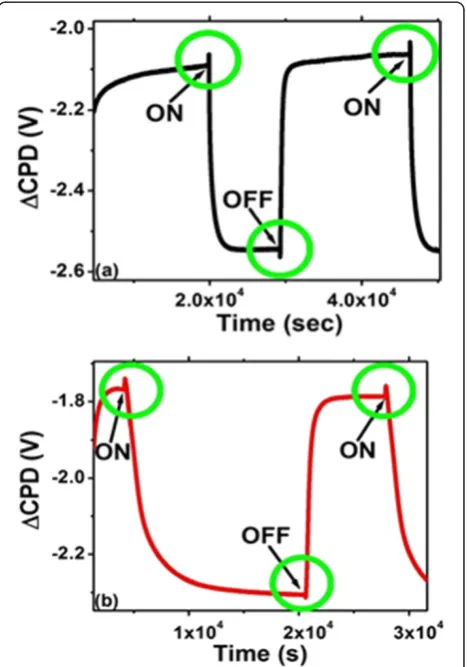
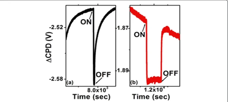
SPV transients for both types of samples in different gases show anomalous spikes of SPV during both‘ light-on’ and ‘light-off’ events (Figure 2). Similar behavior is observed for all three gaseous environments. After obtaining the SPV transients in these gas ambients, the experimental chamber was evacuated and then the SPV transients were obtained in vacuum.
[image:2.595.306.540.370.704.2]As a result, we observed that the PS surface was very sensitive to the experimental ambient, as one can see from
[image:2.595.58.292.525.694.2]Figure 1SEM image of a Ni-filled PS sample.SEM image (formed by back-scattered electrons) of a Ni-filled PS sample with a high density of Ni-particles in the pores with an average size of 100 nm.
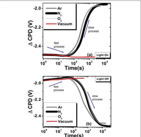
Figure 3. In vacuum, the sharp SPV spikes disappeared whereas the light-on and light-off saturation times became dissimilar. Resolving the SPV transients obtained in gas-eous environments on the logarithmic time scale (cf. Figure 4), one can see that these curves contain both fast and slow components with opposite contributions to charge dynamics. The initial fast process in the case of light-on and light-off events in the gaseous environments occurs over a time scale of tens of seconds, whereas the en-tire event until saturation is in the range of thousands of seconds. However, the transients observed in vacuum re-vealed only one relatively fast process. Since the fast process is always present regardless of the ambient conditions, we believe that it is related to the charge recombination occur-ring in PS. On the other hand, the slow process is present only in the gaseous environments suggesting that it might be related to the non-vacuum ambient.
A detailed discussion of fast and slow SPV transients can be found in ref. [9]. Coexisting slow and fast charge transfer processes were reported for wide-bandgap mate-rials and analyzed theoretically by Reschikov et al. in [16-18], where it was proposed that the fast and slow components arise due to both internal contributions (re-lated to surface/interface states) and external phenom-ena (related to the ambient environment). We suggest that such model could be applicable here considering a thin native oxide layer on the silicon surface. It is likely that physisorption, chemisorption, or desorption of gas species govern the observed charge dynamics. In a gas-eous environment, both the internal and external charge transfer mechanisms occur in PS simultaneously but on different time scales resulting in non-trivial transients. The initial fast process during the light-on transient
could be related to the drift of the illumination-induced electrons in Si towards the bulk and holes towards the Si/oxide interface due to the electric field in the space charge region (cf. [8]). On the other hand, the electrons in the trap states at the interface may recombine with the flux of holes from the Si side leading to the initial decrease of the CPD in the light-on transient. The de-crease in the band bending reduces the depletion width and the barrier height. More electrons can now cross the barrier, tunnel through the oxide layer and become captured by the physisorbed gas species at the free sur-face and convert them into chemisorbed ones. This in-creases the negative charge at the free surface and consequently the band bending yielding a slow increase in the CPD of the light-on transient. However, when similar measurements were performed in vacuum, slow components were absent in transients (Figure 3). We propose that in vacuum, the physisorbed species could be removed from the surface during evacuation. Thus, only the PS internal mechanism would contribute to the SPV transients in vacuum during the light-on process, explaining the observed behavior.
In addition, our experiments show that there is no dif-ference between the SPV transients for the bare and Ni-filled PS. This fact indicates that the metal deposits inside the pores do not influence the optoelectronic transport properties of PS, an important observation considering potential multifunctional (magnetic/chemical/pressure) sensor applications of Ni-filled PS.
Conclusions
[image:3.595.61.539.504.717.2]In this work, employing transient SPV, we studied charge dynamics of mesoporous silicon and Ni-filled mesoporous
silicon in different gas ambients and vacuum. We found that SPV transients for both types of samples in gaseous environments showed a non-trivial behav-ior during the light-on and light-off events. Vacuum transients showed a different behavior without the slow component. The time scale of the light-on and light-off events in vacuum and in gaseous ambients differs by three orders of magnitude. We suggest that the observed behavior is related to the charge ex-change between the silicon/oxide interface and free-surface adsorbates.
Competing interests
The authors declare that they have no competing interests.
Authors’contributions
PG and KR fabricated the porous silicon and Ni-filled porous silicon samples, and PC and YS performed the surface photovoltage transient measurements. All authors discussed the data and prepared the manuscript. All authors read and approved the final manuscript.
Acknowledgements
[image:4.595.62.539.88.549.2]The authors thank the Institute for Electron microscopy at the University of Technology Graz, Austria, for SEM investigations of the samples.
Author details
1
Institute of Physics, Karl Franzens University Graz, Universitaetsplatz 5, Graz 8010, Austria.2Department of Physics and Astronomy, Texas Christian University, 76129 Fort Worth, TX, USA.
Received: 16 May 2014 Accepted: 30 July 2014 Published: 21 August 2014
References
1. Amato G, Boarino L, Bellotti F:On the apparently anomalous response of porous silicon to nitrogen dioxide.Appl Phys Lett2004,85:4409. 2. Rucavado E, Badilla JP, Ramírez-Porras A:The Effect of N2 in Vapor
Detectors Based on Porous Silicon Layers.ECS Trans2008,16:299–303. 3. Peng KQ, Wang X, Lee S-T:Gas sensing properties of single crystalline
porous silicon nanowires.Appl Phys Lett2009,95:243112. 4. Fagila G, Baratto C, Sberveglieri G, Gaburro Z, Pavesi L:Surface
photovoltage studies of porous silicon in presence of polluting gases: toward a selective gas sensor.Proc SPIE2003, 5222. doi:10.1117/12.509074. 5. Skryshevsky VA, Zinchuk VM, Benilov AI, Milovanov YS, Tretyak OV:
Overcharging of porous silicon localized states at gas adsorption.
Semicond Sci Technol2006,21:1605–1608.
6. Granitzer P, Rumpf K, Krenn H:Ferromagnetic nanostructures incorporated in quasi-onedimensional porous silicon channels suitable for magnetic sensor applications.J Nanomater2006,2006:1–7. 7. Granitzer P, Rumpf K, Roca AG, Morales MP, Poelt P, Albu M:Investigation
of a Mesoporous Silicon Based Ferromagnetic Nanocomposite.Nanoscale
Res Lett2010,5:374–378.
8. Kronik L, Shapira Y:Surface photovoltage phenomena: theory, experiments, and applications.Surf Sci Rep1999,37:1–206. 9. Burnstein L, Shapira Y, Partee J, Shinar J, Lubianiker Y, Balberg I:Surface
photovoltage spectroscopy of porous silicon.Phys Rev B1997,55:R1930. 10. Suntao W, Yanhua W, Qihua S:Measurement and analysis of the
characteristic parameters for the porous silicon/silicon using photovoltage spectra.Appl Surf Sci2000,158:268–274.
11. Wang B, Wang D, Zhang L, Li T, Phys J:A comparative study of transition states of porous silicon by surface photovoltage spectroscopy and time-resolved photoluminescence spectroscopy.J Phys Chem Solids1997,
1:25–31.
12. Wang B, Wang D, Zhang L, Li T:Surface photovoltaic characterizations of porous silicon layers.Thin Solids Films1997,293:40–44.
13. Duzhko V, Koch F, Dittrich T:Transient photovoltage and dielectric relaxation time in porous silicon.J Appl Phys2002,91:9432.
14. Dittrich T, Duzhko V:Photovoltage in free-standing mesoporous silicon layers.Phys Status Solidi A2003,197:107.
15. Granitzer P, Rumpf K:Porous silicon–a versatile host material.Materials 2010,3:943.
16. Reschikov MA, Foussekis M, Baski AA:Surface photovoltage in undoped n -type GaN.J Appl Phys2010,107:113535.
17. Foussekis M, Baski AA, Reshchikov MA:Photoadsorption and photodesorption for GaN.Appl Phys Lett2009,94:162116. 18. Reshchikov MA, Sabuktagin S, Johnstone DK, Morkoc H:Transient
photovoltage in GaN as measured by atomic force microscope tip.
J Appl Phys2004,96:2556.
doi:10.1186/1556-276X-9-423
Cite this article as:Granitzeret al.:Transient surface photovoltage studies of bare and Ni-filled porous silicon performed in different ambients.Nanoscale Research Letters20149:423.
Submit your manuscript to a
journal and benefi t from:
7 Convenient online submission
7 Rigorous peer review
7 Immediate publication on acceptance
7 Open access: articles freely available online
7 High visibility within the fi eld
7 Retaining the copyright to your article