N A N O E X P R E S S
Open Access
Altering the Optical Properties of
GaAsSb-Capped InAs Quantum Dots by Means of
InAlAs Interlayers
A. Salhi
1,2*, S. Alshaibani
2, Y. Alaskar
2, H. Albrithen
3, A. Albadri
2, A. Alyamani
2and M. Missous
1Abstract
In this work, we investigate the optical properties of InAs quantum dots (QDs) capped with composite In0.
15Al0.85As/GaAs0.85Sb0.15 strain-reducing layers (SRLs) by means of high-resolution X-ray diffraction (HRXRD) and photoluminescence (PL) spectroscopy at 77 K. Thin In0.15Al0.85As layers with thickness t= 20 Å, 40 Å, and 60 Å were inserted between the QDs and a 60-Å-thick GaAs0.85Sb0.15 layer. The type II emissions observed for GaAs0.85Sb0.15-capped InAs QDs were suppressed by the insertion of the In0.15Al0.85As interlayer. Moreover, the emission wavelength was blueshifted for t= 20 Å and redshifted for t≥40 Å resulting from the increased confinement potential and increased strain, respectively. The ground state and excited state energy separation is increased reaching 106 meV for t= 60 Å compared to 64 meV for the QDs capped with only GaAsSb SRL. In addition, the use of the In0.15Al0.85As layers narrows significantly the QD spectral linewidth from 52 to 35 meV for the samples with 40- and 60-Å-thick In0.15Al0.85As interlayers.
Keywords: Quantum dots, Strain, InAlAs/GaAsSb, III–V semiconductors
Background
In the last decades, self-organized quantum dots (QDs) synthesized using the Stranski–Krastanov technique have attracted a great deal of attention. Their optical and elec-tronic properties have been investigated intensively owing to their potential applications in optoelectronic devices [1]. The widely investigated InAs/GaAs QD system has been employed in a range of optoelectronic devices as ac-tive material. During the growth of these nanostructures, significant change in the size and the shape of the QDs oc-curs during the capping process. This process is quite complex and involves intermixing, segregation, or strain-enhanced diffusion [2]. The use of a pure GaAs capping layer limits the QD emission to less than 1300 nm. To alleviate this issue, strain-reducing layers made of (Ga, In)(As, Sb, N) have been used [2–7]. In particular, the ternary GaAsSb has received particular attention as its resulting band alignment can be tailored to be of type I or
type II by changing the Sb content [8,9] and by its cap-ability in extending the emission wavelength beyond the C-band [10]. However, the difference in energy between the fundamental and excited state is limited to 60–75 meV when GaAsSb is used as a strain-reducing layer (SRL) [11]. This energy separation does not prevent carriers from escaping thermally from the QDs. For applications requiring a long carrier lifetime, the insertion of a thin barrier between the InAs QDs and GaAsSb will be benefi-cial, as it will increase the carrier separation between the QDs and GaAsSb quantum well (QW). As an example, GaAs interlayers have been used resulting in an enhance-ment of solar cell power efficiency by a factor of 23% [12]. The use of InAlAs layers may be of interest to engineering the type of radiative recombination. For type II transition, the insertion of InAlAs will increase the carrier lifetime [13] and the energy separation between the fundamental and first excited states [14–16]. Moreover, the insertion of an InAlAs layer between InAs QDs and GaAsSb is ex-pected to decrease In segregation and suppress In and Ga atoms intermixing between the InAs QDs and the GaAsSb SRL and reduce further the QD strain [17]. InAlAs/ InGaAs composite SRLs have been used to cap InAs QDs
* Correspondence:[email protected]
1
School of Electrical and Electronic Engineering, The University of Manchester, Sackville Street, Manchester M13 9PL, UK
2National Center for Nanotechnology and Advanced Materials, KACST, Riyadh 11442, Saudi Arabia
Full list of author information is available at the end of the article
resulting in long wavelength emission and a favorable en-ergy separation between the fundamental and excited state as high as 104 meV [16,18].
In this paper, we report the first investigation of the ef-fect of using an In0.15Al0.85As interlayer on the optical
properties of InAs/GaAs0.85Sb0.15 QDs by means of
photoluminescence (PL) spectroscopy. In particular, the emission wavelength variation, the type of optical emis-sion, the spectral linewidth, and the energy separation between the fundamental and first excited state were studied in details.
Methods
The samples investigated in the present study were grown on epi-ready quarter 2″ p-type GaAs (001) sub-strates in a Veeco Gen20A Molecular Beam Epitaxy sys-tem. Valved crackers were used to generate As2and Sb2
dimers. Following the growth of a GaAs buffer layer at 590 °C, the substrate temperature was then lowered to ~ 485 °C to grow a nominally 2.5-ML-thick InAs QDs. After a short pause under As2flux, a composite In0.15
A-l0.85As/GaAsSb SRL was deposited immediately followed
by the growth of a 5-nm-thick GaAs at the same temperature after which the growth temperature was in-creased to 570 °C to grow a 38-nm GaAs barrier layer. The thickness of GaAsSb was fixed at 60 Å while the thickness of In0.15Al0.85As was varied from 20 to 60 Å.
The 60-Å-thick GaAsSb SRL was realized by using a As2/Sb2 flux ratio giving a Sb content of 15% as
deter-mined by X-ray diffraction measurements on a reference sample. A fixed Ga growth rate of 0.5ML/s was used for all the layers. Four samples denoted as A, B, C, and D were grown for which the In0.15Al0.85As thickness twas
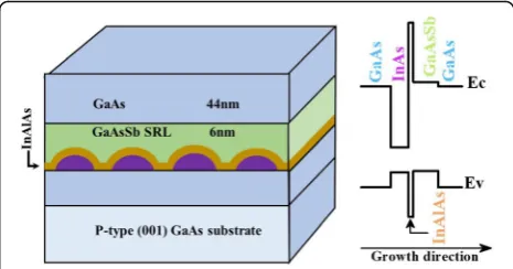
set to 0 Å, 20 Å, 40 Å, and 60 Å, respectively. Based on the procedure used by Krijn [19] and using the parame-ters in [20], the relative position of the conduction and valence bands have been estimated and a schematic of the grown structures with their corresponding band dia-gram are depicted in Fig.1.
The crystal quality of the samples was characterized by high-resolution X-ray diffraction (HRXRD) using a Panalytical X-ray diffractometer. The optical properties of the grown samples were assessed by means of PL spectroscopy at 77 K using a PL module connected to a Vertex 80 Fourier Transform Infrared instrument (Bru-ker Optics GmbH) and using a thermoelectrically cooled high-gain InGaAs detector [21]. The samples were ex-cited with a CW 532-nm solid-state laser source.
Results and Discussion
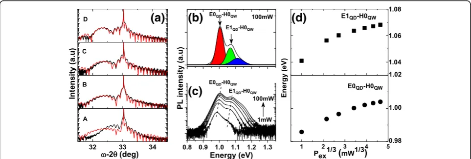
The crystal quality of the grown samples were character-ized by HRXRD using rocking curve scans by recording the diffraction pattern from 004 atomic planes. Figure2a shows the obtained diffraction patterns for samples A, B,
C, and D corresponding to InAlAs thickness of 0, 20, 40, and 60 Å, respectively. Clear satellite peaks resulting from the InAs/InAlAs/GaAsSb are observed showing the good crystal quality of the grown samples. The simu-lated X-ray rocking curves are included in Fig.2a along-side the experimental data. The obtained average Sb content in the reference sample A is 13% and the thick-ness of GaAsSb is 66 Å. These values were used in sam-ples B, C, and D to find the In content and the thickness of the InAlAs interlayer. The simulation showed that the average In content is 13.5% and the thickness of the InAlAs interlayer is 22 Å, 44 Å, and 65 Å in samples B, C, and D, respectively, which are close to the nominal thicknesses.
The optical properties of the reference sample A were investigated first at 77 K using the power-dependent PL technique. Figure2b shows the PL spectrum for an exci-tation power of 100 mW. The PL spectrum can be fitted by three Gaussian peaks centered at 1004 meV, 1068 meV, and 1113 meV, which can be identified as the fun-damental and excited optical transitions. The full width at half maximum (FWHM) of the fundamental and first excited states are 52 and 58 meV, respectively. In order to understand the origin of the observed first two optical transitions, the excitation power was varied from 1 to 100 mW and the corresponding PL spectra were ac-quired as depicted in Fig.2c. For each excitation power, the energy of the first two peaks was extracted using multi-Gaussian function fitting and plotted as a function of the cube root of the excitation power as shown in Fig. 2d. The energy of the fundamental transition de-creases with reducing the excitation power consistent with a type II transition indicating that the emission is a result of the recombination of electrons located in the fundamental electron state in the QD (E0QD) and holes
located in the GaAsSb QW (H0QW). For InAs/GaAsSb
type II band alignment, the localization of electrons and holes in the QDs and GaAsSb SRL, respectively, induces
Fig. 1Schematic of the grown structures and corresponding energy band diagram of InAs QDs capped with a composite In0.15Al0.85As
/GaAs0.85Sb0.15. The In0.15Al0.85As thicknesst= 0 Å, 20 Å, 40 Å, and 60
[image:2.595.305.538.88.210.2]a band-bending effect resulting from the electric field, which is predominantly along the growth direction [22]. The type II transition energy is expected to increase pro-portionally with the third root of the excitation power as demonstrated by Jin et al. [22]. Similarly, the energy of the first excited state transition decreases with reducing the excitation power, and this transition is most likely the result of the recombination of electrons in the first electron excited state in the QD (E1QD) and holes within
the GaAsSb QW (H0QW) as the density of states in the
GaAsSb QW is much larger than the density of states in the QDs. The first two optical transitions are illustrated in Fig. 3a. We note also that the energy separation be-tween the fundamental and first excited state ΔE re-mains nearly constant at 64 meV with decreasing excitation power, and this is evidence that the electric field resulting from the charge build up is perpendicular to the growth direction [22], i.e., the holes in the GaAsSb are localized above the QDs. A type II emission is expected in sample A as the Sb content in the GaAsSb, which is 13%, is close to the composition where a transition from type I to type II occurs [23, 24]. For
the considered Sb content, a small valence band offset between the QDs and the GaAsSb QW should exist fa-voring the localization of holes in the GaAsSb QW and subsequently type II emissions [25,26].
Figure4a shows the PL emission corresponding to the samples with different In0.15Al0.85As thickness with
exci-tation power ranging from 1 to 100 mW. Three main peaks can be identified for all the samples containing an In0.15Al0.85As interlayer. We note an alteration of the
en-ergy peak positions of the different radiative channels with respect to the reference sample A. At an excitation power of 100 mW, the energy of the fundamental transi-tion, FWHM, and the energy separation ΔE were ex-tracted and compared to sample A. The exex-tracted values are reported in Fig.4b.
The ground state transition of sample A occurs at 1004 meV with a FWHM of 52 meV and an energy sep-aration ΔE of 64 meV. Inserting 20 Å of In0.15Al0.85As
(sample B) induces a blueshift of the ground state transi-tion by 52 meV. The blueshift is consistent with what have been observed when a composite InAlAs/InGaAs was used for QDs grown at nearly the same growth
(a)
(b)
(d)
(c)
Fig. 2aHigh-resolutionω/2θscans for samples A, B, C, and D.bPL spectrum of sample A obtained at 77 K and 100 mW excitation.c Power-dependent PL of sample A at 77 K.dThe corresponding energy peak for the first two optical transitions versus Pex1/3at 77 K
(a)
(b)
[image:3.595.57.539.88.251.2] [image:3.595.60.540.569.712.2]temperature [27]. The ground state transition energy blueshift of the InAs QDs in sample B results from the increased confinement potential [15]. As the barrier for electrons and holes are increased, the energy level separ-ation of electrons and holes should increase leading to the observed emission blueshift. It is well known that capping InAs with GaAs results in a reduction of the QD height as a consequence of In segregation and In-Ga intermixing [28]. The introduction of Sb in the GaAs capping layer reduces the QD decomposition by inhibit-ing the strain driven In-Ga intermixinhibit-ing [29]. The inser-tion of the InAlAs interlayer is expected to suppress further the In segregation and In-Ga intermixing result-ing from the inactivity of Al adatoms. In fact, Jun et al. [17] have shown by means of STEM that the use of a InAlAs/InGaAs combination layer as a capping layer strongly suppresses In segregation, and In–Ga intermix-ing along the growth direction durintermix-ing the cappintermix-ing process of the InAs QDs, leading to the increased height of the nanostructures and a higher In concentration in InAs QDs after capping. Considering the low growth temperature of the QDs, i.e., 485 °C, the indium segrega-tion and interface intermixing between the QDs and InAlAs interlayer are expected to be insignificant as a re-sult of the inactivity of Al adatoms.
The FWHM andΔE are reduced and increased to 39 meV and 92 meV, respectively. Increasing further the thickness of In0.15Al0.85As to 40 Å and 60 Å (samples C
and D, respectively) causes a redshift of the emission wavelength. This redshift is probably driven by the modification of the strain in InAs QDs as the total thick-ness of the composite InAlAs/GaAsSb SRL increases with increasing InAlAs thickness [30]. This may change
the structural dimensions of the QDs and hence modify the energy levels of electrons and holes. It seems that for samples C and D (40 Å and 60 Å, respectively), the strain effect dominates the confinement potential effect. The lowest FWHM of 35 meV and the highest energy separ-ationΔE of 35 meV and 106 meV were obtained respect-ively for sample D. The largeΔE is caused by the use of a thicker InAlAs layer and possibly an increased QD height [31, 32]. The energy separation is comparable with that obtained when a composite InAlAs/InGaAs SRL is used (104 meV) [16, 33]. The reduction of the FWHM can be understood in terms of a reduction of intermixing between In0.15Al0.85As and QDs and hence a
preservation of the QD distribution. The extracted pa-rameters are summarized in Table1.
The PL intensity of samples B and C was increased compared to sample A; however, a strong reduction of the PL intensity was observed for sample D, i.e., a reduc-tion by a factor of 5 compared to sample C. The reduced PL intensity results from the reduction of carrier injec-tion from the GaAsSb layer to the QDs. In fact, during illumination, numerous carriers are photogenerated and the insertion of the In0.15Al0.85As interlayer creates a
barrier for carriers and may limit their injection in the QDs. Carriers may transfer to the QDs through a
(a)
(b)
(c)
Fig. 4aPower-dependent PL of the InAs/In0.15Al0.85As/GaAsSb QDs at 77 K.bThe corresponding peak energy, FWHM, andΔE versus InAlAs thickness
[image:4.595.58.538.88.298.2]andcthe variation of the peak energy of optical transition channels as a function of the cube root of the excitation power for samples B, C, and D
Table 1Extracted parameters at 77 K for samples A, B, C, and D
A B C D
InAlAs (Å) 0 20 40 60
Peak energy (meV) 77 K 1004 1056 1043 1035
FWHM (meV) 52 39 35.5 35
[image:4.595.305.540.662.733.2]tunneling process, and the PL intensity is higher for the samples with thinner In0.15Al0.85As barriers [34]. Sample
D showed the lowest PL intensity as the tunneling through the 60 Å In0.15Al0.85As is greatly reduced, and
this is evidenced by the increased PL emission of the GaAsSb QW as shown in Fig. 4a. The reduction of the tunneling process makes favorable and enhances the ra-diative recombination of electrons and holes in the GaAsSb QW.
The main observation from the power-dependent PL at 77 K for samples B, C, and D shown in Fig.4a is the fixed energy positions of the first two peaks with in-creasing excitation power as opposed to what was ob-served in sample A. This is a characteristic of a type I emission where both electrons and holes are localized within the QDs. The first two emission peaks result from the recombination of electrons and holes in the funda-mental and first excited states in the QDs (E0QD-H0QD
and E1QD-H1QD). We believe that the third peak
origi-nates from a type II emission resulting from the recom-bination of electrons within GaAs and holes localized in GaAsSb QW. Indeed, the energy corresponding to this transition increases with increasing excitation power as shown in Fig. 4a and Fig. 4c characteristic of a type II transition. Moreover, we see that its intensity increases with increasing In0.15Al0.85As layer thickness. This is in
agreement with the reduction of the PL intensity of the fundamental transition as a thicker In0.15Al0.85As layer
reduces carriers tunneling from GaAsSb to the QDs and favors the type II emission obtained from the recombin-ation of electrons and holes located in GaAs and GaAsSb, respectively. A schematic of the recombination channels for samples B, C, and D is depicted in Fig. 3b. The suppression of the type II emission can be under-stood as follows. The insertion of a 20-Å In0.15Al0.85As
layer increases the carrier separation between the QDs and GaAsSb QW, and as a result, the electron and hole wavefunction overlap decreases. Moreover, the fact that the Sb content in the GaAsSb content is close to the type I-type II crossover, the In0.15Al0.85As interlayer will
bring the confined level in the QW (H0QW) below the
first quantized level in the QDs (H0QD) as shown in
Fig.3b and hence holes captured in the QW may tunnel through the InAlAs layer making less probable the type II emission. For a thicker In0.15Al0.85As interlayer (40 Å
and 60 Å), the tunneling is further reduced but the elec-tron and hole wavefunction overlap is substantially re-duced favoring the recombination of electrons in GaAs with holes in GaAsSb [13]. The optical transition of InAs/GaAsSb QDs can be tailored to the type of applica-tion requiring either short or long lifetimes. In our study, we have considered a Sb content of 13% in GaAsSb, which is close to the type I to type II transition. The insertion of an InAlAs interlayer suppressed the
type II emission and increased the energy separation be-tween the fundamental and first excited state, which is desirable for applications requiring a short carrier life-time. The present study can also be tailored for applica-tions requiring a long carrier lifetime. In fact, the combination of using a higher Sb content in the GaAsSb layer and the insertion of an InAlAs interlayer is ex-pected to maintain the type II emission for thin InAlAs interlayers while increasing significantly the carrier life-time. At the same time, the increased energy separation between the fundamental and first excited state will re-duce carrier thermal escape.
Conclusion
InAs QDs capped with composite In0.15Al0.85As/
GaAs0.85Sb0.15 SRLs with varying In0.15Al0.85As
thick-nesses were grown and characterized. Our analysis shows that the insertion of an In0.15Al0.85As layer
sup-presses the observed type II emission obtained from InAs/GaAs0.85Sb0.15QDs. Moreover, the emission
wave-length is blueshifted for t= 20 Å and redshifted for t≥ 40 Å resulting from the increased confinement potential and increased strain, respectively. A large energy separ-ationΔE of 106 meV was obtained for the sample with a 60-Å-thick In0.15Al0.85As interlayer. In addition, the
introduction of the In0.15Al0.85As interlayer reduces
sig-nificantly the FWHM from 52 meV reaching a minimum of 35 meV.
Abbreviations
FWHM:Full width at half maximum; HRXRD: High-resolution X-ray diffraction; PL: Photoluminescence; QDs: Quantum dots; QW: Quantum well; SRLs: Strain-reducing layers
Acknowledgements Not applicable.
Funding
The authors are grateful for King Abdulaziz City for Science and Technology for financial support. The authors would also like to extend their gratitude to EPSRC for their support of this work via EPSRC-EP/P006973/1“FUTURE COMPOUND SEMICONDUCTOR MANUFACTURING HUB”.
Availability of Data and Materials
The datasets generated during and/or analyzed during the current study are available from the corresponding author on reasonable request.
Authors’Contributions
AS conceived the idea and designed the growth experiments. AS performed the molecular beam epitaxial growth with the help of SA and YA. SA performed the PL and HRXRD characterization. AS analyzed the data and wrote the manuscript. HB participated in the discussion. AA, AY, and MM supervised the team. All authors read and approved the final manuscript.
Authors’Information Not applicable.
Competing Interests
Publisher’s Note
Springer Nature remains neutral with regard to jurisdictional claims in published maps and institutional affiliations.
Author details
1School of Electrical and Electronic Engineering, The University of Manchester, Sackville Street, Manchester M13 9PL, UK.2National Center for Nanotechnology and Advanced Materials, KACST, Riyadh 11442, Saudi Arabia. 3Department of Physics and Astronomy, College of Sciences and Aramco Laboratory for Applied Sensors Research, KAIN, King Saud University, Riyadh 11451, Saudi Arabia.
Received: 3 November 2018 Accepted: 27 January 2019
References
1. Gazzano O, Solomon GS (2016) Toward optical quantum information processing with quantum dots coupled to microstructures. JOSA B 33(7): C160–CC75.
2. Keizer JG, Ulloa JM, Utrilla AD, Koenraad PM (2014) InAs quantum dot morphology after capping with In, N, Sb alloyed thin films. Appl Phys Lett 104(5):053116.
3. Shimomura K, Kamiya I (2015) Strain engineering of quantum dots for long wavelength emission: photoluminescence from self-assembled InAs quantum dots grown on GaAs (001) at wavelengths over 1.55μm. Appl Phys Lett 106(8):082103.
4. Raino G, Visimberga G, Salhi A, Todaro MT, De Vittorio M, Passaseo A et al (2007) The influence of a continuum background on carrier relaxation in InAs/InGaAs quantum dot. Nanoscale Res Lett 2(10):509–511.
5. Liu WS, Chu TF, Huang TH (2014) Energy band structure tailoring of vertically aligned InAs/GaAsSb quantum dot structure for intermediate-band solar cell application by thermal annealing process. Opt Express 22(25): 30963–30974.
6. Cheng Y, Fukuda M, Whiteside V, Debnath M, Vallely P, Mishima T et al (2016) Investigation of InAs/GaAs1−xSbxquantum dots for applications in
intermediate band solar cells. Sol Energ Mat Sol C. 147:94–100. 7. Salhi A, Alshaibani S, Alaskar Y, Albrithen H, Albedri A, Alyamani A (2018)
Strain-engineering of GaInAsSb overgrown layers and its effects on the optical properties of InAs/GaAs quantum dots. Opt Mater 79:200–205. 8. Hospodková A, Zíková M, Pangrác J, Oswald J, Kubištová J, Kuldová K et al
(2013) Type I–type II band alignment of a GaAsSb/InAs/GaAs quantum dot heterostructure influenced by dot size and strain-reducing layer composition. J Phys D Appl Phys 46(9):095103.
9. Ulloa JM, Llorens JM, del Moral M, Bozkurt M, Koenraad PM, Hierro A (2012) Analysis of the modified optical properties and band structure of GaAs 1-xSbx-capped InAs/GaAs quantum dots. J Appl Phys 112(7):074311.
10. Salhi A, Alshaibani S, Alaskar Y, Albadri A, Alyamani A (2019) Achieving wavelength emission beyond the C-band from type-II InAs-GaAsSb quantum dots grown monolithically on silicon substrate. J Alloy Compd 771:382–386. 11. Salhi A, Alshaibani S, Alhamdan M, Albrithen H, Alyamani A, El-Desouki M (2017) Effects of Sb incorporation in GaAsSb-capping layer on the optical properties of InAs/GaAs QDs grown by molecular beam epitaxy. Superlattice Microst 101:138–143.
12. Hatch S, Wu J, Sablon K, Lam P, Tang MC, Jiang Q et al (2014) InAs/GaAsSb quantum dot solar cells. Opt Express 22(9):A679–AA85.
13. Kim D, Hatch S, Wu J, Sablon KA, Lam P, Jurczak P et al (2018) Type-II InAs/ GaAsSb quantum dot solar cells with GaAs interlayer. IEEE J Photovoltaics 8(3):741–745.
14. Jia R, Jiang DS, Liu HY, Wei YQ, Xu B, Wang ZG (2002) Influence of combined InAlAs and InGaAs strain-reducing laser on luminescence properties of InAs/GaAs quantum dots. J Cryst Growth 234(2–3):354–358. 15. Liu HY, Sellers IR, Hopkinson M, Harrison CN, Mowbray DJ, Skolnick MS
(2003) Engineering carrier confinement potentials in 1.3-μm InAs/GaAs quantum dots with InAlAs layers: enhancement of the high-temperature photoluminescence intensity. Appl Phys Lett 83(18):3716–3718. 16. Zhang Z, Xu B, Jin P, Meng X, Li CM, Ye X et al (2002) Photoluminescence
study of self-assembled InAs/GaAs quantum dots covered by an InAlAs and InGaAs combination layer. J Appl Phys 92(1):511–514.
17. He J, Wu Y, Wang KL (2010) Structure and composition profile of InAs/GaAs quantum dots capped by an InGaAs and InAlAs combination layer. Nanotechnology 21(25):255705.
18. Liu WS, Chyi JI (2005) Optical properties of InAs quantum dots with InAlAs/ InGaAs composite matrix. J Appl Phys 97(2):024312.
19. Krijn M (1991) Heterojunction band offsets and effective masses in III-V quaternary alloys. Semicond Sci Tech 6(1):27.
20. Vurgaftman I, Meyer J, Ram-Mohan L (2001) Band parameters for III–V compound semiconductors and their alloys. J Appl Phys 89(11):5815–5875. 21. Bruker Optics. Infrared photoluminescence spectroscopy. In: Application Note #
AN134. 2014.https://www.bruker.com/fileadmin/user_upload/8-PDF-Docs/ OpticalSpectrospcopy/FT-IR/VERTEX/AN/AN134_IR_Photoluminescence_EN.pdf. 22. Jin CY, Liu HY, Zhang SY, Jiang Q, Liew SL, Hopkinson M et al (2007) Optical
transitions in type-II InAs/GaAs quantum dots covered by a GaAsSb strain-reducing layer. Appl Phys Lett 91(2):021102
23. Salhi A, Alshaibani S, Alaskar Y, Albadri A, Alyamani A, Missous M (2018) Tuning the optical properties of InAs QDs by means of digitally-alloyed GaAsSb strain reducing layers. Appl Phys Lett 113(10):103101. 24. Ban K-Y, Kuciauskas D, Bremner SP, Honsberg CB (2012) Observation of
band alignment transition in InAs/GaAsSb quantum dots by photoluminescence. J Appl Phys 111(10):104302.
25. Gradkowski K, Ochalski TJ, Williams DP, Healy SB, Tatebayashi J, Balakrishnan G et al (2009) Coulomb effects in type-II Ga(As)Sb quantum dots. Phys. Status Solidi B Basic Solid State Phys. 246(4):752–755.
26. Montes Bajo M, Ulloa JM, del Moral M, Guzman A, Hierro A (2011) Near infrared InAs/GaAsSb quantum dot light emitting diodes. Ieee J Quantum Elect 47(12):1547–1556.
27. Chang KP, Yang SL, Chuu DS, Hsiao RS, Chen JF, Wei L et al (2005) Characterization of self-assembled InAs quantum dots with InAlAs/InGaAs strain-reduced layers by photoluminescence spectroscopy. J Appl Phys 97(8):083511.
28. Utrilla AD, Grossi DF, Reyes DF, Gonzalo A, Braza V, Ben T et al (2018) Size and shape tunability of self-assembled InAs/GaAs nanostructures through the capping rate. Appl Surf Sci 444:260–266.
29. Utrilla AD, Reyes DF, Llorens JM, Artacho I, Ben T, González D et al (2017) Thin GaAsSb capping layers for improved performance of InAs/GaAs quantum dot solar cells. Sol Energ Mat Sol C 159:282–289.
30. Wang P, Chen Q, Wu X, Cao C, Wang S, Gong Q (2016) Detailed study of the influence of InGaAs matrix on the strain reduction in the InAs dot-in-well structure. Nanoscale Res Lett 11(1):119.
31. Chiou R, Kuo DM (2008) Effects of composite InGaAs and InAlAs layers on the emission wavelengths of quantum dots. Chin J Phys 46(3):348–355. 32. Jang Y, Lee H, Lee D, Kim J, Leem J, Noh S (2006) The energy level spacing
from In As∕Ga As quantum dots: Its relation to the emission wavelength, carrier lifetime, and zero dimensionality. J Appl Phys 99:096101.
33. Liu HY, Hopkinson M (2003) Tuning the structural and optical properties of 1.3-μm InAs/GaAs quantum dots by a combined InAlAs and GaAs strained buffer layer. Appl Phys Lett 82(21):3644–3646.