COMPUTER·
DPERATDR'S REFERENCE
HANDBODK
RELATED PUBLICATIONS
The table below lists other publications which may be of interest to the readers of this manual. Unless otherwise indicated by title or footnote, all are maintenance handbooks. Note that maintenance handbooks directly applicable to a particular system are normally supplied with the system.
Title
Handbook of Analog Computation
TR-20 Maintenance Manual
Repetitive Operation Display Units, Models 34.034 and 34.035
Pub"lication Nl.nllber
00 800.0001-3
00 800.2006-0
M226-3
NOTIC E
In order to enable us to process your requests for spare parts and replacement items quickly and efficiently, we request your conformance with the following procedure:
1. Please specify the type number and serial number of the basic unit as well as the EAI part number and de-scription of the part when inquiring about replacement items such as potentiometer assemblies or cups, re-lays, transformers, preciSion resistors, etc.
2. When inquiring about items as servo multipliers, re-solvers, networks, printed circuit assemblies, etc., please specify the serial numbers of the major equip-ment with which the units are to be used, such as: Console, Type 8811, Memory Module, Type 4.204, Serial No. 000, etc. If at all possible, please in-clude the purchase order or the EAI project number under which the equipment was originally procured.
Your cooperation in supplying'the required information will speed the processing of your requests and aid in assuring that the correct items are supplied.
It is the policy nf Electronic Associates, Inc. to supply equipment patterned as closely as possi-ble to the requ':.:rements of the individual customer. This is accomplished, zt'ithout incurring the prohibitive cos:is of custom design, by substituting new components, modifying standard com-ponents, etc., wherever necessary to expedite conformance with requirements. As a result, this instruction;. manual, which has been written to cover standa'rd equipment, may not entirely concur in its cr:Jnte.nt with the equipment,supplied. It is felt, however, that a technically quali-fied person wirJ find the manual a fully adequate guide in understanding, operating, and
main-taining the equ~pment actually supplied.
Electronic Associates, Inc. reserves the right to make changes in design, or to make additions to or improve-ments in its product without imposing any obligation upon itself to install them on products previously manufac-tured.
Printed in U.S.A.
EASTERI, REGION
UNITED STATES AND CANADIAN OPERATIONS
Marketing Division
SALES OFFICE
Eastern Regional Office: West Long Branch. N. J .. Te!: 201·229·1100, TWX 510·239·9208. Telex 01-26655, Cable: PACE West Long Brar.::". N. J.
Special System Department: West Long Branch. N. L Tel: 201·229-1100, TWX 510·239·9208. Telex 01-26655. Cable: PACE West Lon>: Branch, N. J.
Customer Services: West Long Branch. N. J., Tel: 201-229·1100. TWX 510·239-9208. Teiex 01-26655, Cable PACE West Long Branch. 1';. J.
Northeastern District Office: 875 Providence HiJ<hway. Dedham, Massachusetts. Tel: 617-326-6756 SOUTHEASTERN REGION
Southeastern Regional Office: 12260 Wilkins Avenue. Rockville. Maryland, Tel: 301·933-4100 CENTRAL REGION
Central Regional Office: 33166 Des Plaines Ave .. Des Plaines. Illinois, Tel: 312-296-8171 Cleveland District Office: 6741 Ridge Road, Parma, Ohio, Tel: 216-842·1840
SOUTHERN REGION
Southern Regional Office: 3514 Cedar Springs Road, Room 211, Dallas, Texas. Tel: 214-528-4920 Houston District Office: 7007 Gulf Freeway, Room 128, Houston, Texas, Tel: 713·MI-4-3678
Huntsville District Office: Holiday Office Center, Suite 2, 3322 South Memorial Parkway. Huntsville, Ala., Tel: 205·881·7031 WESTERN REGION
Western Regional Office: 1500 East Imperial Highway, EI Segundo, California, Tel: 213·322·3124, TWX 910·348·6284 San Francisco District Office: 4151 Middlefield Road. Palo Alto. California, Tel: 415-321-0363. TWX 910·373-1241
CUSTOMER SERVICES OFFICES EASTERN REGION
Eastern U.S. Headquarters: West Long Branch. N. J .. Tel: 201-229·1100. TWX 510-239-9208. Telex 01-26655. Cable: PACE West Long Branch, N. J.
Northeastern District Office: 875 Providence Highway. Dedham. Massachusetts. Telephone: 617·326-6756 Princeton. New Jersey: U.S. Route No.1. Princeton, New Jersey, P.O. Box 582, Telephone: 609-452·2900 Resident Field Engineers: Bedford. Mass.!Florham Park, N. J./Washington, D.C./Baltimore, Md.!Eatontown, N. J. SOUTHEASTERN REGION
Southeastern Regional Office: 12260 Wilkins Avenue. Rockville. Maryland, Telephone: 301-933-4100 CENTRAL REGION
Central Regional Office: 3166 Des Plaines Ave., Des Plaines. Illinois, Tel: 312-296-8171 Cleveland District Office: 6741 Ridge Road, Parma, Ohio, Telephone: 216-842-1840
Resident Field Engineers: Detroit, Michigan/Pittsburgh, Pennsylvania/Dayton, Ohio/Warren. Michigan SOUTHERN REGION
Southern Regional Office: 3514 Cedar Springs Road. Dallas, Texas. Telephone: 214-528-4920 Houston District Office: 7007 Gulf Freeway, Room 128, Houston. Texas, Telephone: 713-MI 4-3678
HuntSVille District Office: Holiday Office Center. Suite 14, 3322 South Memorial Parkway, Huntsville, Ala., Tel: 205-881-7031 Resident Field Engineers: San Antonio, Texas/Alamogordo, New Mexico/Tulsa, OklahomalHouston. Texas.
WESTERN REGION
Western U.S. Headquarters: CUSTOMER REPAIR FACILITY. 1500 East Imperial Highway, EI Segundo, California, Telephone: 213-322·3220, TWX 910·348-6284
Western U.S. Headquarters: CUSTOMER SERVICES FACILITY, 1500 East Imperial Highway, EI Segundo, California, Tele· phone: 213-322-3220, TWX 910-348-6284
San Francisco District Office: 4151 Middlefield Road, Palo Alto, California, TeleptlOne: 415·321-0363, TWX 910-373-1241 Denver Area: 70 South Benton Drive, Denver, Colorado, Telephone: 303-233-0818
Resident Field Engineers: Edwards, California/Pasadena, California/Moffet Field, California/Douglas Aircraft. Huntington Beach, California
CANADA
Toronto Office: Allan Crawford Associates. Ltd., 65 Martin Ross Avenue, Downsview OntariO, Canada, Tel: 416-636-4910 COMPUTATION CENTERS
Princeton Computation Center: U.S. Route No. 1. Princeton, New Jersey, P.O. Box 582. Tel: 609-452-2900
Los Angeles Computation Center: 1500 East Imperial Highway, EI Segundo, California, Tel: 213-322-3220, TWX 910-348-6284 San Francisco Computation Center: 4151 Middlefield Road, Palo Alto, California, Tel: 415·321-7801. TWX 415-492-9211 Washington. D.C. Computation Center: 12260 Wilkins Avenue, Rockville, Maryland, Tel: 301-933-4100
Research and Computation Division
Research and Computation Division H.adquarters: U.S. Route No. I, Princeton. New Jersey, P.O. Box 582, Tel: 609-452-2900
Engineering and Manufacturing Division
Engineering Department: West Long Branch, N. J .• Tel: 201-229-1100, TWX 510-239-9208. Telex 01-26655, Cable: PACE West
Long Branch. N;. J. .
Manufacturing Ilepartment: West Long Branch, N. J., Tel: 201-229·1100, TWX 510-239·9208, Telex 01-26655. Cable: PACE West Long Brani:h, N. J.
. Other Departments, Divisions and Subsidiaries
Instrument Division: Lon!: BranCh. New Jersey. Tel: 201-229-4400, TWX 510·239·9208, Cable: PACE West Long Branch. N. J. Pacific Data Systems, Inc.: 1058 East First Street, Santa Ana. California. Tel: 714·547·9183, TWX 714·531·0188 Scientific Instruments Department: 4151 Middlefield Road, Palo Alto, California. Tel: 415·321·7801. TWX 910-373·1241
INTERNATIONAL OPERATIONS
SALES & CUSTOMER SERVICES OFFICES UNITED KINGDOM & SCANDINAVIA
Electronic Associates. Ltd.: Burgess Hill, Sussex, England, Tel: Burgess Hill (Sussex) 5101-10, 5201-5, Telex: 87183. Cable: PACE Burgess Hill
BURGESS HILL
Northern Area Office: Roberts House. Manchester Road, Altrincham, Cheshire, Tel: Altrincham 5426 SWEDEN
EAI·Electronic Associates·AB: Hagavagen 14, Solna 3, Sweden, Tel: Stockholm 82-40-96; 82-40·97, Telex Stockholm 10064, Cable: PACE STOCKHOLM
EUROPEAN CONTINENT
EAI-European Continental Regional Office: Centre International, 22nd Floor, Place Rogier. Brussels 1. Belgium. Tel: Brussels 18-40-04, Telex: 2.21·106. Cable: PACEBELG Brussels
FRANCE
EAI-Electronic Associates SARL: 72-74. rue de la Tombe Issoire, Paris '14e, France. Tel: 535.01.07 GERMANY
EAI.Electronic Associates GM8H: 5100 Aachen, Bergdriesch 37, West Germany, Tel: Aachen 2 6042; 26041. Telex 832.676 eai d AUSTRALIA & NEW ZEALAND
EAI-Electronic Associates, Ply .• Ltd.: 26 Albany St., Leonards, N.S.W. Australia, Tel: 43-1557. 43-2705, Cable: PACEAUS, Sydney
Victorian Office: 34 Queens Road, Melbourne S. C. 2. Australia, Tel: 26·1329, Cable: PACEAUS, Melbourne JAPAN
EAI-Electronic Associates, (Japan) Inc.: 9th Mori Building, 1·3 Shiba-Atagocho, Minato-Ku. Tokyo 2, Japan; Tel: 433-4671, Telex: 7814285. Cal'.,,: EAIJAPACE
ENGINEERING AND MANUFACTURING
Electronic Associates. Ltd.: Burgess Hill. Sussex, England, Tel: Burgess Hill (Sussex) 5101-10. 5201·5, Telex: 87183. Cable: PACE BURGESS H:LL
COMPUTATION CENTERS
European Computation Center: Centre International, 22nd Floor, Place Rogier, Brussels 1. Belgium. Tel: Brussels 18-40·04. Telex: 2.21-106. Cat:e: PACE9ElG Brussels
United Kingdom Computation Center: Electronic Associates, Ltd .. Burgess Hill. Sussex, England. Tel: Burgess Hill (Sussex) 5101-10. Telex: 871·183. Cabie: PACE BURGESS HILL
Australian Computation Center: 34 Queens Road, Melbourne S.C. 2. Australia. Tel: 26-1329, Cable: PACEAUS. Melbourne
I
~LECTRONIC
ASSOCIA TES, I NC. West Long Branch, New JerseyADVANCED SYSTEMS ANALYSIS A~D COMPUTATION SERVICES/ANALOG COMPUTERS/DIGITAL COMPUTERS/HYBRID ANALOG-DIGITAL COMPUTATION EQUIPMENTiANALOG AND DIGITAL PLOTTERS/SIMULATION SYSTEMS/SCIENTIFIC AND u.eORATORY INSTRUMENTS/INDUSTRIAL PROCESS CONTROL SYSTEMS I PHOTOGRAMMETRIC EQUIPMENT / RANGE INSTRUMENTA· TlON SYSTEMSITEST AND CHECK-OUT SYSTH'S MILITARY AND INDUSTRIAL RESEARCH AND DEVELOPMENT SERVICES/FIELD ENGINEERING AND EQUIPMENT MAINTENANCE SERVICES.
MANUAL REViSION NOTICE
*
ELECTRONIC ASSOCIATES INC.~
TEM
PAGE
PARA
LONG BRANCH NEW JERSEY
REVISION
Included in the accessory items shipped with each computer is a strip of 100 pressure sensitive labels (EAI 00 342.0572-0). These labels may be attached to the connector blocks to identify the computing components associated with a particular problem.
DATE 3/30/65 MANUAL TITLE TR-20 COMPUTER OPERATORS REViSION NOTICE
NO. 65-13
P l<'k'l<'P k'l\Tr l<' U 1\ l\Tn p'oOJ(
*
THIS MANUAL REVISION NOTICE IS ISSUED TO INCORPORATE IMPROVEMENTS ORCONTENTS (Cont)
6. QUARTER-SQUARE MULTIPLIER ...•••...•.•..• 26
~. General Description ....••.•••.••.•..•...•.••.• ...• 26
b. Multiplication... 26
£. Division. . . • . . • . ••. • . • • . •• . . • • • • • . • . • • 26
7. X2 DIODE FUNCTION GENERATOR •..•.••••.•.••.••••••••••. ,.. 28
a. General Description ..•..•••..•.•....••.•.•...•..•... 28
E..
Generating the Square of an Input Voltage (Single Polarity) ...•..•••...••••..•••..••..•.•.••••• 29Generating the Square of an Input Voltage (Bi-Polar). 29 8. LOG X DFG AND 1/2 LOG X DFG ... 29
a. General Description... 29
E..
Pa tching •...•..•....••.•..•.••...••....•...•••. 329. VARIABLE DIODE FUNCTION GENERATOR GROUPS 2.645 AND 2.713. 32 a. General Description ..•...••.•.•....•...•...•••••• 32
b. Setup Procedure (Fixed Breakpoint VDFG's) ••••••••••• 34
£.
Setup Procedure (Variable Breakpoint VDFG's) ••.••.•. 34 d. Paralleling Fixed Breakpoint VDFG's ...•..•..•...•. 4610. SIGNAL COMPARATORS AND FUNCTION SWITCHES •.•...•••••.•.•. 47
a. Relay Comparator ..•••••••••••.•...•.•••...•.•... 47
b. Electronic Comparator .•• ,... 47
c. Dual Function Switch Group 2.127 ...•...•...••• 50
CONTENTS (Cant)
11. REPETITIVE OPERATION
...
53~. General Description
...
53~. Using Repetitive Operation 54
12. DISPLAY NETWORKS
54APPENDIX I - COMPUTER SYMBOLS
AI-l
APPENDIX II - CIRCUITS USING COMPUTATIONAL COMPONENTS
AII-l
APPENDIX III - AMPLIFIER CIRCUITS FOR SIMULATING TRANSFER
FlJN'CTIONS •••••••••••••••••••• 0 0 • • • • • • • • • • • •
AIII-l
APPENDIX IV - BIBLIOGRAPHY
AIV-l
Figure Number 1. 2. 3.
4.
5. 6.7.
8. 9. 10. 11. 12.13.
14.
15. 16. 17. 18. 19. 20. 21. ILLUSTRATIONS TitleThe TR-20 Desktop Analog Computer with Display Units •• 4
Inserting the Pre-Patch Panel ••••••••..••••••••••••••• 9
The 6.712 Dual DC Amplifier, Showing Use of Bottle
Plug s ... 0 • 0 • • • • • • • • • • • • • • • • • • • • • • • • • • • • • • • • • • • • • • • 1 0 The TR-20 Control Panel 0 • • • • • • • • • • • • • • • 0 • • • • • • • • • • • • • •
Readout Circuit, Simplified Schematics ••••••••••••••••
An At tenua tor •••••••••• ' •••••••••••••••••••••••••••••••
Schematics and Symbols for Attenuators ••••••••••••••••
Operational Amplifier, Simplified Block Diagram
Patching an Amplifier as an Integrator~ Showing Simplified Schematic of an Integrator Network
Patching an Amplifier to a Rep-Op Integrator,
.
... .
Showing Simplified Schematic of Integrator Network .•
Quarter-Square Multiplier Patching
.
... .
Division Circuit for a Quarter-Square Multiplier ••••••
X2 DFG Patching X2 Generating
+
10Patching the Log
.
... .
for -10 ~ X ~ +10 ••••••••••••••••••••
X DFG t s ••••••••••••••••••••••••••••••
VDFG Mounting Locations •••••••••••••••••••••••••••••••
±VDFG Patching •••••••.••••••••••••• e • • • • • • • • • • • • • • • • • • •
Sample Function and Setup Information •••••••••••••••••
Breakpoint Setup Patching
.
... .
+ Variable Breakpoint Diode Function Generator
11
14
18 18 20 23 25 27 30 30 31 32 33 35 36 38SBItlP le Curve s ••• 0 • • • • • • • • • • • • • • • • • • • • • • • • • • • • • • • • • • 40
Breakpoint Location Plot Patching ••••••••••••••••••••• 42
Figure Number
22.
23.
24.
25.
26.
27.
vi
ILLUSTRATIONS (Cont)
Title
Function Setup Patching
.
... .
44Relay Comparator, Simplified Diagrams and Setup
Patching . . . . 48
40.538 Electronic Comparator Unit
.
... .
49Comparator Unit, Functional Block Diagram 51
Electronic Switch Unit, Functional Block Diagram 52
CHAPTER I
INTRODUCTION
Many problems encountered in scientific or engineering work involve mathematical equations or sets of equations whose solution in most cases is difficult or
practi-cally impossible to obtain by the classical approach to equation solution. The TR-20
Analog Computer provides the technical worker with a general purpose computer which permits the rapid solution of linear or non-linear equations.
Although the analog machine is correctly termed a computer, i t does not perform its computations by serial calculations as does the desk calculator or digital computer. Instead i t performs the required mathematical operations in a parallel manner on
con-tinuous variables. In the TR-20, as in most modern analog computers, the continuous
variables are direct current voltages. The electronic analog computer makes i t
pos-sible to build an electrical model of a physical system, where the voltages on the
computer represent the dependent variables of the physical system. Except for a
constant of proportionality, or scale factor, each voltage will behave with time in
a manner similar to the physical system variable. Thus, if the vertical position
of the center of gravity of an automobile oscillates with time during a disturbance, then the voltage representing the height of the center of gravity above the surface will also oscillate; if the temperature of the coolant at the exhaust port of a con-denser rises exponentially to a steady value, then so will the voltage representing i t on the computer.
I t can be said that the actual system and the electrical mode~ are analogous in
that the variables which demonstrate their characteristics ar~ described by relations
which are mathematically equivalent. The actual system has thus been simulated
because of the similarity of operation of the electrical model and the physical
system. This capability of the analog computer is of great value in performing
scientific research or engineering design calculations because i t permits an in-sight into the relationship between the mathematical equations and the response
of the physical system. Once the electrical model is completed, well-controlled
experiments can be performed quickly, inexpensively, and with great flexibility to predict the behavior of the primary physical system.
Although the analog computer utilizes electronic components in its operation, i t is not essential that the user have an extensive knowledge of electrical circuits. The TR-20 is basically a set of mathematical building blocks, each able to perform specific mathematical operations on direct voltages and capable of being easily
interconnected. By appropriately interconnecting these building blocks, an
elec-trical model is produced in which the voltages at the outputs of the blocks obey the relations given in the mathematical description of a physical problem.
Since our interest is frequently in the dynamic behavior of physical systems, the mathematical equations are usually differential equations having time as the
in-dependent variable. In order to solve such equations, the standard components of the computer must perform the following operations: inversion, algebraic summation, integration with respect to time, multiplication and division, and function generation.
The sequence of steps for constructing a dynamic model on an analog computer requires first a mathematical description of the physical system, usually in equation form. From this description the operator derives the information necessary to set up a computer program for interconnecting the computing components and determines the required initial conditions and forcing functions. The computing components are
interconnected with wires called patch cords. The input and output terminations of the computing components are brought out to a patch bay which is usually fitted with a removable Pre-Patch Panel so that patching may be accomplished away from the com-puter. The problem is placed on the computer by inserting the patch panel and
ad-justing the problem parameters to the value of the first case to be investigated. Selected voltages are applied to various components in the form of inputs or initial conditions. These voltages are derived from a precise reference voltage.
Once the computing elements have been patched, adjusted, and energized, the computer is switched into the operate mode. The.voltages on the computer change with time in accordance with the equations that govern the physical system variables. The
be-havior of the computer model is viewed through an output device such as an X-Y plotter, oscilloscope, strip-chart recorder, or digital voltmeter.
This TR-20 Reference Handbook has been prepared to serve as a working guide to the analog programmer or computer operator. The information contained presupposes a knowledge of the analog computer, its basic principles of operation, and programming procedures. (Instructional information in these areas can be obtained from "Basics of Analog Computer Programming" by the
EAr
Education and Training Group.) Reaaersinterestea in more detailed circuit information are referred to the TR-20 Maintenance ·Manual.
CHAPTER II
THE TR- 20 COMPUTER AND COMPUTING COMPONENTS
1. GENERAL DESCRIPTION
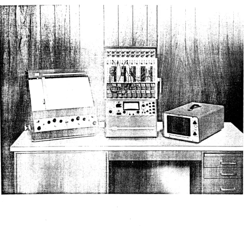
The PACE® TR-20 (Figure 1) is a general purpose analog computer composed of solid-state computing components. The TR-20 is compact in size and is able to operate with stability and precision in a normal office or classroom environment. Reliable, with simplicity in functional design, the TR-20 is easy to use and can be a powerful aid to the individual engineer in the rapid solution of scientific and engineering prob-lems.
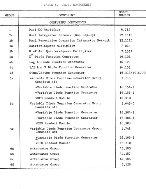
Table I lists the currently available computing components and accessories for the TR-20. The TR-20 utilizes a building block concept, in which individual computing components may be easily interconnected to solve the required equations by forming electronic models analogous to the system under study_ Each building block, either individually or in combination with others, is capable of performing one or more mathematical operations. The computing components in the TR-20 occupy the area
above the slanting control panel area. This area is divided into three rows; the top row contains the coefficient attenuators; the middle row houses the integrator networks, comparators, and other non-linear computing components; the bottom row
provides space for twenty (10 dual units) operational amplifiers. The computing components are constructed on plug-in chassis, and the front of each computing com-ponent consists of a color-coded plastic patching block that contains the input and output terminations for the unit. The computing components are inter-connected by placing patch cords or bottle plugs between the appropriate input and output ter-minations. Most TR-20's are equipped with a removable pre-patch panel that allows
problem patching away from the computer. The pre-patch panel consists of a rigid aluminum frame with individual rows that contain patching blocks identical with the patching blocks that form the front panels of the components. Contact between the pre-patch panel and the computing components is accomplished by means of gold-plated contact springs.
Below the patching area is the monitoring and control panel area which contains con-trols and components that permit (a) switching the computer on and off, (b) mode control of the computer, and (c) measuring statioriary problem voltages. A hinged cover plate directly below the control panel covers the amplifier balancing potenti-ometers and the variable diode function generators.
2. OPERATING CONSIDERATIONS
The TR-20 is completely tested and calibrated at the time of manufacture and is shipped with all components in place. ~fter perform!gg_tl1e-pr~e_l~t!llinar,y-chJ~_c::k-g.p'!
procedure outlined in the TR-20 Maintenance Manual,..>. the c0IIl:puter is ready for
op~r-a-tIo~':--'----' ~"--- ~-
. .--- --...,..
---~..
---.,~-.----.-.. - ... ,
It should be noted that the low voltage levels used in the TR-20 eliminate any shock hazard to the operator when patching components with the computer turned on. Current-limiting circuits protect the reference supplies from damage during short-term over-loading if they are inadvertantly patched to ground or to each other. A patching con-nection that is dangerous to a component usually triggers the overload alarm system.
Figure 1. The TR-20 Desktop Analog Computer with Display Units
GROUP 1 2a 2b 3a 3b 4a 4b 4c 4d 5a 5b 5c 6a 6b 6c 6d
TABLE I. TR-20 COMPONENTS
COMPONENT
COMPUTING COMPONENTS
Dual DC Amplifier
Dual Integrator Network (Non Rep-Op)
Dual Repetitive Operation Integrator Network
Quarter-Square Multiplier
Bi-Po1ar Quarter-Square Multiplier
X2 Diode Function Generator
Log X Diode Function Generator
1/2 Log X Diode Function Generator
Sine/Cosine Function Generator
Variable Diode Function Generator Group Consists of:
-Variable Diode Function Generator
+Variab1e Diode Function Generato~
VDFG Readout Module
Variable Diode Function Generator Group Consists of:
+Variab1e Diode Function Generator
-Variable Diode Function Generator
VDFG Readout Module
Variable Diode Function Generator Group Consists of:
+Variab1e Diode Function Generator
VDFG Readout Module
Attenuator Group
Attenuator Group
Attenuator Group
Attenuator Group
[image:14.626.65.567.87.738.2]GROUP
7a
7b
Tc
8a 8b
9
10
11
12
6
COMPONENT
COMPUTING COMPONENTS (Cont)
Consists of:
Attenuator Panel
Readout Module
Reference Network
Tiepoint Network
Dual Function Switch Group
Consists of:
Function Switch Assembly
Readout Module
Relay Comparator
Electronic Comparator
POWER AND REFERENCE SUPPLIES
Regulated Power Supply
Reference Regulator
Dual DC Amplifier
OPTIONAL COMPONENTS AND ACCESSORY EQUIPMENT
Repetitive Operation Expansion Group Consists of:
High Speed Repetitive Operation Control Panel
Repetitive Operation Timing Unit
Dual Repetitive Operation Integrator Networks
MODEL NUMBER
42. 185
12.265
12.266
12.267
2.127
20.366
12.264
6.143
40.538
10.179
43.037
6.282
2.246
20.532
36.082
GROUP
13
14
15
16
17
18
19
20
21
22
1
2
COMPONENT
OPTIONAL COMPONENTS AND ACCESSORY EQUIPMENT
Display Unit**
Reactor Kinetics Group
Transport Delay Simulator
Audio Overload Alarm
S lave Cable
Patching Kit
Service Shelf
AC Power Cable
Pre-Patch Panel
Rep-Op Slave Panel
AUXILIARY EQUIPMENT
VARIPLOTTER®
Repetitive Operation Display Unit
MODEL NUMBER
12.987
2.475*
2.448*
13.017
510.038
100.007
51.039
51.040
5 .. 235
20.567
1110*
The operator should be familiar with the following paragraphs before attempting to use the computer·.
*These Components described in separate manuals.
**This Component not required if the Electronic Comparator, Model 40.538 is provided.
a. Insertion of the Pre-Patch Panel
Before inserting the pre-patch panel, the operator should verify that the patch blocks on the pre-patch panel are aligned in the same order as the computing components. Hold the pre-patch panel at a slight angle and place i t in the patch bay groove;
see Figure 2. Move the pre-patch panel to th~ right until i t contacts the
right-hand side of the patch bay. Gently, push the pre-patch panel forward until i t is
flush with the computer. Turn the locking lever down; the pre-patch panel will
slide to the left.
To remove the pre-patch panel, apply a light pressure to the panel to keep i t from falling forward when dis-engaged, and lift the locking lever.
b. Feedback for the Amplifiers
All operational amplifiers should be provided with feedback whenever the computer is turned on. Bottle plugs, connected as shown in Figure 3a, provide feedback and prepare the amplifiers for use as standard inverters or summers.
c. Application of Power
Connect the computer line cord to a receptacle following the precautions given in
the TR-20 Maintenance Manual, and place the OFF-ON switch to the ON position. Place
the RESET-HOLD-OPER switch to the RESET ~osition. Initially, the amplifier
load alarm system will be triggered due to transients; after a few seconds, the over-load indication should cease.
d. Amplifier Balance
Under normal circumstances, the amplifiers will remain balanced for periods of weeks.
However, at intervals i t is desirable to check this condition. If an amplifier is
found to be unbalanced, an adjustment should be made. If the check indicates that
the amplifier balance is rithin tolerance, no adjustment is necessary.
The amplifier must have some sort of feedback in order to be balanced. Normally,
this requirement is satisfied by the circuit in which the amplifier is used. The
amplifier may be balanced while normal inputs are applied. Each amplifier has a
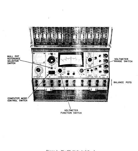
balance potentiometer located behind a hinged cover plate below the Control Panel
(Figure 4). The balance controls are labeled with the number of the amplifier they
serve. To set a balance control, proceed as follows:
(1) Place the computer in the reset mode. Place the VoltmetEr Function
switch in the BAL position. Rotate the AMPL SEL switch to the number of the
ampli-fier to be balanced.
(2) Vary the appropriate Amplifier Balance control until the Vokmeter
reads within two or three divisions of zero. (The amplifier overload alarm system
may be triggered during the balancing process.)
l-I
Figure 2. Inserting the Pre-Patch Panel
10
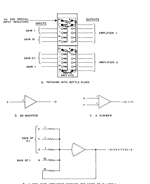
SJ FOR SPECIAL OUTPUTS
INPUT RESISTORS
INPUTS
Z
GAIN
GAIN 10
GAIN 0.1
GAIN I
1[>
b. AN INVERTER
GAIN OF 0.1
{
{
{
y
AMPLIFIER I
10 10
AMPLIFIER 2
10
O. PATCHING WITH BOTTLE PLUGS
X
:[>
-Z -(X +y)
y
C. A SUMMER
Z -O.I(X+Y+Z)-A
GAIN OF I A 10 .
[image:19.615.60.551.82.684.2]d. A HIGH -GAIN AMPLIFIER PATCHED FOR GAINS OF 0.1 AND I
NULL POT REFERENCE SELECTOR SWITCH
[image:20.615.64.546.182.707.2]VOLTMETER FUNCTION SWITCH
Figure 4. The TR-20 Control Panel
VOLTMETER ANGE SWITCH
\fuen the computer is first turned on, a check of amplifier balance will show de-flections that are slightly high, but they will return to normal levels after a
warm-up period. For unusual problems that might be especially sensitive to
ampli-fier unbalance or integrator drift, the ampliampli-fier can be balanced at more frequent intervals in order to keep the meter deflection below one division.
e. Overloads
The computer is equipped with an overload alarm system that indicates the presence of an overloaded amplifier. The visual overload alarm is located on the left side
of the control panel. The lamps are illuminated whenever their associated
ampli-fier is overloaded. Lamps 1 to 20 serve the 20 operational amplifiers; lamps 21
and 22 serve the amplifiers associated with the plus and minus reference amplifiers
respectively. The computer may be equipped with an audio overload alarm that is
located in the rear of the cabinet; it sounds an audible alarm when an amplifier is overloaded.
The overload alarm system indicates that something is wrong with the problem patching,
the problem operation, or the computing components. Usually, no harm is done to
.the equipment by short-term overloads, unless they are caused by excessively high
voltages other than those normally obtainable from the computer itself. However,
several other reasons exist for clearing overloads soon after they are noticed.
(1) If an overload is indicated for amplifier 21 or 22, the value of the
plus or minus reference voltage may be other than ~10.00 volts, adversely affecting
problem solution. An overload in either of these amplifiers generally indicates
a patching error, and should not be allowed to continue over an extended period of time.
(2) Overload of unassigned arnpiifiers does not damage the amplifiers or
affect the problem solution. However, the fact that one or more overload lamps are
lit, however, may cause the operator to overlook an overload occurring in an assigned amplifier, thus causing an erroneous problem solution and defeating the purpose of the alarm system.
3. READOUT FACILITIES AND MANUAL MODE CONTROLS
The operating controls for the readout and mode control circuits are grouped on the sloping control panel area below the computing component cradles as shown in
Figure 4. The functions of the controls are:
Control
Power ON-OFF Switch, S4
Mode Control Switch, SS
Voltmeter Function Switch, Sl
Voltmeter Range Switch, S2
NULL POT and Reference Selector Switch, +lO/OFF/-lO (53)
VM Jack
Amplifier Selector Switch, s6 (AMPL SEL)
AMPL OUT Jack
Overload Indicators, OVLD IND
a. Readout Facilities
Function
Controls application of primary ac power to the
power supply of the computer. The voltmeter
is illuminated when power is applied.
Controls the operational mode of the computer. Positions are RESET, HOLD, and OPERATE.
Controls voltmeter operation. Positions are
POT BUS, NULL, VM, AMPL, and BAL.
Selects sensitivity for voltmeter. Full scale
ranges of 0.1, 0.3, 1, 3, 10, and 30 volts are provided.
Used in conjunction with the voltmeter to mea-sure voltages by the null comparison method.
Provides for external inputs to the voltmeter when the Voltmeter Function Switch is in the NULL or VM position
Selects an amplifier for output monitoring or balancing.
Connected to the wiper of the AMPL SEL sWitch; facilitates connecting any amplifier output to external monitoring or measuring equipment.
Indicate an overload in the associated ampli-fier when illuminated.
The readout facilities consist of a sensitive voltmeter, selector switches for
connecting the voltmeter to various points in the computer, and a precision ten-turn potentiometer that is used to measure voltages by the null-comparison method.
The function of the related controls is described below.
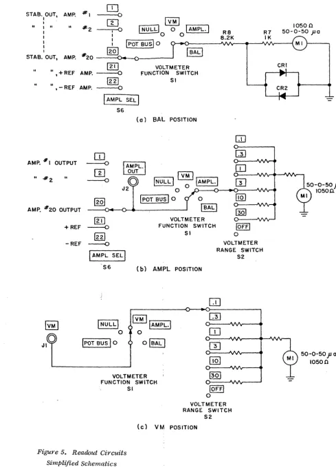
The BALposition of the Voltmeter Function Switch (Sl) is used when balancing the
dc amplifiers. The AMPL SEL switch (S6) is used to select the stabilizer output
of the amplifier to be balanced, (Figure Sa). The balance potentiometer of the
amplifier is rotated until the meter reads zero. Positions 1 to 20 of the AMPL
SEL switch are connected to the stabilizers of the 20 operational amplifiers;
positions 21 and 22 are connected to the stabLlizers of the plus and minus reference
amplifiers respectively. The diodes in parallel with the meter protect the meter
movement.
14
STAB. OUT, AMP. #1
I ,
I
II I II
..
#2 I I I I I
STAB. OUT, AMP. #20
[JJ
- - - 0
[TI
~---:-... 0
I
NULg 0I
AMPL.II
0 0 : IpOT BUS] 01201
@JJ
II
,+REF AMP. - - - 0 FUNCTION VOLTMETER SWITCH SI
II
, -REF AMP.
1221 - - - 0
AMP. # I OUTPUT
II
-#2 II
AMP. #20 OUTPUT
+ REF
I
AMPL SEL] S6(a) SAL POSITION
[IJ
- - 0
I
AMPL.\
rn
OUT~
- - 00
INULLI
0 IAMPL.IJ2 0
[Q]
IpOT BUS 10 0 IBALI[ill VOLTMETER
- - 0 FUNCTION SWITCH SI R8 8.2K
OJ
~ 10FFI 0[g]
-REF - - . ( ) VOLTMETER
I
AMPL SELlRANGE SWITCH
S6 ( b) AMPL POSITION
INULLI
o
IpOT BUS
I
0VOLTMETER FUNCTION SWITCH
SI 10FFI
o
VOLTMETER RANGE SWITCH
[image:23.631.69.558.78.757.2]S2 (e) VM POSITION
Figure 5. Readout Circuits Simplified Schematics
S2
10500 50-0-50 jJa
CRI
CR2
-50 -0--50 jJ a
10FFI
1+101
82J
IAMPLI
o +IOV 0 0 -IOV
VOLTMETER FUNCTION SWITCH
SI
o
I
BALI
R7 IK
(d) NULL POSITION
R9 2.2K
r---
II
r:::::1 II +IOVI
~I
I
~
05QJ
VOLTMETERII 6_
+IOV O----IOV FUNCTION SWITCHI
rSI
RIO 2K
S3
R9 2.2K
I
IVM
I
I
I
NULLI
0I
AMPLI
~T BUSI
0 0I
BALI
o
S3
INULLI POT RIO
READOUT SWITCH
ATTEN.
12.265
'---+---=----=---e-... TO OTHER
ATTENUATORS
CONTROL PANEL 20.734
i
L ________________________
~The ;21PL position of the Voltmeter Function switch establishes the circuit shown in Figure Sb where the output of the selected amplifier provides the input to the volt=etero The Voltmeter Range switch is used to select a convenient full-scale
range for the voltmeter. Note that the wiper of the AMPL SEL switch is connected to the AMPL OUT jack so that amplifier outputs can be monitored with external equipment-.
The VM position of the Voltmeter Function switch connects the VM jack to the Voltmeter Range switch (Figure Sc). Voltages patched into the VM jack are read on the voltmeter.
The NULL position of Sl provides a means of accurately measuring unknown voltages with respect.to the computer reference voltage. The circuit arrangement is shown in Figure Sd. The voltage to be measured is patched to the VM jack and connected to one side of the meter. The wiper of the NULL POT is connected to the other side of the meter. The Reference Selector switch S3 is switched to the position that supplies reference voltage with the same polarity as the voltage to be measured. .The NULL POT is varied until the meter reads zero. The position of
the turns-counting dial on the NULL POT indicates the magnitude of the unknown voltage; the position of S3 indicates the polarity of the unknown voltage. This null comparison method of voltage measurement is accurate to within ±p.l% of full
scale.
An
important feature of the method is that no current is drawn from the source being measured once a balance is attained. Thus the resistance of the source has no effect in the measurement. A large source resistance, however, will decrease the- sensitivity of the meter to unbalanced conditions.The POT BUS position of Sl is used when setting attenuators (Figure Se). The readout circuit is connected to measure the voltage on the pot bus by the null comparison method. When the pushbutton switch associated with an attenuator is depressed, +10 volts is connected to the top of the attenuator, and the wiper is connected to the pot bus. The Reference Selector switch, S3 must be in the +10 position. The NULL POT is set to the desired attenuator coefficient. The atten-uator is adjusted until the meter reads zero. The attenuator is then set to the
same coefficient as the NULL POT.
b. Manual Mode Control
The Mode Control switch (8S) on the Control Panel provides a means of starting and stopping computer solutions and of establishing initial conditions. The switch controls the operation of a circuit which actuates the reset and operate
relays of the integrators. The switch positions are RESET, HOLD, and OPER (operate). All computing components except the integrators are operational in all three modes. The integrators are controlled as follows:
RESET
HOLD
OPER
4. ATTENUATORS
In the reset mode, the output voltages of the integrators are set to the values required by
initial conditions of the problem. All other
inputs to the integrator are disconnected.
In the hold mode, the inputs to the integrators are removed; integration ceases and all vari-ables are held at the present values.
In the operate mode, the integrators accept inputs and integration with respect to time takes place.
One of the simplest and most useful operations performed on an analog computer is accomplished by using a potentiometer to multiply a voltage by a positive constant
that is less than one. This corresponds to attenuation of the voltage, therefore
potentiometers are often called attenuators. Both terms are used interchangeably
here. Four types of attenuator groups are available for use in the TR-20, All
groups use ten-turn, 5000 ohm potentiometers. The groups are listed below.
GROUP NO. OF POTS TYPE OF POT DIAL REMARKS
42.183 2 Carbon Uncalibrated Does not have Readout
Switches
42.187 2 Carbon Un c-a 1 i brated Has Readout Switches
42.188 2 Wirewound Calibrated Has Readout Switches
2.1,28 Has Readout Switches
(42.185
&
12.265) 4 Wirewound Calibrated Pots located in
Con-trol Panel area
The Type 42.183, Type 42.187, and Type 42.188 Groups have similar patching
termina-tions. The top potentiometer is terminated on the left side of the patching module
and the lower end of this potentiometer is grounded. The lower potentiometer is
terminated on the right side of the patching module and both ends of the
potentio-meter are available for patching. The Type 2.128 Group consists of a patching
module (Type 12.265) that mounts in the non-linear row of computing components,
and Quad Coefficient Assembly, Type 42.185 that mounts in the control panel area.
The lower end of each potentiometer is grounded. The potentiometers are
termina-ted in order, top to bottom, on the patchirg module.
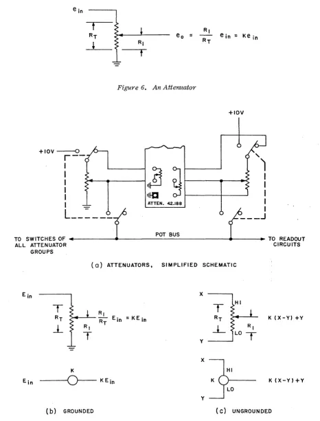
When an input voltage E. is applied to an attenuator as shown in Figure 6, the
In
R
output voltage Eo is K times E
in, where K
=
l/~.
If the attenuator is unloaded,the mechanical ratio of Rl :R
T is the same as the electrical ratio E o :E. In and the
attenuator could be set to the exact ratio by means of the vernier dial attached to
the wiper shaft. Normally, however, the attenuator is loaded and the two ratios
are not equal. The most common use of the attenuator is to feed an amplifier; thus
the wiper is loaded by the amplifier input resistor. In order to account for loading,
i t is more convenient to set the attenuator under loaded conditions by monitoring the wiper voltage and adjusting the wiper until the desired output is obtained.
Figure 7a shows the circuit used in the TR-20 to permit setting grounded attenuators
under load. A pushbutton switch is located next to each attenuator; depressing the
switch connects the wiper to the pot bus, removes the voltage applied at the patch
panel, and applies +10 volts to the top of the attenuator. The wiper voltage, on
the pot bus, can be measured by the null-comparison method by using the NULL POT
on the control panel.
The ungrounded attenuators are connected in the circuit configuration shown in
Figure 7b. Depressing the pushbutton switch applies +10 volts to the top of the
potentiometer and connects the loaded wiper to the pot bus for measuring purposes. Note that the lower end of the attenuator is not grounded and voltages may be patched
to both ends of the attenuator. The patching block has a ground termination near
the low end of the ungrounded potentiometer to make i t convenient to ground the low end if so desired.
The Type 42.183 Attenuator Group does not include the pushbutton switches. The wiper
of each attenuator is brought out to a termination next to the attenuator to
facil-itate readout under loaded conditions. Figure 7 contains schematics and symbols for
two potentiometer types. The address or number qf the potentiometer (i.e., 1 or 2)
is placed within the circle; the coefficient setting (K) is written near the symbol.
The high and/or low end of ungrounded potentiometers is also indicated.
5. THE OPERATIONAL AMPLIFIER
a. General Considerations
When a high-gain dc amplifier is used in conjunction with input and feedback networks to perform mathematical operations, the resulting system is generally referred to as
an operational amplifier. The operational amplifier is the basic and most versatile
unit in the analog computer. It can be used for inversion, summation, multiplication
by a constant, integration, and used in conjunction with special networks for squar-ing,extracting square root, generating logarithmic functions, etc.
e in = Ke in
Figure 6. An Atterl1lator
+IOV
+IOV---O
r--
,
I
I
I
::~ ~
t - - - + - - - J!
I I
L--=----i
ATTEN.42.188L---
J
POT BUS
TO SWITCHES OF ~.~---~---~----~~~ TO READOUT
ALL ATTENUATOR CIRCUITS
GROUPS
(0) ATTENUATORS, SIMPLIFIED SCHEMATIC
x
RI
~-'-- RT Ein = KE in
R,
T
T
HIRT K (X-Y) +Y
L
RILO
T
YX K
Ein
- - 0 -
KEin K(X-Y)+YY
(b) GROUNDED (C) UNGROUNDED
Recall that the amplifier is designed to have three essential characteristics (see Figure 8):
(1) The amplifier output (eo) is related to the summing junction voltage (lb) by the gain of the amplifier: eo
=
-Aeb
(2)
(3) order of 3 X
The input stage of -the amplifier draws negligible current: ib~ 0
Thg open loop gain of the amplifier is extremely high: A»l (on the
la' at dc).
Therefore, the amplifier output voltage is related to the input voltage by the equation:
e = - - e
( Zf )
o Zinl in CEQ. 2-1)
Equation 2-1 '::'::lustrates one of the most important characteristics of the oper-ational amp1i=~:2r: the input-output relationship of the operational amplifier is solely depenc~~= on the ratio of the feedback to the input impedance.
Using Equatio~ 2-1 as the basis of discussion, the following sub-paragraphs describe the -various u:s.:2:.:S of the opera tiona 1 amplifier.
When the same ~(C".2.1ue resis tor is used for both the feedb9ck
the amplifier ":::'utput voltage has the same amplitude as the opposite in p~~rity. In the TR-20 the value of R
f and R. ln
norma 11y 100, C-:\:1 ohms (lOOK), there fore:
e
o e. ln
lOOK
lOOK e in e. ln
and the input impedance, input voltage but is
used for the inverter is
Thus a +10 vo=-::..- input results in a -10 volt output, and the amplifier is said to have a gain
0=
~inus one. The accuracy of the output to input ratio depends solely on the accurac of the ratio Rf/R . .ln
.£. Mu1tip_---=--cation by a Constant A change in th':::::~
examp 1e, wi th
ratio of the resistors results in multiplication by a constant.
~ equal to lOOK and R. equal to 10K, the amplifier output is:
ln
e o
lOOK
10K e. ln 10e. ln
For
Figuye 8. Operational Amplifier, Simplified Block Diagram
An input of plus one volt results in an output of minus ten volts. This operational amplifier has a gain of ten. The multiplying constant can be made smaller than one by using a 10K feedback resistor with a lOOK input resistor.
e o
10K
lOOK e. ~n -0. le . ~n
An input of minus ten volts produces an output of plus one volt. ~. Surrnnation
When multiple input resistors are used with a feedback resistor R
f, the basic re-lationship is extended to:
The circuit can be used to algebraically sum an indefinite number of inputs; further-more, each input may be multiplied by an arbitrary constant.
~. Integration with Respect to Time
When the feedback element Zf is a capacitor rather than a resistor, the operational amplifier becomes an integrator. If Zf is a capacitor having an operational imped-ance l/pC and Z. is a resistor, the Easic operational amplifier relationship,
~n
Equation 2-1, becomes:
E.
~n
e
-o pRC
1 t
- RC
So
e. ~n dtAn indefinite number of inputs may be applied to produce the time-integral of the sum of the input voltages.
f. Other Mathematical Operations
As previously indicated, the operational amplifier has uses other than those de-scribed above. Complicated transfer functions can be simulated by using series and parallel RC networks for the feedback and input impedance. The circuit per-formance is still governed by the basic relationship of Equation 2-1. For the general case where three-terminal networks are used, the short-circuit transfer
impedance of Zf and Z. must be used. The input and feedback elements need not be linear; therefore, al~gst any non-linear characteristics can be approximated. The amplifier can also be used in conjunction with diodes and resistors to simulate the non-linear operations of limiting, dead-zone generation, X2, Log X, etc.
£.
Patching the ~3plifier as a Summer/InverterFive precision input/£eedback resistors are terminated at the front of each ampli-fier section of the pEtch block. Three of these resistors have a value of lOOK each, and are designated 1 on the patch block. The two remaining resistors, with a value of 10K each, are connected to terminals designated 10. The other end of each resistor is connected to a common bus, and terminated at a point designated SJ
(summing junction) on the patch block. The input of the amplifier is terminated at a point designated B (base), and the output of the amplifier is connectd to five 0 terminals in the red area of the patch block.
To patch an amplifier as a summer or inverter, insert a double (four-prong) bottle plug as shown in the upper amplifier of Figure 3a. A voltage applied to one of the 1 input terminals is multiplied by -1, and the amplifier is referred to as an in-verter (Figure 3b). If two inputs (for example x and y) are connected to the 1
inputs as shown in Figure 3c, the output of the amplifier is equal to -(x
+
y), and the amplifier is acting as a summer.The lower amplifier of Figure 3a is patched with two prong bottle plugs to provide one gain-of-one input and three gain-of-one-tenth inputs~ as shown in Figure 3d.
h. Patching the Amplifier as an Integrator
The amplifier becomes an integrator by providing the proper patching connections to an integrator network. Two types of integrator networks are available for the TR-20. Each network contains the passive elements and control circuits necessary
to form two integrators. The Model 12.1116 is supplied with computers that are not equipped for repetitive operation. The Model 12.1115 is supplied as a part of the repetitive operation expansion group (see Section 11 of this chapter). Both net-works are similar, and are ~escribed here.
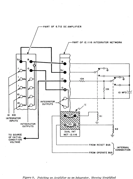
(1) Integrator Network 12.1116. Figure 9 is a diagram which illustrates the patching required to convert an amplifier into an integrator. The patching is straight-forward, with the S4, 0, and B terminals of the amplifier connected to the SJ, 0, and B terminals respectively of an integrator network. Two additional
patching connections are required on the 12.1116 Integrator Network, indicated by the heavy lines in the lower cross-hatched area of the integrator patch block
(Figure 9). These connections may be easily made by inserting two-prong bottle plugs in this area.
The diagram at the right side of Figure 9 shows the essential components of one half of a dual integrator network. The relays (Kl and K2) are common to both
sections of the network, although only one set of contacts is shown for each. Both relays are shown de-energized, as they exist in the hold mode. In this mode, the inputs at the SJ terminal are connected to ground by the contacts of Kl. The initial condition voltage is also connected to ground (through a 10K resistor) by the con-tacts of K2. The capacitor remains connected as the feedback element of the ampli-fier, between the Band
°
terminals. This allows the capacitor to retain any volt-age which may have been applied during the operate or reset modes, and the output of the integrator remains constant.XI XlO INTEGRATOR
INPUTS
INTEGRATOR OUTPUTS
TO SOURCE OF INITIAL CONDITION VOLTAGE
PART OF 6.712 DC AMPLIFIER
PART OF 12.1116 INTEGRATOR NETWORK
INTEGRATOR OUTPUTS
B
SJ
IC
DUAL INT NET 12.1116
10K
KI 10K
I
I
I I
-I
I
I
10 MFD
K2
INTERNAL FROM RESET BUS
J
[image:33.612.69.537.73.699.2]CONNECTION ' - - - FROM OPERATE BUS
Figure 9. Patching an Amplifier as an Integrator, Showing Simplified Schematic of an Integrator Network
When the computer is placed in the reset mode, relay voltage is present on the reset bus. If the indicated patching connection in the RS area is made, K2 is energized, and its contact moves to the alternate position shown. This allows a voltage at the IC terminal to be coupled through a 10K input resistor to the base of the ampli-fier. The feedback capacitor is now shunted by a 10K resistor. This allows the amplifier to perform as a unity-gain inverter (for the initial condition voltage) with a time lag of approximately 0.5 seconds. For this reason, the computer should
always be left in the reset mode for at least one-half second before switching to the hold or operate modes, to assure that the correct initial condition potentials are established.
When the computer is switched to the operate mode, K2 de-energizes and Kl energizes. This applies the input potentials at the SJ terminal of the network to the base of
the amplifier. Since K2 is de-energized, the capacitor provides the only feedback path for the amplifier, and integration with respect to time takes place. .
The patching connections in the cross-hatched area have been indicated for stand-ard operation. For special situations, these connections may be different. For example, if the RS connection is deleted, the integrator cannot be placed in the reset mode; remaining in hold when the other integrators in the computer are being reset. This allows the value reached during a solution to be used as an initial condition for the next solution. Patching and a brief description of these spe~ial
situations is provided in the appendix.
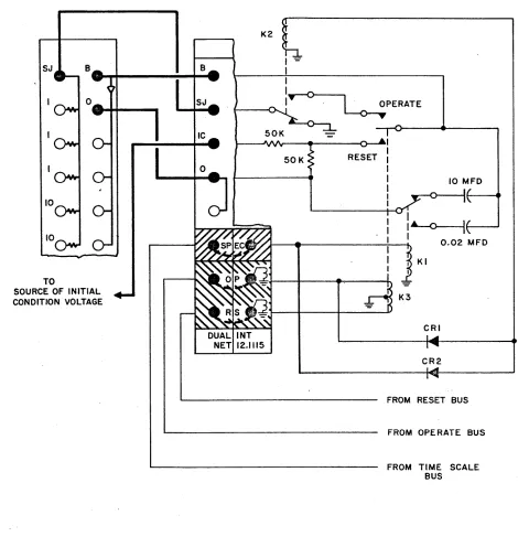
(2) Integrator Network 12.1115. This network differs from th~ network pre-viously described principally by providing two values of feedback capacitor. These values (10 mfd and 0.02 mfd) allow a 500 to 1 change in time scale. Figure 10
illustrates the patching connection and the circuit arrangement of the network. Note that the patching connections to the amplifier are identical to those for a 12.1116 Network. An additional patching connection is required on the integrator network in the cross-hatched area designated SPEC, if the integrator is to be used
in the standard rep-op mode.
The Operate and Reset relays (Kl and K2 of Figure 9) have been replaced by a single balanced-armature relay (K3 of Figure 10). This allows the integrator to be switched between operate and reset modes very rapidly, a necessary requirement for repetitive
operation. Relay Kl selects the correct value of feedback capacitance for normal or repetitive operation. If the connection in the SPEC area is delected, the inte-grator has a feedback capacitance of 10 mfd for either mode. T~is patching is de-scribed in the appendix.
Relay K2 grounds the SJ input during the reset and hold modes. The relay is ener-gized during the operate and rep-op modes, through CRl or CR2 respectively. When K2 is energized, the SJ input is connected to the operate contact of the Repetitive Operation relay (K3). Therefore, when a problem is being set up on a computer equipped with the 12.1115 Networks, the Mode Control switch must be placed in the RESET position and the COMPUTE TIME MILLISEC switch must be placed· in the OFF position.
SJ
10
TO
SOURCE OF INITIAL CONDITION VOLTAGE
B
SJ
DUAL INT NET 12.1115
50K RESET
10 MFO
l
A-o---if---...
J--~--_ _ _ _ +---+..I 0.02 MFDKI
K3
CRI
CR2
FROM RESET BUS
FROM OPERATE BUS
[image:35.612.72.542.172.678.2]FROM TIME SCALE BUS
Figure 10. Patching an Amplifier to a Rep-Op Integrator, Showing Simplified Schematic of Integrator Network
6. Q~~RTER-SQLARE MULTIPLIER
a. General Description
The quarter-square multiplier is used in conjunction with a dc amplifier to pro-duce a four quadrant product proportional to XY from inputs of +X, -X, +Y, and
-Yo In addition to multiplication, the TR-20 multiplier is capable of performing
the mathematical operations of division, squaring, and square root extraction.
The operation of the quarter-square multiplier is based on the identity:
which reduces multiplication to the operations of summation and squaring. The
squaring operations are performed by diode function generators (DFG's) that
con-tain biased diode networks. The diode function generators or squaring cards
gen-erate a segmented straight-line approximation to a square law curve. The complete
multiplier assembly contains four squaring cards that are connected so as to permit
multiplication of input signals of either plus or minus polarities. (Only two of
the squaring cards conduct at anyone time.) The outputs of the squaring cards
are summed in an external amplifier.
Operators who are interested in the circuit details of the quarter-square multi-plier are referred to the TR-20 Maintenance Manual.
b. Multiplication
The general configuration of the quarter-square multiplier is shown in Figure lla. The DFG's contain biased diode networks' that produce a current proportional to the square of the sum of the input voltages to the DFG when the sum of the input
volt-ages has the proper polarity. A positive DFG conducts only when the sum of its
inputs is positive.
The unit is patched as a multiplier in Figure llb. The squaring cards (DFG's)
form the input network of the amplifier; a 3550 ohm resistor (R65) is the
feed-back element. The input voltages are patched to the +X, -X, +Y, and -Y terminations.
The output voltage from the amplifier is -
~~.
The output is changed to +~~
byreversing the +X and -X inputs or the +Y and -Y inputs. All four input voltages
must be patched in. The squaring cards have a variable input impedance, therefore
the input voltages should not be obtained from potentiometers. The output
ampli-fier can be used to sum additional inputs; the gain for an additional 10K ohm in-put resistor is 0.355 since the amplifier has a 3550 ohm feedback resistor.
A programming symbol for the multiplier is shown in Figure llc.
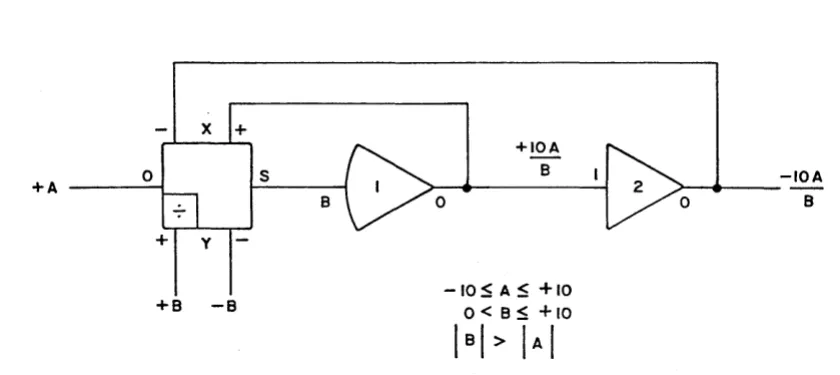
c. Division
Division of a variable voltage A by a variable voltage B is accomplished by placing
+Xo
DFG
>-+IN
-X
J
~ DFGr--- +IN
So
- - 1 DFG
+xo
+x-X~
-x8~0
So
V
+YO -IN +Y
O
+yD F G >
-Y
J
-IN R65 .~ 3550>
-Y~
-y°0
°0
MULT MULT
7.045 7.045
o. SIMPLIFIED DIAGRAM OF UNIT :b. MULTIPLIER PATCHING
0
+X +X
S 8. 0 -xv
-X -X 10
-y +y
-y
c. SYMBOL
Figurf! 11. Quarter-Square Multiplier Patching
-xv
10
the multiplier in the feedback loop of a high-gain amplifier as shown in Figure 12. Assume that the output voltage of amplifier 1 is C; then at the summing junction of amplifier 1, the null relationship
CB
+
A10
o
is satisfied by automatic changes in the value of C. Therefore:
C - -
lOA
B
Note that although the voltage A can have both positive and negative values, the voltage B must always be positive. If B is always negative, then the use of -B
in its place (by interchanging the inputs to +Y and -Y) will produce
C
+
lOAB
at the output of amplifier 1.
The following restrictions must be placed on the division circuit:
(~) The absolute value of the divisor B must be greater than or equal to the absolute value of the dividend A to avoid overloads in the output amplifiers.
(~) The divisor B must not change sign. It must not go to zero, for this implies an indeterminate or infinite quotient. The circuit requires that the high-gain amplifier (amplifier 1) be surrounded by negative feedback, and this can only be arranged for one or the other polarity of the voltage B.
Circuits using the quarter-square multiplier are summarized in the appendix.
7.
x
2 DIODE FUNCTION GENERATOR a. General DescriptionThe X2 Diode Function Generator is used in conjunction with a dc amplifier to pro-duce an output voltage that is proportional to the square or square root of the inpu t vo 1 tage.
The X2 DFG contains two independent sections that generate quadratic curves. One accepts positive input voltages; one accepts negative input voltages. Biased diode networks similar to those in the quarter-square multiplier are used to approximate