Charging dynamics of a floating gate transistor with site-controlled quantum dots
P. Maier, F. Hartmann, M. Emmerling, C. Schneider, S. Höfling, M. Kamp, and L. Worschech
Citation: Applied Physics Letters 105, 053502 (2014); doi: 10.1063/1.4892355
View online: http://dx.doi.org/10.1063/1.4892355
View Table of Contents: http://scitation.aip.org/content/aip/journal/apl/105/5?ver=pdfcov
Published by the AIP Publishing
Articles you may be interested in
Cavity-enhanced single photon emission from site-controlled In(Ga)As quantum dots fabricated using nanoimprint lithography
Appl. Phys. Lett. 104, 213104 (2014); 10.1063/1.4879845
Charge storage properties of InP quantum dots in GaAs metal-oxide-semiconductor based nonvolatile flash memory devices
Appl. Phys. Lett. 101, 212108 (2012); 10.1063/1.4767522
Size evolution of site-controlled InAs quantum dots grown by molecular beam epitaxy on prepatterned GaAs substrates
J. Vac. Sci. Technol. B 24, 1523 (2006); 10.1116/1.2190674
Trench-type InGaAs quantum-wire field effect transistor with negative differential conductance fabricated by hydrogen-assisted molecular beam epitaxy
J. Vac. Sci. Technol. B 20, 1192 (2002); 10.1116/1.1456519
Patterned growth on GaAs (311)A substrates: Dependence on mesa misalignment and sidewall slope and its application to coupled wire-dot arrays
Charging dynamics of a floating gate transistor with site-controlled quantum
dots
P. Maier,a)F. Hartmann, M. Emmerling, C. Schneider, S. Hofling,€ b)M. Kamp, and L. Worschech
Technische Physik, Physikalisches Institut, Wilhelm Conrad Rontgen Research Center for Complex Material€
Systems, Universitat W€ urzburg, Am Hubland, D-97074 W€ €urzburg, Germany
(Received 16 May 2014; accepted 20 July 2014; published online 4 August 2014)
A quantum dot memory based on a GaAs/AlGaAs quantum wire with site-controlled InAs quantum dots was realized by means of molecular beam epitaxy and etching techniques. By sampling of dif-ferent gate voltage sweeps for the determination of charging and discharging thresholds, it was found that discharging takes place at short time scales ofls, whereas several seconds of waiting times within a distinct negative gate voltage range were needed to charge the quantum dots. Such quantum dot structures have thus the potential to implement logic functions comprising charge and time de-pendent ingredients such as counting of signals or learning rules.VC 2014 AIP Publishing LLC.
[http://dx.doi.org/10.1063/1.4892355]
Quantum dots (QDs) located in close vicinity of transis-tor channels can induce significant threshold voltage shifts, which depend on the number of QD localized charges, the capacitive coupling, and the electrochemical properties.1–3 The floating gate function of QDs has been demonstrated in different material systems such as lithography defined1and self-assembled QDs4–7and down to the quantum limit of one electron.1,8,9Since self-assembled QDs are randomly distrib-uted, charges on several QDs contribute to the threshold volt-age shift. Thus, ensembles of QDs are typically not practical for the study of single electron properties. Therefore, an accurate control of the number of QDs and their relative dis-tances to the gates is necessary.
Here, we report on the realization of a QD flash memory based on a modulation doped GaAs/AlGaAs heterostructure with site-controlled InAs QDs located in the center of a quan-tum wire. The central QD becomes charged at negative gate voltages. By sampling different gate voltage sweeps with var-iations in the minimum gate voltage and waiting time, the charge occupation number of the QDs can be controlled in a wide range. A maximal hysteresis width of 6.2 V is found. Time resolved measurements show QD charging times of several seconds.
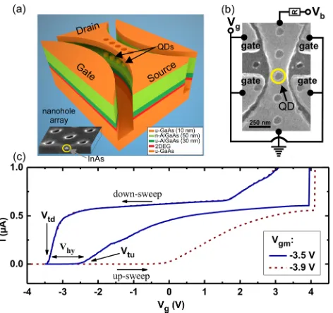
A sketch of the device is shown in Fig. 1(a). The QD floating gate transistor was grown by molecular beam epitaxy in two steps. Starting with an undoped GaAs substrate, 30 nm of undoped Al0.2Ga0.8As followed by 50 nm of n-doped Al0.2Ga0.8As were grown in the first growth process. On top of the heterostructure, a 10 nm thick and undoped GaAs layer was deposited. Afterwards, nanohole arrays were processed by electron beam lithography and soft dry chemical etching with a period of 300 nm and a hole diameter of around 100 nm. The depth of the nanoholes is around 50 nm. This results in a 40 nm thick Al0.2Ga0.8As layer between the
nanohole and the two-dimensional electron gas (2DEG). The diameter of 100 nm was selected because of optimal fabrica-tion parameters, e.g., e-beam lithography resolufabrica-tion and InAs quantum dot formation. In the second growth process, InAs was deposited on the structure, which leads to InAs QDs in the holes.10Finally, the InAs QDs were capped with GaAs. A detailed description of the growth technique is given in Refs. 2and11. The inset of Fig.1(a)shows an electron microscope image conducted from a tilted angle of the structure right af-ter the InAs growth. The sample was etched in such a way that the front cuts through a nanohole. The bright spot inside the nanohole corresponds to InAs. After the growth proce-dure, a Hallbar was realized by optical lithography, wet chemical etching, and alloying of Ni/AuGe/Ni/Au contacts. Finally, the QD floating gate transistor was defined by elec-tron beam lithography in combination with a soft dry chemi-cal etching technique. Dry chemichemi-cal etching was performed to isolate the gate from the channel area via trenches with a depth of 150 nm.
An electron microscope image of the device together with the circuit diagram is shown in Fig.1(b). The device consists of a transport channel, four laterally defined side gates and site-controlled QDs above the channel. The gate voltage Vg and the bias voltageVbwere applied to the side gates and the top contact, respectively, with the bottom contact serving as common ground. The current was measured as voltage drop across a series resistor withR¼10 kX. All measurements were conducted at 4.2 K in the dark. The channel width at the small-est constriction is aroundw210 nm. The position of the cen-tral site-controlled QD is highlighted by a yellow circle. In Fig.1(c), two current-gate voltage tracesI(Vg) are shown. The gate voltage was swept from a minimum gate voltage Vg¼Vgm¼ 3.5 (solid) or3.9 V (dashed) toVg¼4.5 V (up-sweep direction) and back (down-(up-sweep direction) for a con-stant bias voltage Vb¼0.1 V. The arrows indicate the gate voltage sweep cycle directions and the corresponding threshold voltagesVtufor the up- andVtdfor the down-sweep. Starting with a pinched-off channel atVg¼Vgm¼ 3.5 V, the channel opens when the gate voltage passes the threshold voltageVtu.
a)
Author to whom correspondence should be addressed. Electronic mail: [email protected].
b)Present address: SUPA, School of Physics and Astronomy, University of
St. Andrews, North Haugh, KY16 9SS St. Andrews, United Kingdom.
0003-6951/2014/105(5)/053502/4/$30.00 105, 053502-1 VC2014 AIP Publishing LLC
The current increases monotonically up to aboutVg4 V, at which an almost instantaneous jump of the current occurs. For the down-sweep, the current decreases slightly until it drops to zero when the gate voltage passesVtd. A hysteresis between Vtd and Vtu is evident with a hysteresis width of Vhy¼Vtu Vtd¼0.9 V. AtVg¼ 2.86 V, the current isIh¼0.5lA in the down-sweep andIl¼500 pA in the up-sweep. Thus, the on-off current ratioIh/Ilis 1000. One can see when the minimum gate voltage is reduced toVgm¼ 3.9 V, that the down-sweep
trace remains almost unaltered with a similar valueVtd, while the up-sweep trace differs significantly.Vtushifts to higher gate voltages withVtu(Vgm¼ 3.9 V)¼3.3 V>Vtu(Vgm¼ 3.5 V).
Experimentally determined dependencies of Vtd and Vtu onVgm are shown in Fig.2(a). The measurements were con-ducted in the following way. Vgm was first set to a constant value, e.g., 3.46 V. Then, the gate voltage was swept at a constant sweep rate of DVg/Dt¼0.2 V/s from Vgm to Vg¼4.5 V and back toVgm.VtuandVtdwere determined. Such measurements were repeated several times. Each data point in Fig.2(a)represents the average value of forty closed gate volt-age cycles. This procedure was performed forVgmfrom3.46 to 4.50 V. As depicted in Fig.2(a),Vtuincreases from2.8 to þ2.8 V when Vgm is lowered but saturates below Vgm 4.2 V. In contrast Vtd remains constant and is inde-pendent ofVgm.
The shift of the threshold voltageDVtuto higher values for a reduction of Vgm is explained by the charging of the central QD with DVtu¼DQ/Ceff.
1,3,9
The capacitance Ceff describes the Coulomb coupling between the gate, the QD, and the channel for a given amount of QD localized charge Q¼nq. Here,qis the elementary charge andnis the number of electrons. Thus, theVtu(Vgm) curve shows that a reduction of Vgm corresponds to an increased amount of electrons on the QD withQ/Vgm. Interestingly, the charging process of the QD occurs when the quantum wire is depleted for gate voltages smaller than Vtd. We emphasize that the observed charging process at negative gate voltages is in contrast to the typical floating gate function of transistors with a top gate structure, in which charging is observed for positive gate voltages.1,12,13 The negative charging voltages are attributed to the side-gate geometry. Here, the in-plane gates result in a more efficient shift of the electrostatic channel potential compared to the potential change of the floating-gate. Thus, at negative gate voltages, the electrostatic chan-nel potential exceeds the one of the quantum dot so that the QD becomes charged.
SinceVtdis independent ofVgm, the charge on the cen-tered QD remains constant during the down-sweep. The in-stantaneous jump of the current at the gate voltageVg4 V (see Fig.1(c)) thus corresponds to a pronounced discharging of the QD. Time-resolved measurements show that the dis-charging process occurs in thels range.
Fig.2(b) displays the width of the hysteresisVhy¼Vtu Vtd versus the minimum gate voltage Vgm as obtained from the data depicted in Fig.2(a). SinceVtdis independent of Vgm, Vhy follows the threshold voltage Vtu of the up-sweep. The maximum hysteresis width isVth6.2 V forVgm smaller than 4.2 V and a maximal QD charge occupation Qmaxis reached. ForVgm¼ 3.46 V, the hysteresis still has a value ofVhy0.6 V and the QD is partially charged even for VgmVtd. In contrast to the discharging, which results in the steep current increase, the charging of the QD occurs for a pinched-off channel. Thus, the charging time cannot be extracted directly from theI-Vgcharacteristic.
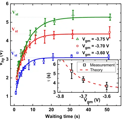
Fig.3depicts the waiting time dependence of Vhy for Vgm¼ 3.60,3.70, and3.75 V. The waiting time meas-urements were conducted in the following way. At t¼0 s, Vgm was set and kept constant for a given waiting time. Then, the gate voltage was swept from Vgmto Vg¼4.5 V FIG. 2. (a) Threshold voltagesVtuandVtdversus minimum gate voltageVgm.
Vtdis independent of Vgm. Vtu shifts from 2.8 toþ2.8 V whenVgm is
reduced from 3.46 to 4.50 V and saturates below Vgm¼ 4.2 V. (b)
Hysteresis widthVhyversus minimum gate voltageVgm.Vhyreaches a
maxi-mum ofVhy¼6.2 V belowVgm¼ 4.2 V with a maximum charge occupation
Qmaxon the QD. ForVgm¼ 3.46 V, the width of the hysteresis is still 0.6 V.
FIG. 1. (a) Scheme of the QD floating gate transistor. It is composed of a 2DEG transport channel, site-controlled InAs QDs, and laterally defined side gates. Inset: An electron microscope image taken from a tilted angle shows a cross section through a nanohole. The bright spot corresponds to InAs. (b) Electron microscope image together with electrical setup of the de-vice. The gate voltageVgwas applied to the four side gates. The bias voltage Vbwas applied to the top contact and the bottom contact was used as
com-mon ground. The QD located in the smallest constriction of the channel is highlighted by a yellow circle. (c) Current-gate voltage traces I(Vg) for Vgm¼ 3.5 (solid) and3.9 V (dashed) up toVg¼4.5 V. The arrows
indi-cate the up- and down-sweep directions with corresponding threshold vol-tagesVtuandVtdas well as the hysteresis widthVhy.
[image:3.612.58.294.52.274.2] [image:3.612.58.292.540.705.2](and back) at a constant sweep rate withDVg/Dt¼0.2 V/s. For each sweep cycle,Vtd,Vtu, andVhy were obtained and each data point in Fig.3corresponds to the average of five sweep cycles. When the waiting time is varied from 0 to 50 s for Vgm¼ 3.60 V, Vhy increases from 1.19 V until it saturates atVhy(t¼50 s)¼Vst¼3.10 V. For a reduction of Vgm, theVhy-waiting time curves behave qualitatively simi-lar but Vst increases to 4.37 (Vgm¼ 3.70 V) and 5.27 V (Vgm¼ 3.75 V).
We interpret the time evolution of Vhy in the following way. By settingVgmatt¼0 s, the electrochemical potentials of the QDlqand the source contactls differ withls>lq. The electrochemical potentials then start to align by charging of the QD via electron tunneling from the source contact untills¼lq. Fig.3thus resembles the time resolved charg-ing of a capacitor and the time evolution ofVhyfor eachVgm can be described by15
Vhy¼ðVstV0Þ 1exp t
s
þV0; (1)
wheresis the charging orRCtime constant given by the ca-pacitance C and resistance R. Vst is the saturation threshold voltage andV0considers dynamic effects of charging. The fit functions of the data from Fig.3with Eq.(1)lead to charging times of (5.360.8), (4.460.3), and (3.660.4) s for Vgm¼ 3.75,3.70, and3.60 V, respectively. Remarkably, sis in the order of a few seconds.sversusVgmis shown in the inset of Fig.3. One can estimate the tunneling resistanceRby s¼RC. The capacitance C of the QD is approximated by a planar disk with diameterd¼100 nm. With the dielectric con-stant of AlGaAser¼12.3e0(e0is the vacuum permittivity) we obtainC¼4erd¼43 aF.
16
The corresponding resistancesR are 1.2, 1.0, and 0.81017X forVgm¼ 3.75, 3.70, and 3.60 V, respectively. According to our observations an increase of the QD diameter would lead to larger capacitances, which in turn increases the charging times. We associated the
observed charging times sin the order of seconds with huge tunneling resistances. For clarity, Fig.4shows schemes of the device from the top (a) and conduction band profiles (b).
The top view image in Fig. 4(a) depicts the depletion region for two minimum gate voltagesVgm,1andVgm,2with Vgm,1>Vgm,2. The depletion lengthdlfrom the center of the QD to the contacts of the wire increases from dl,1 to dl,2 when the gate voltage is reduced from Vgm,1 to Vgm,2. We assume that the voltage dependent barrier width can be described by dl¼aðVgmVtdÞforVgm<Vtdanda<0. We further assume that the charging can be explained by tunnel-ing through a stunnel-ingle barrier for which the tunneltunnel-ing resist-anceRis proportional to expð2dpffiffiffiffiffiffiffiffiffiffiffiffiffiffiffiffiffi2mDE=hÞ,14,17whered
is the barrier thickness which equals
ffiffiffiffiffiffiffiffiffiffiffiffiffiffiffiffiffiffiffiffiffiffiffiffiffiffiffi d2
l þ ð40nmÞ
2 q
, m*is
the effective mass, andhis the reduced Planck constant.DE is the energetic difference between the top of the barrier and the electron energy. Thus, withs¼RC, the charging time is proportional to expðbðVgmVtdÞÞ. b accounts for the
con-stantsa, m*,h, andDE. This exponential dependence ofson the gate voltage is shown in the inset of Fig.3.
In Fig.4(b), schemes of the conduction band along the growth direction are shown for the source region and the channel below the central QD. The QD becomes charged with electrons from the source contact up to the electrochem-ical potential ls. The electrochemical potential of the chan-nel remains constant and thus no free electron states exist directly below the QD as the conduction band minimum is above ls. Thus, increasing the gate voltage results in free electron states in the channel and the QD becomes dis-charged atVg4 V. At this gate voltage, electrons can over-come the AlGaAs/GaAs barrier at the interface which reduces the tunneling barrier to about 20 nm, which leads to a significantly faster discharging process compared to the charging process. This is reflected in the steep current increase in Fig.1(c).
[image:4.612.74.280.52.252.2]To summarize, we have fabricated and measured a QD floating gate transistor based on a modulation doped GaAs/ AlGaAs heterostructure with site-controlled InAs QDs. The central QD becomes charged at negative and discharged at positive gate voltages. We observed charging times in the FIG. 4. Schemes of the charging time-gate voltage relation forVgm,1>Vgm,2.
(a) The central QD is charged when the 2DEG below the QD is depleted by the applied gate voltage. The electron tunneling distance from the source to the QD is enhanced withdl,2>dl,1whenVgm,1>Vgm,2. The QD is charged
[image:4.612.333.540.53.180.2]over a distance of several 100 nm from the source contact of the device. The discharging of the QD to the channel is blocked, because the electrostatic potential of the channel below the QD (b) is above the electrochemical poten-tial of the QD. This results in a blockade for discharging the QD.
FIG. 3. Waiting time dependence of Vhy for Vgm¼ 3.60, 3.70, and
3.75 V. For constantVgmand increasing waiting time,Vhygrowths until
the saturation voltageVstis reached. For waiting times of 50 s,Vstincreases
when the minimum gate voltage is reduced. The solid lines are exponential fit functions according to Eq.(1). Inset: The charging timesdecays expo-nentially with increasingVgm.
order of several seconds when the gate voltage is in a critical range between3.5 and 3.9 V. The presented single QD floating gate transistor may be used to realize low energy consuming memories or logic functions.
The authors gratefully acknowledge financial support from the European Union (FPVII (2007–2013) under Grant Agreement No. 318287 Landauer) as well as the state of Bavaria.
1
L. Guo, E. Leobandung, and S. Y. Chou,Science275, 649 (1997).
2
S. G€opfert, L. Worschech, S. Lingemann, C. Schneider, D. Press, S.
H€ofling, and A. Forchel,Appl. Phys. Lett.97, 222112 (2010).
3C. R. M€uller, L. Worschech, and A. Forchel,Phys. Rev. B 79, 205307
(2009).
4
A. Marent, T. Nowozin, M. Geller, and D. Bimberg, Semicond. Sci.
Technol.26, 014026 (2011).
5C. Balocco, A. M. Song, and M. Missous,Appl. Phys. Lett.85, 5911 (2004). 6
K. Koike, S. Sasa, M. Inoue, and M. Yano,J. Vac. Sci. Technol., B21,
710 (2003).
7T. Ohori, Y. Ohno, K. Maehashi, K. Inoue, Y. Hayashi, and K.
Matsumoto,Appl. Phys. Lett.98, 223101 (2011).
8
A. Nakajima, T. Futatsugi, K. Kosemura, T. Fukano, and N. Yokoyama,
Appl. Phys. Lett.70, 1742 (1997).
9L. Guo, E. Leobandung, L. Zhuang, and S. Y. Chou,J. Vac. Sci. Technol., B15, 2840 (1997).
10
C. Schneider, M. Strauß, T. S€unner, A. Huggenberger, D. Wiener, S.
Reitzenstein, M. Kamp, S. H€ofling, and A. Forchel,Appl. Phys. Lett.92, 183101 (2008).
11
C. Schneider, A. Huggenberger, T. S€unner, T. Heindel, M. Strauß, S.
G€opfert, P. Weinmann, S. Reitzenstein, L. Worschech, M. Kamp, S.
H€ofling, and A. Forchel,Nanotechnology20, 434012 (2009).
12P.-F. Wang, X. Lin, L. Liu, Q.-Q. Sun, P. Zhou, X.-Y. Liu, W. Liu, Y.
Gong, and D. W. Zhang,Science341, 640 (2013).
13
B. Marquardt, M. Geller, A. Lorke, D. Reuter, and A. D. Wieck, Appl.
Phys. Lett.95, 022113 (2009).
14R. Waser,Nanoelectronics and Information Technology, 3rd ed. (Wiley,
Weinheim, 2012), p. 626.
15
R. A. Serway, J. S. Faughn, C. Vuille, and C. A. Bennett, Enhanced
College Physics, 7th ed. (Thomson Brooks/Cole, Belmont, 2006), p. 605.
16J. D. Jackson,Classical Electrodynamics, 2nd ed. (John Wiley and Sons,
New York, 1975), p. 133.
17
J. G. Simmons,J. Appl. Phys.34, 1793 (1963).