Operational Amplifier
Preparation Work for the “Op-Amp Laboratories”
The next set of Labs are concerned with Operational Amplifiers. The characteristics of Op Amps as well as various applications including amplifiers, filters, comparators, oscillators, and wave form generators will be investigated and studied.
This material is intended as a review of Op Amps and as a guide in preparing for the Op Amps Labs. An outline of the steps to follow is
1. Obtain copies of the specification sheets for the 741, TL081 and TLE2037 operational amplifiers.
2. Quickly read the rest of this document. Pay attention to the questions.
3. Read chapter 2 in Sedra and Smith. Keep the questions in mind as you read. Jot down some notes as you go.
4. When you have finished the reading, try to answer the questions. Note that these questions are posed as a study guide only. It is not necessary to answer these questions in your Laboratory Notebook or in a “written assignment” form.
Real operational amplifiers are constructed using many transistors grouped in functional building blocks. A real operational VOLTAGE amplifier consists of at least a differential amplifier input stage, an intermediate "level shifting" stage, and a class B or class AB push-pull output stage. The operating characteristics of the IC op-amp can be understood to a great extent by
understanding the characteristics of the building blocks.
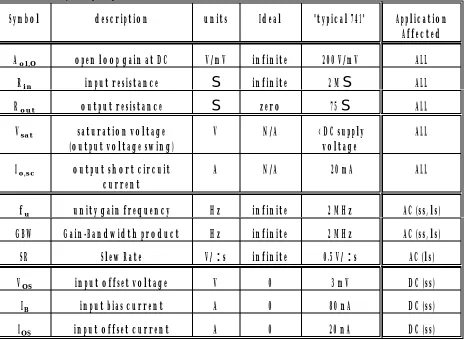
Table I lists the "non-ideal" characteristics of op-amps, the symbols, a short word description of each characteristic, and the typical units for the characteristic. (Note that there are no “standard” symbols referring to Op Amps.) Also included in Table I are values for an IDEAL op-amp, and, for comparison, the values listed in the 1988 National Semiconductor data book for a "typical" 741C op-amp. The final column in Table I indicates what type of application will be primarily affected by each characteristic.
The application "classes" used in this table are "DC", "AC", "ss", and "ls". In general, an op-amp application circuit will have elements of both. A DC application is one in which the relevant signals are "truly" DC or can be characterized as "slowly" varying in time, i.e., the values of the signals exhibit only gradual changes over time. For an AC application, the relevant signals can be described as sinusoidal in nature; this description also
includes any signals (including square waves) that can be described in terms of a Fourier series. The "ss" and "ls" symbols stand for small signal and large signal. For op-amp
TABLE 1: Summary of Op-Amp Characteristics
Symbol description units Ideal "typical 741" Application Affected
Aol,O open loop gain at DC V/mV infinite 200 V/mV ALL
Rin input resistance
S
infinite 2 MS
ALLRout output resistance
S
zero 75S
ALLVsat saturation voltage
(output voltage swing)
V N/A < DC supply voltage
ALL
Io,sc output short circuit
current
A N/A 20 mA ALL
fu unity gain frequency Hz infinite 2 MHz AC (ss, ls)
GBW Gain-Bandwidth product Hz infinite 2 MHz AC (ss, ls)
SR Slew Rate V/
:
s infinite 0.5 V/:
s AC (ls)VOS input offset voltage V 0 3 mV DC (ss)
IB input bias current A 0 80 nA DC (ss)
IOS input offset current A 0 20 nA DC (ss)
Questions:
1. What's the form of the "simplest" equivalent circuit for a (REAL) op-amp?
2. Based on the circuit of question 1, what values are assumed for the equivalent circuit parameters of an IDEAL op-amp?
3. How do you analyze an op-amp circuit in the presence of negative feedback? 4. Using the ideal op-amp model, determine the equation which expresses the
relationship between the output voltage and the input voltage for (a) an inverting amplifier; (b) a non-inverting amplifier; (c) a buffer amplifier; (d) a difference amplifier; (e) a differentiating amplifier; and (f) an integrating amplifier. For circuit drawings, see the schematics sheet entitled "Op-Amp Application Circuits: The Big Ten".
5. What is the significance of the supply voltage for an op-amp?
6. What is the relationship between the maximum output voltage swing and the supply voltage?
7. What is the relationship between maximum output voltage swing and the load resistance?
8. What is the significance of the output short circuit current? 9. Can a 741 op-amp (successfully) drive an 8
S
speaker directly? 10. What is the definition of unity gain frequency?13. What is the definition of slew rate?
14. What does "slew rate limiting" look like if the output voltage is a square wave? 15. What is the definition of "full power frequency", i.e., the maximum frequency at
which a sinusoidal output voltage will not be affected by the slew rate of the op-amp? What determines this full power frequency?
16. What does "slew rate limiting" look like if the output voltage is a sine wave? 17. What is the origin of (what is the cause of) the input offset current? 18. What is the origin of (what is the cause of) the input bias current?
19. In general, what type of op-amp will have larger values of IB and IOS, an op-amp with a
BJT differential input stage or an op-amp with an FET differential input stage? 20. In general, what type of op-amp will have larger values of VOS, an op-amp with a BJT
differential input stage or an op-amp with an FET differential input stage? 21. What's the definition of CMRR?
22. A 741C op-amp has a CMRR = 70 dB and a TL081C has a CMRR = 85 dB. Which op-amp would be best to use in an application intended to amplify a very low level input difference signal in the presence of significant common mode noise?
More Questions:
Here is another batch of questions. While we will answer many of these questions during the work for future Laboratories, you should start THINKING about appropriate answers to these questions NOW.
AC Error Sources and AC Application Circuits
1. What are the effects of the finite gain of the op-amp?
2. What are the effects of the bandwidth limitations of op-amps? A) Why doesn't an op-amp have an infinite bandwidth?
B) What is the definition of the unity gain frequency of an op-amp? C) What is the significance of the unity gain frequency of an op-amp? D) How does a designer minimize the effects of bandwidth limitation? E) How do the
:
A741, TL081 and TLE2037 op-amps compare with respect tobandwidth?
F) How would a designer choose which op-amp to use for a particular small signal amplifier application?
3. What are the effects of Slew-rate limitations?
A) What is the origin of slew-rate limiting in op-amps?
B) How does a designer minimize the effects of SR limitations?
C) How do the
:
A741, TL081 and TLE2037 op-amps compare with respect to Slew rate?D) How would a designer choose which op-amp to use for a particular large signal amplifier application?
DC Error Sources and DC Application Circuits. What are the effects of DC offset voltage, bias current and offset current?
1. Why do op-amps have a DC offset voltage?
4. How does a designer minimize the effects of the bias currents? 5. How does a designer minimize the effects of the offset currents?
6. How do the
:
A741, TL081 and TLE2037 op-amps compare with respect to DC offset characteristics?7. How would a designer choose which op-amp to use for a particular DC signal application?
References
To review IDEAL op-amps, good references include:
IRWIN, 3rd.ed., (your 011/012 text), Chapter 3, section 3.3, or HORENSTEIN (a previous 111 text), Chapter 2, or
SEDRA & SMITH, 3rd. ed., (current 111 text), Chapter 2, sections 0-6.
To review op-amp characteristics, good references include:
HORENSTEIN, Chapter 10, or
SEDRA & SMITH, 3rd.ed., Chapter 2, section 7 - 12,
PAYNTER, 3rd.ed., (an 010 text), Chapter 12, and section 13.6.
In addition to the specific references above, here are some other sources I used to develop my lecture notes. These additional references also are a source of "other" op-amp applications.
E.J. Kennedy, Operational Amplifier Circuits: Theory and Applications, Holt Rinehart Winston, New York, NY (1988).
Richard J. Higgins, Electronics with Digital and Analog Integrated Circuits, Prentice-Hall, Englewood Cliffs, NJ (1983).
Robert F. Coughlin and Frederick F. Driscoll, Operational Amplifiers and Linear Integrated Circuits, 4th ed., Prentice-Hall, Englewood Cliffs, NJ (1991).
Sergio Franco, Design with Operational Amplifiers and Analog Integrated Circuits, McGraw-Hill, New York, NY (1988).
J. Michael Jacob, Applications and Design with Analog Integrated Circuits, Reston Publishing (Prentice-Hall), Reston, VA (1982).
Linear 1 Databook, National Semiconductor Corporation, Santa Clara, CA (1988).
~~~~~~~~~~~~~~~~~~~~~~~~~~~~~~
Op-Amp Circuits Compendium
On the next two pages are some op-amp applications circuits". I call them the "BIG TEN", and "Variations on a Theme". Be able to recognize these circuits, so that if shown the circuit you can name it and derive the output/input relationship. If given the name of the circuit, you should be able to draw the appropriate topology. And if asked to design an op-amp application circuit, you should be able to have these circuits INSTANTLY available in the front of your brain.
For each circuit, be able to
1. Derive the appropriate output-to-input relationship.
2. Determine the input resistance of each circuit, where the input resistance is the resistance presented to the source by the circuit.
3. Determine the output resistance of each circuit, where the output resistance is the resistance presented to the load by the circuit.
Page 6 of 7
Page 7 of 7