warwick.ac.uk/lib-publications
Manuscript version: Author’s Accepted Manuscript
The version presented in WRAP is the author’s accepted manuscript and may differ from the
published version or Version of Record.
Persistent WRAP URL:
http://wrap.warwick.ac.uk/132228
How to cite:
Please refer to published version for the most recent bibliographic citation information.
If a published version is known of, the repository item page linked to above, will contain
details on accessing it.
Copyright and reuse:
The Warwick Research Archive Portal (WRAP) makes this work by researchers of the
University of Warwick available open access under the following conditions.
Copyright © and all moral rights to the version of the paper presented here belong to the
individual author(s) and/or other copyright owners. To the extent reasonable and
practicable the material made available in WRAP has been checked for eligibility before
being made available.
Copies of full items can be used for personal research or study, educational, or not-for-profit
purposes without prior permission or charge. Provided that the authors, title and full
bibliographic details are credited, a hyperlink and/or URL is given for the original metadata
page and the content is not changed in any way.
Publisher’s statement:
Please refer to the repository item page, publisher’s statement section, for further
information.
High Throughput Accelerator Interface Framework
for a Linear Time-Multiplexed FPGA Overlay
Xiangwei Li
∗, Kizheppatt Vipin
†, Douglas L. Maskell
‡, Suhaib A. Fahmy
§and Abhishek Kumar Jain
¶∗School of Electrical and Information Engineering, The University of Sydney, Australia †School of Engineering and Digital Sciences, Nazarbayev University, Kazakhstan ‡School of Computer Science and Engineering, Nanyang Technological University, Singapore
§School of Engineering, University of Warwick, United Kingdom ¶Xilinx Inc., United States
Abstract—Coarse-grained FPGA overlays improve design pro-ductivity through software-like programmability and fast com-pilation. However, the effectiveness of overlays as accelerators is dependent on suitable interface and programming integration into a typically processor-based computing system, an aspect which has often been neglected in evaluations of overlays. We explore the integration of a time-multiplexed FPGA overlay over a server-class PCI Express interface. We show how this integration can be optimised to maximise performance, and evaluate the area overhead. We also propose a user-friendly programming model for such an overlay accelerator system.
I. INTRODUCTION
The flexibility of FPGAs affords the significant benefits of custom hardware architectures with a level of flexibility not offered by ASICs. However, the compilation time from a hardware description to a bitstream is significant as a result of the fine-grained nature of the architecture and hence design tool complexity. Partial reconfiguration allows different accel-erators to be loaded dynamically at runtime but these must be designed in advance to generate partial bitstreams, and runtime compilation is not supported [1]. Hence, for more dynamic workloads, overlays have been proposed as an alternative approach. Coarse-grained overlays implemented on FPGAs enable faster compilation and software-like programmability because the coarse-grained to fine-grained mapping of the overlay is performed during the architecture design phase, optimising for the resources on the FPGA, and with a reg-ular structure. Mapping an application to this overlay then only requires description and compilation at a coarser grain, significantly simplifying the design process.
FPGA overlays can be broadly categorised as spatially configured (SC) or time-multiplexed (TM). In an SC overlay, a functional unit (FU) is allocated to a single computational operation in the accelerated kernel, with FUs connected by a routing network which is essentially static during execu-tion [2]. A TM overlay, on the other hand, shares both the FUs and the interconnect across kernel operations, allowing improved usage of the limited FPGA resource [3]. However, TM overlays suffer from relatively large area overheads, due to their underlying processor-like architecture [4], [5], [6], [7], [8] or, for CGRA-like overlays, due to the routing resources and instruction storage requirements [9], [10]. Reducing the area
overhead for CGRA-like overlays, specifically for the routing network, and utilizing their fast context switching capabilities is likely to result in improved usability with corresponding improvements in design productivity. A streaming architecture based on feed-forward pipelined datapaths, with a simple linear interconnect, was shown to drastically reduce hardware requirements [11]. However, performance analysis of such overlays often ignores the system interfacing aspects that are crucial to usability, as the interface between processor/memory subsystems and the overlay must be able to provide high-bandwidth, large scale data transmission. Existing FPGA interfacing frameworks fall into one of two categories, AXI bus-based solutions for FPGA SoC systems (like the Xilinx Zynq) and PCle-based solutions for integration into a host PC. Most AXI bus-based solutions are limited by the theoretical maximum bandwidth (400 MB/s) of the AXI Direct Memory Access (DMA) IP core [12], so PCIe-based interface frame-works are a better choice for overlay accelerators because of the much higher throughput.
In this paper, we implement overlay accelerator sys-tems with PCIe connectivity, based on the Xillybus [13], RIFFA [14] and DyRACT [15] frameworks. The architecture of the TM overlay and its essential control are presented, along with a full working implementation integrated into the memory subsystem. The PCIe-based overlay accelerators are evaluated for a range of benchmarks to determine the most suitable interface in terms of its supporting configuration and streaming through the overlay.
II. RELATEDWORK
A. Coarse-grained TM Overlays
A number of overlays have been proposed which share functional units among kernel operations in an attempt to reduce overlay resource requirements [4], [10], [16]. This time-multiplexing of the overlay means it can change its behavior on a cycle-by-cycle basis while the compute kernel is executing, better sharing the limited FPGA resources.
the processor and the reconfigurable array compared to tradi-tional CGRAs. Taras [16] implemented ADRES on Intel and Xilinx FPGAs using the CGRA-ME modeling framework [18]. QuickDough [10] consists of an array of nearest neighbor interconnected processing elements (PEs), referred to as the SCGRA overlay. The 250 MHz FU consists of an ALU, multiport data memory (256×32 bits) and customizable depth instruction ROM (Supporting 72-bit instructions) resulting in significant BRAM utilization, which limits its scalability. Only a5×5 array can fit on the Xilinx Zynq, along with a significant frequency degradation caused by the tight placement and routing.
VectorBlox MXP [4] is a commercial soft vector processor overlay targeting Altera or Xilinx FPGAs via the Avalon or AXI interfaces. Data transfer is handled by a double-buffered vector scratchpad and a dedicated DMA engine communicat-ing with the scalar host processor via the AXI HP port. MXP can operate at a maximum frequency of 110 MHz on a Xilinx XC7Z020 device with 16 vector lanes [19]. It demonstrates up to1000×speedup over MicroBlaze. The programming model is a combination of ANSI-C and VectorBlox C extensions. However, it is difficult to implement applications which cannot be easily vectorized.
B. PCIe-based Accelerator Interfacing Frameworks
Northwest Logic [20] and Xillybus [13] are two repre-sentative commercial solutions which support PCIe interfaces for different generations while providing portability across different FPGA devices. Northwest Logic is a licensed closed source while Xillybus is provided free of charge for research and teaching purposes. Xillybus users have full access to the source code, with good documentation provided. The latest version of Xillybus (Revision XL) can achieve a maximum data rate of ∼3.5 GB/s for Gen 2×8 PCIe interfaces.
RIFFA [14] is an open source framework for the integration of FPGA accelerators supporting PCIe Gen 2 and Gen 3 standards. A scatter-gather DMA-based design bridges the vendor-specific PCIe endpoint core and multiple communi-cation channels for user defined IP cores. The latest RIFFA release (V2.2.2) achieves a unidirectional maximum band-width of 3.6 GB/s for the Gen2×8 configuration on the Xilinx VC707 platform and 3.5 GB/s for the Gen3×4 configuration on the Terasic DE5-Net. DyRACT [15] focuses on dynamic partial reconfiguration over the PCIe Gen2×4 interface, along with a configuration controller and clock management. Other solutions include, EPEE [21] which is a general purpose PCIe communication library, targeting a wide range of FPGA devices, and JetStream [22] which is a PCIe Gen3 solution supporting not only FPGA-to-Host communication but also multi-FPGA interfacing.
Although overlays have shown potential in improving FPGA design productivity, few of them have been developed as full accelerator systems. Among the existing PCIe implementa-tions, Xillybus, RIFFA and DyRACT appear to be the most promising solutions due to their availability, ease-of-use and
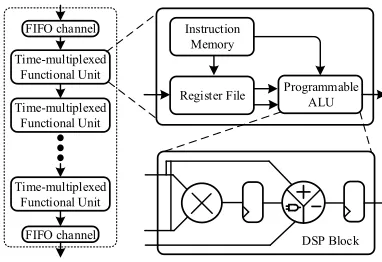
Time-multiplexed Functional Unit
FIFO channel
Time-multiplexed Functional Unit
Programmable ALU Register File
Instruction Memory
DSP Block Time-multiplexed
Functional Unit
[image:3.612.341.532.53.184.2]FIFO channel
Fig. 1: A linear TM overlay.
portability. In subsequent sections we explore these solutions and analyse overlay capabilities with these interfaces.
III. LINEARTM OVERLAY
A. Architecture Description
A 32-bit TM overlay with a linear array of FUs is used to develop the accelerator system, similar to the design in [11], where each FU can be time multiplexed among operations present in a single scheduling stage of a directed acyclic graph (DAG). It consists of a quasi-streaming data interface made up of two FIFO channels implemented using Block RAMs, which transmit data through daisy-chained fully pipelined TM FUs, as in Fig. 1. By eliminating the fully flexible routing of CGRA-like overlays, this structure achieves a much more area-efficient design, using fewer than 6% of the logic and DSP resources on a Xilinx Zynq device. The initiation interval (II) [23] can be significantly reduced by making minor architectural enhancements, such as adding a rotating register file and replicating the data stream. These changes result in a peak throughput of 1.8 GOPS with a frequency of 335 MHz. Adding write-back to the FU design reduces the overlay depth requirement by allowing multiple nodes on the critical path to be combined. This also eliminates the need to reconfigure the overlay when the application kernel changes, making the overlay suitable for more general purpose applications.
B. Overlay Control
A back-pressure control circuit is built around the input FIFO channel to manage overlay functionality, as in Fig. 2. There are three control signals, inst load, reg wren, and
Input FIFO Channel
empty
counter rd_en
data_in
data_out valid_out inst_load
data_wren
instruction
full
reg_wren reg_in
[image:4.612.51.304.50.137.2]wr_en
Fig. 2: Back-pressure control circuit.
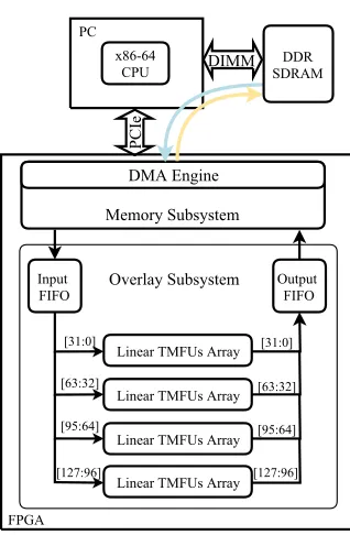
Memory Subsystem
FPGA
Linear TMFUs Array Input
FIFO Output FIFO
Linear TMFUs Array
Linear TMFUs Array
Linear TMFUs Array
[image:4.612.94.253.161.404.2][31:0]
[63:32]
[95:64]
[127:96]
[31:0]
[63:32]
[95:64]
[127:96]
DMA Engine
Overlay Subsystem
PCIe
x86-64 CPU PC
DDR SDRAM
DIMM
Fig. 3: The proposed overlay accelerator system.
In Fig. 2, the left dashed box is the control for the write enable port of the FIFO, while the right dashed box contains the logic to control the FIFO read enable port. Data is written into the FIFO when wr en is high. The FIFO read enable signal (rd en) is generated using a counter which starts from 0 when the emptysignal goes low (indicating that FIFO data is available). The counter counts up until II−1, at which point it rolls over back to zero. This repeats until the amount of data matches the number written to the back-pressure controller.
IV. OVERLAYACCELERATORFRAMEWORK
The linear TM overlay is area efficient, with fast con-text switching and high throughput [11]. However, a high-bandwidth PCIe interface between the processor/memory sub-system and the overlay is required to fully demonstrate the FPGA accelerator, as shown in Fig. 3. Register access is also required so that the user can control the overlay system, i.e. perform instruction load, overlay setup, and data write. To make full use of PCIe’s 128-bit data bandwidth we replicate four 32-bit linear TM overlays, which can then run four kernel instances at runtime, reducing the II to a quarter that of a single overlay. Data transfers between the internal memory subsystem and the DDR SDRAM are under DMA control.
TABLE I: Example code.
fpga_reg_wr(0x30,0x0); //Tag of FU0
fpga_reg_wr(0x34,0x3033D080); //Instruction 0
fpga_reg_wr(0x30,0x1); //Tag of FU1
fpga_reg_wr(0x34,0x8852000); //Instruction 1
fpga_reg_wr(0x38,5); //No. of input data
fpga_reg_wr(0x38,5); //(II-1)
dyract_send_data((unsigned char *)mydata, sendSize*sizeof( int)); //Send data
dyract_recv_data((unsigned char *) recvdata, recvSize* sizeof(4)); //Receive data
A. System Integration
FIFO connections controlled by the back-pressure circuit are used between the TM overlay and PCIe interface. Taking DyRACT as an example, the original version was modified to support the proposed overlay architecture. DyRACT orig-inally used high-speed PCIe communication between a host computer and user logic on FPGA to provide support for partial reconfiguration (PR). It also provided multiple AXI4-stream backend interfaces for seamless integration with vendor supplied IP cores. As we do not need PR, the reconfiguration control logic is disabled, and a single AXI4-stream interface is enabled, configurable through width-conversion FIFOs. A new AXI-Lite interface is added to support the command-data interface between the host and the overlay. The low-level communication protocols and interrupts are managed by the driver and the user library provides APIs for integration with application programs.
B. Programming Model
Xillybus and RIFFA provide RTL design along with driver support and software code demos, but generally do not have direct access to the FPGA RAMs. However, DyRACT allows register access via the AXI-Lite interface. Thus, the user can send the instructions and streaming data from the PC to the FPGA at runtime via dedicated APIs, instead of reconfiguring the overlay. In the modified DyRACT system, three registers are provided for overlay control. One register (0x30) is written with a 4-bit tag, which is followed by a write to register 0x34 to store an instruction into its corresponding FU. Register 0x38 is used to store the number of data words to be input to the first FU for a specific compute kernel (determined based on the instructions and the II). Next, user data is transferred to the overlay, processed, and then sent back to the host PC. An example code snippet (Table I) shows how to load the instructions, set up the overlay and write the data to the FPGA.
V. EXPERIMENTALEVALUATION
TABLE II: DFG characteristics of benchmark set.
No. Benchmark
Characteristics
I/O graph op graph graph
nodes edges nodes depth width
1. chebyshev 1/1 12 7 7 1
2. mibench 3/1 22 13 6 3
3. qspline 7/1 50 25 8 6
4. fft 6/4 24 10 3 4
5. kmeans 16/1 39 23 5 8
6. mm 16/1 31 15 4 8
7. spmv 16/2 30 14 4 8
8. stencil 15/2 30 14 5 6
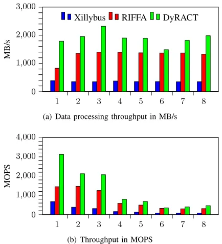
clocked at the maximum frequency (250 MHz). The Xillybus and RIFFA accelerators required that FU instructions are hard-coded as they have no direct access to the FPGA RAMs, thus requiring that the overlay is reconfigured when the application kernel changes. In comparison, the DyRACT accelerator can write to FPGA memory to modify the FU instructions (along with the tags), the amount of input data and the value of II-1. Fig. 4 shows the performance of the four 32-bit linear TM overlays integrated with Xillybus, RIFFA and DyRACT. The Xillybus and DyRACT accelerators use a block size of 1M words, while the RIFFA accelerator uses a block size of 128K words. Fig. 4(a) shows that the DyRACT accelerator achieves an average throughput of 1892 MB/s, which is≈45% higher than the RIFFA accelerator (average throughput of 1300 MB/s) and 5.3×better than the Xillybus accelerator (average throughput of 358 MB/s). These system ratios are roughly maintained when the overlay throughput is examined in terms of mega-operations per second (MOPS). All three accelerators show only slight differences in the throughput, in MB/s, for the various applications. However, there are large differences when the throughput is presented in terms of overlay MOPS. This is mainly related to the number of I/O nodes in the application, which results in larger II values and thus reduced throughput. Thus, the linear TM overlay accelerators are more suitable to the benchmarks which have fewer I/O ports.
Table III shows the FPGA resource usage of the Xilly-bus, RIFFA and DyRACT based systems, respectively. The Xillybus based system consumes the fewest FFs (33% fewer than the RIFFA based system), while the RIFFA based system requires the least number of LUTs (20% fewer than the DyRACT based system). The DyRACT based system is the most area efficient in terms of BRAM consumption (96% fewer than the RIFFA based system). While the logic and DSP resources used are comparable among all these imple-mentations, there is a big difference in the BRAM utilization specifically for the RIFFA based system. This is due to the half-duplex operating mode of the RIFFA interface, which requires a large number of BRAMs to implement the two large depth FWFT FIFOs. Developing a full-duplex RIFFA based system would minimize the BRAM resource usage. Currently, the DyRACT and Xillybus based systems are more efficient in terms of area than the RIFFA based system.
1 2 3 4 5 6 7 8
0 1,000 2,000 3,000
MB/s
Xillybus RIFFA DyRACT
(a) Data processing throughput in MB/s
1 2 3 4 5 6 7 8
0 1,000 2,000 3,000 4,000
MOPS
[image:5.612.69.286.66.188.2](b) Throughput in MOPS
[image:5.612.328.548.341.430.2]Fig. 4: Performance comparison for the benchmarks.
TABLE III: Area overhead of PCIe-based systems.
System Resource Usage
LUTs FFs BRAMs DSPs
Xillybus 16,027 12,488 14.5 32
RIFFA 13,657 18,581 289.5 32
DyRACT 17,029 16,302 10 32
Available 303,600 607,200 1,030 2,800
VI. CONCLUSIONS
In this paper, we have proposed high-performance overlay accelerator systems based on a number of PCIe interfaces, i.e. Xillybus, RIFFA and DyRACT. The DyRACT based system has a 5.3× speed improvement when compared to the Xillybus based system, and a 45% better throughput than the RIFFA based system, achieving a throughput of 1892 MB/s on average. Currently, the DyRACT based system is the most promising overlay accelerator, as it provides the best data throughput with the least BRAM utilisation and comparable LUT and FF consumption. Furthermore, it has a simple programming model thus avoiding overlay recon-figuration whenever a compute kernel changes. Xillybus and DyRACT are full-duplex implementations, and implementing a full-duplex RIFFA based system would not only reduce its BRAM utilization but also potentially improve the throughput, although this is left for future work.
ACKNOWLEDGMENT
REFERENCES
[1] K. Vipin and S. A. Fahmy, “FPGA dynamic and partial reconfiguration: A survey of architectures, methods, and applications,”ACM Computing
Surveys, vol. 51, no. 4, pp. 72:1–72:39, 2018.
[2] A. K. Jain, D. L. Maskell, and S. A. Fahmy, “Throughput oriented FPGA overlays using DSP blocks,” inProceedings of the Design, Automation
and Test in Europe Conference (DATE), 2016, pp. 1628–1633.
[3] X. Li and D. L. Maskell, “Time-multiplexed FPGA overlay architectures: A survey,” ACM Transactions on Design Automation of Electronic
Systems, vol. 24, no. 5, pp. 54:1–54:19, 2019.
[4] A. Severance and G. G. Lemieux, “Embedded supercomputing in FPGAs with the VectorBlox MXP matrix processor,” in Proceedings of the International Conference on Hardware/Software Codesign and System
Synthesis (CODES+ ISSS), 2013.
[5] R. Rashid, J. G. Steffan, and V. Betz, “Comparing performance, produc-tivity and scalability of the TILT overlay processor to OpenCL HLS,”
inProceedings of the International Conference on Field Programmable
Technology (FPT), 2014, pp. 20–27.
[6] M. Al Kadi, B. Janssen, and M. Huebner, “FGPU: An SIMT-architecture for FPGAs,” inProceedings of the International Symposium on Field
Programmable Gate Arrays (FPGA), 2016, pp. 254–263.
[7] J. Gray, “GRVI-Phalanx: A massively parallel RISC-V FPGA ac-celerator,” in Proceedings of the International Symposium on Field
Programmable Custom Computing Machines (FCCM), 2016, pp. 17–
20.
[8] P. Duarte, P. Tomas, and G. Falcao, “SCRATCH: an end-to-end application-aware soft-GPGPU architecture and trimming tool,” in
Pro-ceedings of the International Symposium on Microarchitecture, 2017,
pp. 165–177.
[9] K. Paul, C. Dash, and M. S. Moghaddam, “reMORPH: a runtime re-configurable architecture,” inProceedings of the Euromicro Conference
on Digital Systems Design (DSD), 2012, pp. 26–33.
[10] C. Liu, H.-C. Ng, and H. K.-H. So, “QuickDough: a rapid FPGA loop accelerator design framework using soft CGRA overlay,” inProceedings of the International Conference on Field Programmable Technology
(FPT), 2015, pp. 56–63.
[11] X. Li, A. K. Jain, D. L. Maskell, and S. A. Fahmy, “A time-multiplexed FPGA overlay with linear interconnect,” inProceedings of the Design,
Automation and Test in Europe Conference (DATE), 2018, pp. 1075–
1080.
[12] Xilinx Ltd. AXI DMA v7.1 LogiCORE IP Product Guide. [Online]. Available: www.xilinx.com
[13] Xillybus Ltd., “IP core product brief.” [Online]. Available: https: //www.xillybus.com
[14] M. Jacobsen, D. Richmond, M. Hogains, and R. Kastner, “RIFFA 2.1: A reusable integration framework for FPGA accelerators,”ACM
Transactions on Reconfigurable Technology and Systems, vol. 8, no. 4,
p. 22, 2015.
[15] K. Vipin and S. A. Fahmy, “DyRACT: A partial reconfiguration enabled accelerator and test platform,” in Proceedings of the International
Conference on Field Programmable Logic and Applications (FPL),
2014.
[16] I. Taras and J. H. Anderson, “Impact of FPGA architecture on area and performance of CGRA overlays,” in Proceedings of the Interna-tional Symposium on Field-Programmable Custom Computing Machines
(FCCM), 2019, pp. 87–95.
[17] B. Mei, S. Vernalde, D. Verkest, H. De Man, and R. Lauwereins, “ADRES: An architecture with tightly coupled VLIW processor and coarse-grained reconfigurable matrix,” in Proceedings of the Inter-national Conference on Field Programmable Logic and Applications
(FPL), 2003, pp. 61–70.
[18] S. A. Chin, N. Sakamoto, A. Rui, J. Zhao, J. H. Kim, Y. Hara-Azumi, and J. Anderson, “CGRA-ME: a unified framework for CGRA modelling and exploration,” inProceedings of the IEEE International Conference
on Application-specific Systems, Architectures and Processors (ASAP),
2017, pp. 184–189.
[19] S. J. Jie and N. Kapre, “Comparing soft and hard vector processing in FPGA-based embedded systems,” inProceedings of the International
Conference on Field Programmable Logic and Applications (FPL),
2014.
[20] Northwest Logic Inc., “PCI Express solution overview.” [Online]. Available: https://nwlogic.com/products/pci-express-solution/
[21] J. Gong, T. Wang, J. Chen, H. Wu, F. Ye, S. Lu, and J. Cong, “An efficient and flexible host-FPGA PCIe communication library,” in
Proceedings of the International Conference on Field Programmable
Logic and Applications (FPL), 2014.
[22] M. Vesper, D. Koch, K. Vipin, and S. A. Fahmy, “JetStream: An open-source high-performance PCI express 3 streaming library for FPGA-to-Host and FPGA-to-FPGA communication,” inProceedings of the In-ternational Conference on Field Programmable Logic and Applications
(FPL), 2016.
[23] M. Lam, “Software pipelining: An effective scheduling technique for VLIW machines,” in ACM Sigplan Notices, vol. 23, no. 7, 1988, pp. 318–328.
[24] S. Gopalakrishnan, P. Kalla, M. B. Meredith, and F. Enescu, “Finding linear building-blocks for RTL synthesis of polynomial datapaths with fixed-size bit-vectors,” inProceedings of the International Conference
on Computer Aided Design (ICCAD), 2007, pp. 143–148.
[25] C.-H. Hoy, V. Govindarajuz, T. Nowatzki, R. Nagaraju, Z. Marzecy, P. Agarwal, C. Frericks, R. Cofell, and K. Sankaralingam, “Performance evaluation of a DySER FPGA prototype system spanning the compiler, microarchitecture, and hardware implementation,” in Proceedings of the International Symposium on Performance Analysis of Systems and