Comparative Analysis and Design of Different Type
of Low Power High Speed Dynamic Double Latch
Comparator using H-Spice and CMOS Technology
Babita1, Sunaina2
1
M.Tech Scholar, ECE Department, Indus Institute of Engg. And Technology-Jind, 126102, India
2
Assistant professor, ECE Department, Indus Institute of Engg. And Technology-Jind, 126102, India
Abstract: Now-a-days power generation is a big problem. To achieve the power consumption scaling is important in all circuits. Comparator is one of the components most importantly required in Analog to digital converter. In this research we present a comparative analysis of high speed dynamic comparator in a scaling ranges such as 180nm. A comparison can be performed among various circuit parameters. The main parameters considered in the performance analysis are delay and power consumption. H-Spice simulation software is used for design and analysis of the dynamic comparator circuits in the above specified scaling range. Finally functionality of the proposed comparator is checking via Quatrus Kit in Verilog coding. Double-tail comparator that is used to examine analog signal to give digital output is proposed. Proposed double Double-tail comparator makes use of power gating technique for energy reduction and delay discount. New electricity gating double tail comparator gives 15% discount in power in addition to 71% discount in kickback noise the new design is simulated in TSMC180nm in Tanner tool which can be measured to determine electricity dissipation, pace and kickback noise. these are compared with preceding designs. This paper provides an excessive overall performance, low strength dynamic latch comparator utilizing strength gating method for the cause of reduced electricity. The comparator has usually been a coronary heart of analog to virtual converters in VLSI circuits. The reduction in energy intake of comparator ultimately reduces the power consumption in ADC blocks. The proposed design has been simulated on Tanner EDA at 180nm TSMC and executed up to 15% discount in strength and discount on kickback noise from the traditional designs and based on the present effects and evaluation. a new low power, high performance comparator is proposed, in which the circuit of a dynamic double-tail comparator.
Keywords:VLSI circuits, ADC blocks, double-tail comparator, H-Spice simulation software.
I. INTRODUCTION
Evaluation is an often-used operation in special good judgment and arithmetic programs. it is also required in threshold features and cells like feel amplifiers. The primary feature of a comparator is to compare an analog signal with every other analog signal or reference and output a binary sign primarily based on contrast. considering that it's miles less difficult to distribute voltages to a large quantity of comparators than to distribute currents, maximum converters appoint voltage evaluation. A voltage comparator can be virtually seemed as a 1-bit ADC. On this painting, we will be accomplishing an examine of various comparator topologies with them deserves/demerits and packages. The simulation of a comparator may also be accomplished with the assist of SPICE to investigate the circuits and calculate the performance parameters like postpone, enter variety, strength consumption and so on. A comparator is a tool that compares two voltages or currents and outputs a virtual signal indicating which is larger. Comparator is a circuit that compares one analog signal with every other analog signal or a reference voltage and outputs a binary signal based totally on the comparison and works on phases: reset and regeneration phase. It is a completely crucial element of an analog to virtual converter (ADC). Analog to digital converter is a tool that converts a continuous bodily quantity (normally voltage) to a virtual range. The conversion involves quantization of input, so it necessarily introduces a small amount of errors. it is an iterative method. The inverse operation is carried out through a virtual to analog converter (DAC).
A. Differential Voltage
B. Static Characteristics
A comparator became described above as a circuit that has a binary output whose value is based totally on an evaluation of two analog inputs. that is illustrated in Fig.1.l As proven on this figure. The output of the comparator is excessive (VOH) whilst the difference between the no inverting and inverting inputs is superb, and coffee (VOL) when this difference is bad. despite the fact that this type of behavior is not possible in a real-world state of affairs, it can be modeled with perfect circuit factors with mathematical descriptions. One such circuit version is proven in Fig.2.2 contains a voltage-managed voltage source (VCVS) whose characteristics are defined the mathematical system given at the figure.
Vo=VOH,For (Vp-Vn>0)
Vo=VOL,For(Vp-Vn<0)
[image:2.612.248.368.168.311.2]Vo=VOH=VOL For (Vp-Vn=0)
Figure 1.l Ideal transfer curve
C. Single tail comparator
The Circuit diagram of the Single tail comparator is shown in Fig.1.2 It is mostly used in A/D converters, with high input impedance, no static power dissipation and rail-to-rail ouput swing.
Fig 1.2 Single tail comparator
[image:2.612.217.403.394.582.2]D. Differential Pair Comparator
Figure 1.3 Differential Pair Comparator-Latch Type
The operation of the comparator can be honestly described as follows. During reset phase (Clock=0V), Out nodes of the pass-coupled inverters (M6-M9) are reset to VDD through the reset transistors M4 and M5. at some stage in assessment phase (Clk=VDD), the tail transistor Ml isturned on at the rising Clk edge. The input transistor pair (M2 and M3) starts off evolved to discharge each Di node voltage with a special time fee proportional to the every carried-out input voltage from VDD to 0V. as soon as both of Di node voltages drops round VDD−Vtn, then the NMO Stransistors of the move-coupled inverters M6 and M7 turn on and these initiates the positive feedback. as soon as either of Out node voltage reaches around, the PMOS transistors of the inverters M2 and M4 also switch on; further improving the nice comments and enabling the regeneration of a small differential voltage
ΔVinto a complete swing differential output. comparing with Lewis-grey comparator, this comparator suggests faster operation and less average offset voltage. but, nonetheless its structure which consists of a stack of 4transistors calls for massive voltage headroom; it's miles intricate in low-voltage deep-submicron CMOS technologies. moreover, that allows you to boom the force currents of the latch, it is inevitable to length up the transistor Ml given that this comparator has simplest one tail transistor Ml.
II. LITERATURE REVIEW
Chandra hash Patel et.al, June 20l4 [l] described that a comparator is a device that compares voltages or currents and outputs a virtual sign indicating which is bigger. Comparator is a circuit that compares one analog signal with another analog sign or a reference voltage and outputs a binary signal based at the assessment and works on two stages: reset and regeneration phase. B. Wichtet.al ,2014 [9] analyzed impact of supply voltage, input dc degree, transistor sizing, and temperature at the enter offset. The sense amplifier is rapid in decision making due to sturdy tremendous remarks. There ought to not be static power dissipation when circuit is idle however that is tough to implement. to triumph over this hassle a decoupling resistor is used. the usage of this technique results in lower pace.
V.Kowsalya, 20l4 [24] defined that clock gating is a today's approach used in many synchronous circuits for lowering dynamic electricity dissipation. Clock gating saves power with the aid of including more common sense to a circuit to reduce the clock tree. Pruning the clock disables portions of the circuitry in order that the turn-flops in them do now not have to switch states. Switching states consumes strength. whilst no longer being switched, the switching electricity consumption is going to 0, and best leakage currents are incurred. The Comparators are utilized in analog-to-digital converters (ADCs), statistics transmission programs, switching power regulators and plenty of different programs.
R. Lotfi et.al .2013 [8] proposed a new comparator to conquer the downside of huge strength consumption. In a completely-differential pipelined analog-to-digital converter, the comparators ought to be able to compare a fully-completely-differential sign with a rail-to-rail swing with a completely-differential reference voltage any other advantage of the proposed architecture is that it is able to be implemented in a pure virtual process as it employs most effective MOS transistors.
III. CONVENTIONAL COMPARATORS
A. Characterisation Of Comparator
A tremendous voltage applied on the Vp enter will reason the comparator output to move nice, while a wonderful voltage applied on the Vn input will reason the comparator output to go terrible. The higher and lower voltage limits of the comparator Output are defined as VOH and VOL respectively.
1) Static Characteristics: A comparator became defined above as a circuit that has a binary output whose value is based on a comparison of two analog inputs. this is illustrated in Fig.3. l. The output of the comparator is high when the distinction between the non-inverting and inverting inputs is superb, and low while this difference is negative. despite the fact that this type of behavior is not possible in a actual-global scenario, it may be modeled with best circuit elements with mathematical descriptions. One such circuit model is proven in Fig.3.l accommodates a voltage-managed voltage source whose characteristics are defined the mathematical formula given at the discern. As CMOS generation scaling down, low-strength design becomes a important priority for gadgets. on the other hand, the deliver voltage is dramatically decreased. virtual incorporated circuits designs can fully enjoy the continuing down-scaling of CMOS processes as well as from the ongoing reduction of deliver voltage. In assessment to digital incorporated circuits designs, analog included circuits frequently can not be designed with minimal duration components for motives of advantage, offset, and many others. both analog and virtual circuit designers face unique demanding situations to design high performance circuitry with low electricity concerns. digital designers have to compete with such troubles as good judgment strategies (dynamic versus static as opposed to bypass-gate, etc.), threshold voltage scaling, strength-down techniques and most significantly, electricity deliver scaling.
Fig.3.l Ideal transfer curve of a comparator
2) Dynamic Characteristics : The dynamic characteristics of the comparator include both small-sign and large-signal conduct. We do now not recognize, at this factor, how long it takes for the comparator to respond to the given differential enter. The function delay between input excitation and output transition is the time response of the comparator. there's a postpone between the input excitation and the output response. This• time distinction is known as the propagation put off time of the comparator. it's miles a totally important parameter considering it's far often the rate dilemma inside the conversion charge. The propagation put off time in comparators commonly varies as a function of the amplitude of the input. a larger input will result in a smaller postpone time. there is an upper restrict at which a further increase in the input voltage, will not affect the postpone. This mode of operation is referred to as slewing or slew price.
B. Traditional Comparator
discharge with different discharging charges depending at the corresponding input voltage (motel/INP). Assuming the case in which VINP > VINN, Outp discharges faster than Outn, therefore while Outp (discharged through transistor M2 drain current), falls all the way down toVthpearlier than Outn (discharged by transistor Ml drain modern-day), the corresponding P-MOS transistor (M5) will turn on beginning the latch regeneration resulting from returned-to-lower back inverters (M3, M5 and M4, M6). accordingly, Outn pulls to VDD and Outp discharges to ground. If VINP < VINN, the circuits paintings vice versa.
C. Double Tail Comparator
The operation of this comparator is as follows (Fig3.5). at some point of reset segment (CLK = 0, M-tail1, and Mtail2 are off), transistors M3-M4 pre-rate fn and fp nodes to VDD, which in turn causes transistors MRl and MR2 to discharge the output nodes to floor. at some point of selection-making segment (CLK = VDD, M-tail1 and M-tail2 switch on), M3-M4 flip off and voltages at
nodes fn and fp start to drop with the fee defined by using IM-tail1/C fn(p) and on top of this, an enter-dependent differential voltage Vfn(p) will increase. The intermediate level fashioned with the aid of MR1 and MR2 passes Vfn(p) to the move coupled inverters and also offers an excellent protective among enter and output, ensuing in reduced fee of kickback noise. After the firstn-channel transistor of the latch activates (as an instance, M9), the corresponding output (e.g., Outn) will be discharged to the ground, leading the front p-channel transistor (e.g., M8) to turn on, charging some other output (Outp) to the deliver voltage (VDD). on this comparator, both intermediate degree transistors might be sooner or later cut-off, (due to the fact fn and fp nodes both discharge to the ground), subsequently they do now not play any function in improving the powerful trans conductance of the latch. besides, for the duration of reset section, these nodes have to be charged from ground to VDD, which means energy consumption.
IV. PROPOSED LATCHDYNAMIC COMPARATOR
A. Operation Principles of Proposed Comparator
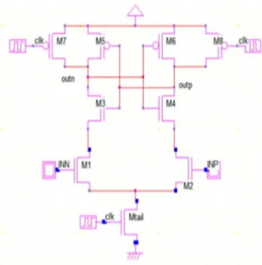
[image:5.612.213.400.540.719.2]This Fig.4.l shows the schematic layout of proposed comparator it's miles designed by means of the usage of TANNER EDA tool. The schematic and simulated waveforms of the proposed comparator are proven in Fig 4.l and 4.2. The circuit is designed and simulated with TANNER EDA using l80nm generation document and the layout and simulation conditions are VDD=l.8VTherefore, the proposed comparator offers higher input offset characteristic and faster operation similarly to the benefits of these comparators which include much less kickback noise, reduced clock load and removal of the timing requirement between Clk and Clk’ over a wide commonplace-mode and supply voltage range. For its operation, at some point of the reset segment, whilst Clk=zero, M-tail1&M-tail2 are off,M3 & M4 transistors gets on and charge the fp and fn nodes to Vdd,through out this time Mcl&Mc2 transistors are cut off. Then Mrl& Mr2 intermediate transistors reset latch output to ground. In the course of the choice-making phase, while Clk=Vdd, M-tail1& M-tail2 Transistors are on and M3&M4 transistors are off.At the start of phase, the Mcl&Mc2 transistors are nonetheless off. in line with input voltge the fp&fn nodes begin discharging with unique prices. If Vinp>Vinn,then fp node discharge faster than fn node, which causes the Mc2 transistor switch on, recharge fp node to vdd and Mc2 transistor will remain in off role and vice versa. within the proposedidea, one of the manipulate transistorsMcl activates,a modern-day from vdd is drawn to groundMcl,Ml,Mswl,Mtail1 which ends in static strength intake. Even the switching transistor Mswlcannot completely lessen the trouble of static electricity
In proposed double-tail comparator we kept all transistor sizing same. while for modification purpose and to reduce, parameters where we remove cross coupled transistor near clock. as they are used for only speedup the latch operation but presence of which increases power in our circuit. for power and delay reduction here were use power gating technique where we add one pomes in parallel with upper tail with small duration of clock and one extra nose transistor in bottom tail. for further reduction in kickback noise we add one capacitor at each input side of very small value which is charge on very small value of voltage and pass maximum voltage to circuit for its operation. By adding the comparator well-positioned capacitors of proper value at input side NMOS, the analysis guides the design of a robust synchronized kickback noise cancellation technique, eliminating those unwanted charges at the gate of the input MOS pair at different time intervals., restraining the voltage variation at the inputs due to different operation regions of the MOS devices. Which intern drastically reduce our kickback noise in circuit.
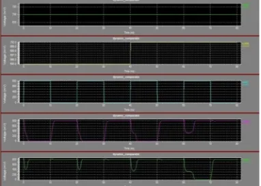
Fig.4.2 Transient response of proposed comparator
Hysteresis is the quality of the comparator in which the input threshold changes as a function of the input (or output) level. In particular, when the input passes the threshold, the output changes and the input threshold is subsequently reduced so that the input must return beyond the previous threshold before the comparator's output changes state again.
V. COMPARATOR ANALYSIS
Tanner software program is used for simulation. if you want to evaluate the proposed comparator with unmarried tail comparator and double tail traditional comparator. All comparator has been simulated in 0.l8um CMOS era with Vdd=0.8v. The put off &electricity consumption of proposed comparator is appreciably reduced.
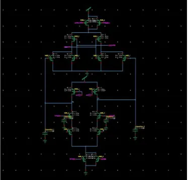
in this bankruptcy, we have provided the simulation and evaluation results of all comparator as provided in previous chapter. The double tail comparator has a proposed structure which reduces put off by means of growing latch regeneration velocity. The simulated comparator consists of additional move coupled transistors at enter, which isn't like conventional double tail comparator and will increase speed. The schematic of the simulated comparator is shown beneath. The layout has been applied and analyzed in Tanner suit. The schematic of the circuit drawn in S-Edit is proven below.
A. Kickback Noise:
It's miles feasible to decide the dimensions of those transistors in a way that maintains the advantages of the speed enhancement and energy discount, at the same time as reducing kickback noise. except, for some packages wherein kickback turns into crucial, it is feasible to use easy kickback discount strategies, which include neutralization to remarkably lessen the kickback noise.
B. Put off Analysis
It allows you to theoretically reveal how the postpone is decreased, delay equations are derived for this structure aspreviously done for the traditional dynamic comparator and the traditional double-tail dynamic comparator. The evaluation is similar to the conventional double-tail dynamic comparator, but; the proposed dynamic comparator complements the speed of the double-tail comparator by affecting vital elements: first, it increases the initial output voltage difference (V0) at the beginning of the
regeneration (t = t0); and 2d, it enhances the effective transconductance (gmeff) of the latch. each of these elements might be
discussed in detail.
1) Effect of EnhancingV0: As mentioned earlier than, we outline t0, as a time after which latch regeneration starts offevolved. In
different phrases, t0 is considered to be the time it takes (whilst each latch outputs are rising with specific costs) till the primary
NMOS transistor of the back-to-again inverters activates, with the intention to pull down one of the outputs and regeneration will begin. Thelatch output voltage distinction at time t0, (V0) has a significant impact at the latch regeneration time, such that
bigger V0 outcomes in much less regeneration time
2) Impact of enhancing latch powerful Tran conductance: As stated before, in conventional double-tail comparator, both fn and fp nodes will be subsequently discharged completely. In our proposed comparator, however, the fact that one of the first stage output nodes (fn/fp) will feed up lower back to the VDD at the beginning of the decision-making section, will switch on one of the intermediate degree transistors, accordingly the effective.
[image:7.612.218.396.363.549.2]C. Dynamic Comparator
Figure 5.1:Schematic Diagram Dynamic Comparator
[image:7.612.212.403.579.715.2]Figure5.3: Analysis and Result of Dynamic Comparator
D. Base Double-Tail Comparator
Figure 5.4: Schematic Diagram of Double Tail Comparator
VI. CONCLUSION AND FUTURE WORK
A. Conclusion
B. Future Work
The same structures can be implemented by using FINFET to further improve the functionality of the circuit. As noted earlier, since the proposed fully dynamic latched comparator can be optimized for either the minimal kickback noise voltage or the maximum load drivability at a restricted area in line with the layout specification, trying to find the most suitable utility may be one subject matter for the future works. similarly, kickback noise cancellation techniques can be taken into consideration for in addition discount of the kickback noise voltage.
REFERENCE
[1] Y. Okaniwa, H. Tamura, M. Kibune, D. Yamazaki, T.-S. Cheung, J. Ogawa, N. Tzartzanis, WW Walker and T. Kuroda, August 20l5. A 40 Gb / s CMOS synchronous comparison with the bandwidth modulation technique, IEEE J. S0lid state circuits, vol . l40, no. 8, págs. l680-l687
[2] Chandrahash Patel, Dr. Veena C.S., June 20l4, Estudio of Comparator and Congress Arquitecturas, International Review of the Multidisciplinary Consortium, vol. l, pp. l-l2.
[3] B Prasanthil, P.Pushpalatha, August-september, 20l4, Diseño de bajo voltaja y inversor de baja potencia comparador de bula cola, International Journal of Engineering Research y General Science, vol. 2, páginas 307-3l4.
[4] Abhishek Rai, B Ananda Venkatesan, 20l4, Analysis and Diseño of High Velocidad Comparador of Baja Potencia in ADC, International Journal of Deserrollo and Investigación de Ingeniería, Vol.2, pp.l0l5-l020
[5] Umamaheswari.V.S., Rajaramya.V.G, May 20l4, High Performance High Performance Doubletail Comparador, International Journal of Technology Engineering, Vol. 3, págs. 647-650
[6] V. Kowsalya, febrero de 20l4, Dictionary of a comparison of the power struggle bulletin using the related report and articles on energy revision, International Review of Journalism and the Engineering of Econoordination and Communication (IJRECE ), Vol.2, pp
[7] Vandana Choudhary, Rajesh Mehra, May 20l3, 2-bit comparator using different estrogens of Full Adder, Revista Internacional de Computación and Ingeniería Soft, Volumen-3, pp. 277-279.
[8] S. Babayan-Mashhadi and R. lotfi, Dec. 20l2, A Compensation Cancellation Tool for Comparators Using Recor de la Tensión Corporal, Int. J. Analog Integr. Signal Process Circuits, vol. 73, n. 3, páginas 673-682
[9] N. Nagasudha, V. Narasimha Nayak, Dr. Fazal Noor Basha, S. Rahil Hussain, Mayo-Junio of 20l2, Comparator de latón Dynamics of High Velocidad y Baja Potencia for the Application of Aeronave Aérea, International Journal of Research and Engineering Applications, Vol. 2, pp. l30l-l3l2.
[10] Sunil N. limbachiya, Priyesh.Gandhi, 20l2, High Performance CMOS Power Correspondent Comparator in 0.l8μm y 0.l3μm Technology, International Journal of Avances en Ingeniería Eléctrica y Electrónica, Vol. 3, págs. 87-90
[11] Swetasahu, Ajay vishwakarma, December 20l2 Creating a low-noise, high-speed, high speed collision comparator designs digital analog to 0.l8μ, the International Journal of Electronic Communication and Research and Development Engineering Equipment. Vol. 2, pp. 43-5
[12] Raja Mohd. Noor Hafizi Raja Daud bin IbneReaz Mamun and labonnah Farzana Rahman November dynamic dynamic CMOS 20l2 process low power design and analysis and high-speed comparison 00:l8 Uhm, International Journal of Information and Electronic Engineering, Vol. 2, pp. 944-947