A Fixed-Width Modified Baugh-Wooley Multiplier
Using Verilog
K.Durgarao, B.suresh, G.Sivakumar, M.Divaya manasa
Abstract—Digital technology has advanced such that there is an increased need for power efficient and faster designs. Fixed width multipliers are mostly used in almost all fields of applications like communication, speech processing and digital processing applications such as FFT, DCT, IFFT, windowing technique. Baugh-wooley multiplier is a preferred choice for the realization of 2’s complement multiplication operation used in these applications. In this paper mainly proposed the performance evaluation of the kintex-7, low power Spartan-6, zync-7000 FPGA families of devices, from the synthesized results with different optimized goals .
Keywords—fixed width ; modified baugh wooley multiplier; kintex 7; carry select adder
I. INTRODUCTION
The core of digital system is the arithmetic logic unit and in that multiplier has played a vital role in the logic unit of any processor of digital system. Multipliers are widely used in almost all fields of applications of like communications, speech processing applications, digital signal processing applications such as wavelet transforms, discrete cosine transforms(DCT), fast Fourier transforms( FFT), windowing technique. The common multiplication method is add and shift algorithm. In parallel multipliers number of partial products to be added is the main parameter that determines the performance of the multiplier. To reduce the number of partial products we have most recently used algorithms in that most popular one is Baugh-wooley multiplier.
Digital signal processor applications require efficient and low error fixed width multipliers, in which the bit size of the product is same as the bit sizes of inputs of multiplier and multiplicand. Fixed width multipliers generate only the most significant product bits. These most significant bits generate truncation errors. These errors can be removed by using of error compensation bias circuits. In earlier multipliers include the basic tasks of serially inputting values and adding them adding the partial product to get final product value. They all fallow the basic shift and add method. These multipliers were not fast enough for digital systems. Also new algorithms had been developed for multiplication of signed values and they had to be compatible for unsigned value multiplication. Array or matrix multipliers are developed for fast multiplication processes. In array multiplier data is fed to parallel and all partial products are obtained simultaneously and latter added to get the final product value.
The main aim of thesis is to synthesize and simulate fixed width modified Baugh-wooley multiplier using 7 series Xilinx
field programmable gate arrays (FPGAs) such as kintex-7, zync-7000 with different optimized goals. This design is evaluated based on number of FPGA slices and lookup tables (LUTs) utilized. Maximum frequency and power consumption. The remaining paper is managed as fallows. Section II presents the architectural details of modified Baugh-wooley multiplier. The performance evaluation results for FPGA are presented in section III. Finally section IV presents the conclusion and future scope.
II. BAUGH-WOOLEY MULTIPLIER
Charles Baugh and Bruce Wooley in 1973 developed an algorithm for signed values in two’s complement form was based on parallel array multiplier architectures as result chip area and less delay achieved. Let us consider the multiplicand and multiplier operands
𝐴 = 𝑎𝑛 −1, 𝑎𝑛 −2, 𝑎𝑛 −3, 𝑎𝑛 −4, … … … . . 𝑎1,𝑎0 𝐵 = 𝑏𝑛−1, 𝑏𝑛−2, 𝑏, 𝑏𝑛−3, 𝑏𝑛−4… … … 𝑏1,𝑏0
Represented in 2’s complement format by( 1) and (2) respectively. The product, P using Baugh-wooley algorithm can be represented by equation (3)
𝐴 = −𝑎𝑛−12𝑛 −1+ 𝑎𝑖2𝑖 𝑛−2 𝑖=0 … … … (1) 𝐵 = −𝑏𝑛−12𝑛−1+ 𝑏𝑗2𝑗 𝑛−2 𝑗 =0 … … … (2) 𝑃 = 𝐴 × 𝐵 𝑃 = 𝑎𝑛 −1𝑏𝑛−122𝑛−2+ 𝑎𝑖 𝑛 −2 𝑗 =0 𝑛−2 𝑖=0 𝑏𝑗2𝑖+𝑗− 2𝑛 −1 𝑎𝑛 −1 𝑛−2 𝑗 =0 𝑏𝑗2𝑗 − 2𝑛 −1 𝑎 𝑖 𝑛−2 𝑖=0 𝑏𝑛−12𝑖… … (3) Bit position 2n-1 2n-2 2n-3 2n-4 …...n n-1 n-2 n-3 … .0 -X 1 1 𝑥𝑛−2 𝑥𝑛−3….𝑥1 𝑥0+ 1 0 0 ……0 +(-Y) 1 1 𝑦𝑛 −2 𝑦𝑛 −3…𝑦1 𝑦0+ 1 0 0 ……0
𝑃 = 𝑎𝑛−1𝑏𝑛−122𝑛−2+ 𝑎𝑖 𝑛−2 𝑗 =0 𝑛 −2 𝑖=0 𝑏𝑗2𝑖+𝑗 +2𝑛−1 −2𝑛−1+ 𝑎𝑛 −1𝑏𝑗 𝑛−2 𝑗 =0 2𝑗+ 1 +2𝑛−1 −2𝑛−1+ 𝑏 𝑛−1𝑎𝑖 𝑛−2 𝑖=0 2𝑖+ 1 … … … . . (4)
As can be seen from the above equation, multiplication of two 2’s complement numbers can be expressed in the form which involves only positive bit products.
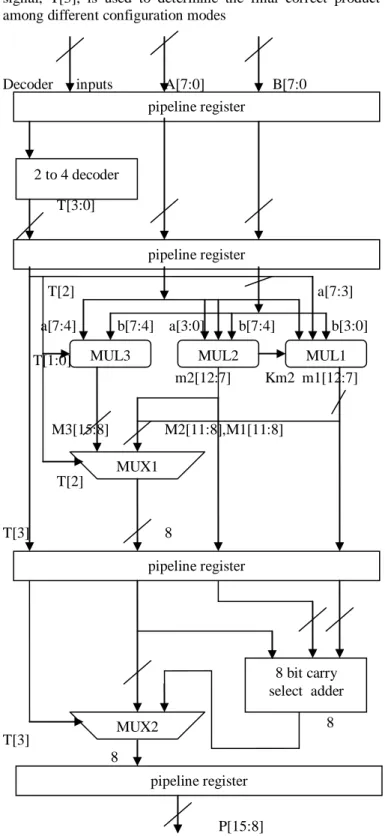
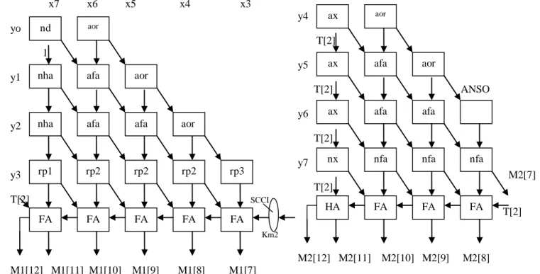
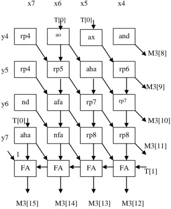
The 8 bit array based modified baugh-wooley multiplier with four stages of pipelined structure which is shown in fig 1.it consists of 2 to 4 decoder, two multiplexers(MUX),three multipliers (MUL1,MUL2,MUL3). The architecture of MUL1, MUL2, MUL3 are shown in fig. 2,fig. 4,fig. 6 respectively. The building blocks for MUL1, MUL2, MUL3 are further shown in fig. 2, fig. 4, fig. 6 respectively. And in this architectures I use some notations ND, A, HA, FA represents a NAND gate, an AND gate, a half adder and full adder, respectively.
In the block diagram from Fig. 1. All modules are controlled by 2 to 4 decoder controlling signals { T[0], T[1], T[2], T[3] }, for the next processing as summarized in Table 1. Based on the control signals, the three multiplication modules can be manipulated at the second stage. A MUX is used in the second stage to select the output of MUL3 or the concatenated output of MUL1 and MUL2 as shown in Fig. 1. To minimize the error, two sub calibration circuits, SCC1 and SCC2, are used, as shown in Fig. 3 and Fig. 5, respectively.
TABLE I. DECODER TRUTH TABLE
Configuration Modes Control Signals
OP [1:0] T[3] T[2] T[1] T[0]
00 M1 1 0 0 0
01 M2 0 1 0 0
10 M3 0 0 1 0
11 M4 0 0 0 1
The third stage is responsible for the accumulation of the output values of MUL1, MUL2, MUL3 and selecting the output of final product according to the four configuration modes. As shown in Fig. 1, ADD1 adds the output of MUL1 and MUL2. The output bits of ADD1 only include carryout and ignores the LSB due to the fixed-width output of the multiplier. The output of ADD1 and the output of the MUX from the second stage are added using ADD2. A control
signal, T[3], is used to determine the final correct product among different configuration modes
Decoder inputs A[7:0] B[7:0
T[3:0] T[2] a[7:3] a[7:4] b[7:4] a[3:0] b[7:4] b[3:0] T[1:0] m2[12:7] Km2 m1[12:7] M3[15:8] M2[11:8],M1[11:8] T[2] T[3] 8 8 T[3] 8 P[15:8]
Fig. 1 Pipelined modified baugh-wooley multiplier. pipeline register
pipeline register
pipeline register pipeline register 2 to 4 decoder
MUL3 MUL2 MUL1
8 bit carry select adder MUX1
x7 x6 x5 x4 x3 yo 1 y1 y2 y3 T[2] SCCI Km2 M1[12] M1[11] M1[10] M1[9] M1[8] M1[7]
Fig. 2. Architecture for MUL1
Fig. 3. Building blocks of MUL1
x3 x2 x1 x0 y4 T[2] y5 T[2] ANSO y6 T[2] y7 M2[7] T[2] T[2] M2[12] M2[11] M2[10] M2[9] M2[8]
Fig. 4. Architecture for MUL2
Fig. 5. Building blocks of MUL2
nd aor nha rp1 nha afa afa rp2 rp2 afa rp2 FA FA rp3 FA aor aor FA FA ax aor ax nx ax afa afa nfa nfa afa nfa FA HA FA aor FA
x7 x6 x5 x4 T[0] T[0] y4 M3[8] y5 M3[9] y6 T[0] M3[10] y7 M3[11] 1 T[1] M3[15] M3[14] M3[13] M3[12]
Fig. 6. Architecture for MUL3
Fig. 7. Building blocks of MUL3
III. PERFORMANCE EVALUATION FOR DIFFERENT FAMILIES OF FPGAS
The modular 8×8 fixed-width Baugh-Wooley multiplier design is coded in VERILOG and synthesized using high-end state-of-the-art Xilinx 7 series FPGAs. Kintex-7 (xc7k70t-fbg676) and Zynq-7000 (xc7z010-1clg400) devices are selected as the target architectures synthesized and performance evaluation of the multiplier. At the logic level, these FPGA families are all based on 6-input LUTs and fabricated in an advanced 28 nm CMOS technology.
Each block of the multiplier is verified through simulation using ISE 14.7 simulator. The RTL schematic of the multiplier is shown in Fig. 8. Tables II, III, IV and V summarize the FPGA implementation results of the multiplier using different families of devices.
TABLE.II. FPGA DEVICE UTILIZATION SUMMARY FPGA Resources Kintex-7 Artix-7
Used/Available Used/Available Slice LUTs 73/41000 59/63400 Delay (ns) 3.339 5.839 Max frequency(MHz) 299.49 171.36 Power consumption (mW) 80 82 TABLE.III
FPGA Resources Spartan=6 Zync-7000 Used/Available Used/Available Slice LUTs 59/2400 59/17600 Delay (ns) 10.777 4.489 Max frequency(MHz) 92.79 222.76 Power consumption (mW) 14 100 TABLE.IV
FPGA Resources Spartan-3a Sparatan-3E Used/Available Used/Available Slice LUTs 118/1408 67/970 Delay (ns) 15.054 14.685 Max frequency(MHz) 66.42 68.09 Power consumption (mW) 10 34 rp4 ao rp4 aha nd rp5 afa nfa rp8 rp7 rp8 FA FA FA aha rp7 FA ax and rp6
IV.CONCLUSIONS
In this paper mainly design and synthesized fixed width modified baugh-wooley multiplier using different families of FPGAs such as Kintex-7,zync-7000,Spartan-6,Spartan-3a and Spartan-3E. the design has been coded in VERIOG with Software platform of Xilinx ISE 14.7. from the synthesized results evaluated different characteristics of multiplier such as power, speed, area. As future extension instead of fixed point arithmetic using of floating point arithmetic which is better accurate results for mostly advanced digital signal processors (DSP) applications.
REFERENCES
[1] L.-D.Van and J.-H.Tu,―Power-efficient pipelined reconfigurable fixed-width baugh-wooley multipliers,‖ IEEE Trans. Computers, Vol. 58, No. 10, pp. 1346-1355, Oct. 2009.
[2] R. C. Baugh and A. B. Wooley, ―A two’s complement parallel array multiplication algorithm,‖ IEEE Trans. Computers, Vol. C-22, No. 12, 1045-1047, Dec. 1973.
[3] J. M. Jou, S. R. Kuang, and R. D. Chen, ―Design of low-error fixed-width multipliers for DSP applications,‖ IEEE Trans. Circuits Syst. II, Analog Digit. Signal Process., Vol. 46, No. 6, pp. 836-842, June 1999. [4] S. Gao, D. Al-Khalili and N. Chabini, ―Efficient realization of large size
two's complement multipliers using embedded blocks in FPGAs,‖ J. Circuits Syst. Signal Process., Vol. 27, No. 5, pp. 713-731, Oct. 2008. [5] T. -B. Juang and S. -F. Hsiao, ―Low-error carry-free fixed-width
multipliers with low-cost compensation circuits‖, IEEE Trans. Circuits Syst. II, Vol. 52, No. 6, pp. 209-303, June 2005.
[6] K. -J. Cho, K. -C. Lee, J. -G. Chung and K. K. Parhi, ―Design of low-error fixed-width modified booth multiplier,‖ IEEE Trans. Very Large Scale Integration (VLSI) Systems, Vol. 12, No. 5, pp. 522-531, May 2004.
[7] S. -M. Kim, J. -G. Chung and K. K. Parhi, ―Low error fixed-width CSD multiplier with efficient sign extension,‖ IEEE Trans. Circuits Syst. II, Vol. 50, No. 12, pp. 984-993, Dec. 2003
[8] http://www.xilinx.com/support/documentation/sw_manuals/xilinx14_7/ hh_goto.htm#ise_c_design_strategies.htm [Online, Accessed: 2 Feb, 2015]
[9] B. Parhami, Computer Arithmetic: Algorithms and Hardware Designs. Oxford, U.K.: Oxford Univ. Press, 2000, pp. 93–96
[10] E. J. King and E. E. Swartzlander, Jr., ―Data-dependent truncation scheme for parallel multipliers,‖ in Proc. 31st Asilomar Conf. Signals, Systems, and Computers, Pacific Grove, CA, 1997, pp. 1178–1182 [11] E. E. Swartzlander, Jr., ―Truncated multiplication with approximate
rounding,‖ in Proc. 31st Asilomar Conf. Signals, Systems, and Com- puters, Pacafic Grove, CA, 1999, pp. 1480–1483
[12] O.L. MacSorley, ―High-Speed Arithmetic in Binary Computer,‖ Proc. Conf. Institute of Radio Engineers (IRE ’61), vol. 49, pp. 67-91, 1961.
About authors:
1) K.Durgarao, M.tech student of Amrita sai institute of science and technology.
2) B.suresh, Assistant professor in the dept ECE, Amrita sai institute of science and technology, Paritala.
3) G.Sivakumar, Assistant professor in the dept ECE, Amrita sai institute of science and technology, Paritala.
4) M.Divaya manasa, Assistant professor in the dept ECE, Amrita sai institute of science and technology, Paritala.